Article

Water Vapor-Impermeable AlON/HfOx Bilayer Films Deposited by Hybrid High-Power Impulse Magnetron Sputtering/Radio-Frequency Magnetron Sputtering Processes

1
Department of Materials Engineering, Ming Chi University of Technology, New Taipei City 24301, Taiwan
2
Center for Plasma and Thin Film Technologies, Ming Chi University of Technology, New Taipei City 24301, Taiwan
*
Author to whom correspondence should be addressed.
Materials 2024, 17(22), 5453; https://doi.org/10.3390/ma17225453
Submission received: 10 October 2024 / Revised: 27 October 2024 / Accepted: 6 November 2024 / Published: 8 November 2024

Abstract

:
Water vapor-impermeable AlON/HfOx bilayer films were constructed through a hybrid high-power impulse magnetron sputtering (HiPIMS) and radio-frequency magnetron sputtering process (RFMS), applied as an encapsulation of flexible electronics such as organic photovoltaics. The deposition of monolithic and amorphous AlON films through HiPIMS was investigated by varying the duty cycles from 5% to 20%. At an accelerated test condition, 60 °C, and 90% relative humidity, a 100 nm thick monolithic AlON film prepared using a duty cycle of 20% exhibited a low water vapor transmission rate (WVTR) of 0.0903 g m−2 day−1 after testing for 336 h. Furthermore, after introducing a nanocrystalline HfOx film through RFMS, a 214 nm thick AlON/HfOx bilayer film reached the lowest WVTR of 0.0126 g m−2 day−1.

1. Introduction

Flexible electronic devices have received much attention due to their prospective applications in rollup displays and flexible smart mobile devices. Polymer substrates are essential in flexible electronic devices, such as organic photovoltaics, thin-film transistors, and light-emitting diodes [1]. However, the severe water vapor permeability of polymer materials manifestly restricts the lifetime of flexible electronic devices. The familiar plastic substrates include polyethylene terephthalate (PET), polyimide, and polycarbonate. An essential concern for flexible electronics is their degradation, as they are susceptible to environmental moisture and oxygen, resulting in a short lifetime [2]. Therefore, constructing a thin-film encapsulation (TFE) layer has become a key technology for realizing flexible polymer devices. Various inorganic compounds, such as SiOx [3,4], Al2O3 [5], AlOxNy [6], TiOx [7,8], and SiNx [9], or their mixed oxides (Al2O3/HfO2 [10]) have been investigated as TFE layers. The processes for fabricating TFE layers need to be controlled at low temperatures due to the use of plastic substrates [10,11]. A low defect density is favored for preventing gas permeation [3,10]. Moreover, transparency to light is crucial for optoelectronic devices [3,10,11]. Al2O3 thin films with dense and defect-free structures fabricated by atomic layer deposition (ALD) have been developed as gas permeation barriers for organic light-emitting diode (OLED) devices, which show a water vapor transmission rate (WVTR) of 1 × 10⁻³ g m−2 day−1 when the film thickness is 26 nm and deposited on polyethylene naphthalate (PEN) substrates [12]. However, restrictions on the deposition temperatures and low deposition rates were the weaknesses of conventional ALD processes. The glass transition temperature (Tg) of PEN is 126 °C. Though the ALD process performed in [12] was controlled at 120 °C, the deposition cycle was 60.25 s for the Al2O3 film, and the deposition rate was 0.12 nm/cycle. Moreover, plasma-assisted atomic layer deposition (ALD) has succeeded in developing moisture-impermeable Al2O3 barriers on PEN substrates using a low cycle of 17 s. It exhibits a WVTR of 5 × 10⁻³ g m−2 day−1 when the 20 nm thick film is deposited at room temperature [5]. Kim et al. [10] reported that 20 and 50 nm thick amorphous Al2O3 layers fabricated by plasma-enhanced ALD on PEN substrates had WVTRs of 2.92 × 10⁻³ and 3.26 × 10⁻⁴ g m−2 day−1, respectively, which increased by one order of magnitude when these films were grown at 100 °C. Similar increases in the WVTR with film thickness were obtained for the crystalline HfO2 and amorphous Al2O3/HfO2 mixed films. The 50 nm thick HfO2 film had a high WVTR of 6.75 × 10⁻² g m−2 day−1, which was ascribed to its crystalline structure and provided moisture permeation pathways along grain boundaries and voids. In contrast, the 50 nm thick Al2O3/HfO2 films had a low WVTR of 1.44 × 10⁻⁴ g m−2 day−1.
The specifications of WVTR differ from those of various applications. The WVTR is 1–10 g m−2 day−1 for food packaging, 0.01 g m−2 day−1 for flexible electronic devices, and 10−6 g m−2 day−1 for the OLEDs [13]. The TFE layers for OLEDs with low moisture permeation are obtained through the ALD technique or inorganic and organic multilayer formations [14]. PET has been applied for versatile purposes, such as food storage, with a TFE layer for flexible device packaging [11]. Ascribing to the low Tg temperature of 66 °C for the amorphous PET, the utility of the expansive ALD process for raising moisture impermeability for PET is not worth developing. High-power impulse magnetron sputtering (HiPIMS) reveals the principal characteristics of the high ionization of the sputtered material [15], which resulted in the formation of densified films well adhered to the substrate and a droplet-free surface. HiPIMS technology is exemplified by low duty cycles, repetition frequency, and high power densities [16]. In this study, we prepared AlON films on PET substrates at room temperature through HiPIMS to improve the impermeability against water vapor and sustain high transparency. Moreover, HfOx films were reported to have high chemical stability [10]. Radio-frequency magnetron sputtering (RFMS) was widely applied to coat the oxide layers. A hybrid HiPIMS/RFMS was employed to advance the films’ quality and deposition rates [17]. Therefore, combining the benefits of AlON and HfOx films is a crucial attempt to develop TFE candidates. In this study, AlON/HfOx bilayer films were fabricated by hybrid HiPIMS/RFMS. The water vapor transmission rates (WVTRs) of the AlON/HfOx bilayer films were evaluated.

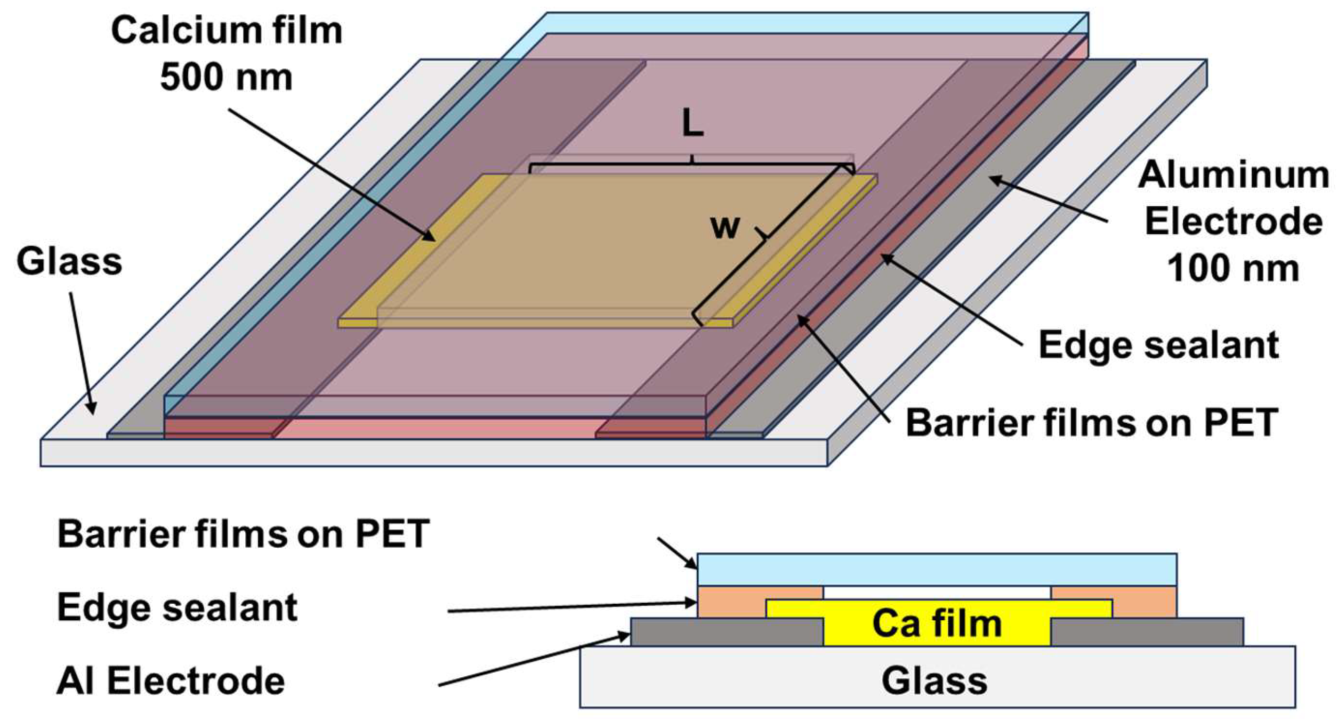
2. Materials and Methods

The monolithic AlON and HfOx films with a thickness of 97–110 nm and AlON/HfOx and HfOx/AlON bilayer films with a thickness of approximately 200 nm were fabricated on 50 μm thick PET sheets (BH216, Nan Ya Plastics, Taipei, Taiwan), glass slides (76 mm × 25 mm × 1 mm), and Si wafers. The substrate temperature was set at room temperature and heated by plasma to 43 °C during deposition, which did not exceed the Tg of 66 °C for the amorphous PET. The monolithic AlON films were prepared through HiPIMS using an Al target of 76.2 mm in diameter under an average power of 300 W. The samples D5, D10, D15, and D20 were prepared using on/off times of 50/950, 100/900, 150/850, and 200/800 μs in an HiPIMS cycle, respectively, representing a duty cycle of 5%, 10%, 15%, and 20% and a peak power density of 816, 481, 347, and 259 W/cm2, respectively. The introduced gas comprised 15 sccm Ar, 12 sccm N2, and 3 sccm O2, and the working pressure was maintained at 29 mPa. After depositing for 165 min, the thicknesses of samples D5, D10, D15, and D20 were 99, 97, 102, and 108 nm, respectively. The monolithic HfOx films were prepared using an HfO2 target of 76.2 mm diameter in the chamber purged with 30 sccm Ar. The thickness of HfOx films was 110 nm after depositing for 30 min. The AlON/HfOx and HfOx/AlON bilayer films with various thickness ratios were laminated with monolithic D20 and HfOx films by varying the deposition times.
The monolithic AlON and HfOx films’ chemical compositions were analyzed using a field-emission electron probe microanalyzer (FE-EPMA, JXA-iHP200F, JEOL, Tokyo, Japan) equipped with wavelength dispersive spectrometers at a 3 kV accelerating voltage. No signals from Si substrates were detectable. Al2O3, KAl3O8, BN, and Hf were the standard samples for evaluating the Al, O, N, and Hf compositions, respectively. The films’ phases were verified using X-ray diffraction (XRD; X’Pert PRO MPD, PANalytical, Almelo, The Netherlands) with Cu Kα radiation using a grazing incidence technique at an incidence angle of 1°. Film thicknesses were examined using a field-emission scanning electron microscope (FE-SEM, JSM-IT700HR, JEOL, Tokyo, Japan). The surface roughness values of the films were evaluated using atomic force microscopy (Dimension 3100 SPM, NanoScope IIIa, Veeco, NY, USA). Ra and Rq signify the average and root-mean-square surface roughness, respectively. The average values and standard deviations of surface roughness and chemical composition were determined from three measurements. The nanostructures of the films were observed using transmission electron microscopy (TEM, JEM-2010E, JEOL, Akishima, Japan). The TEM samples with a protective C or Pt layer were prepared using a focused ion beam system (NX2000, Hitachi, Tokyo, Japan). Optical transmission was examined using a spectrophotometer (v-650, Jasco, Tokyo, Japan).
The WVTRs of AlON films were tested using a water vapor permeation analyzer (Aquatran Model 2, MOCON, Brooklyn Park, MN, USA) conducted at 60 °C in 90% relative humidity for 24 h. The MOCON instrument and calcium test are commonly used to determine films’ WVTR [9,18]. Moreover, a homemade calcium test system evaluated the WVTRs of AlON films and AlON/HfOx bilayer films at 60 °C in 90% relative humidity for 336 h. Figure 1 displays the sample structure for the calcium test in this study. The WVTR is determined as follows [10,18,19]:
W V T R = n δ C a ρ C a L e f f w A C a A B M H 2 O M C a d 1 / R d t ,
where n is the reaction ratio between water and Ca (2), δCa is the density of Ca (1.55 g/cm3), ρCa is the resistivity of Ca film (3.9 μΩcm), Leff (1 cm) and w (0.5 cm) are, respectively, the effective length and width of the Ca test lines, ACa/AB is the ratio of the Ca test sensor area to the H2O vapor barrier area (1), MH2O/MCa is the molecular weight ratio of H2O to Ca (18/40), d(1/R)/dt is the variation in conductivity with time t, and R is the resistivity. Three measurements were made to determine the WVTR values.

3. Results and Discussion

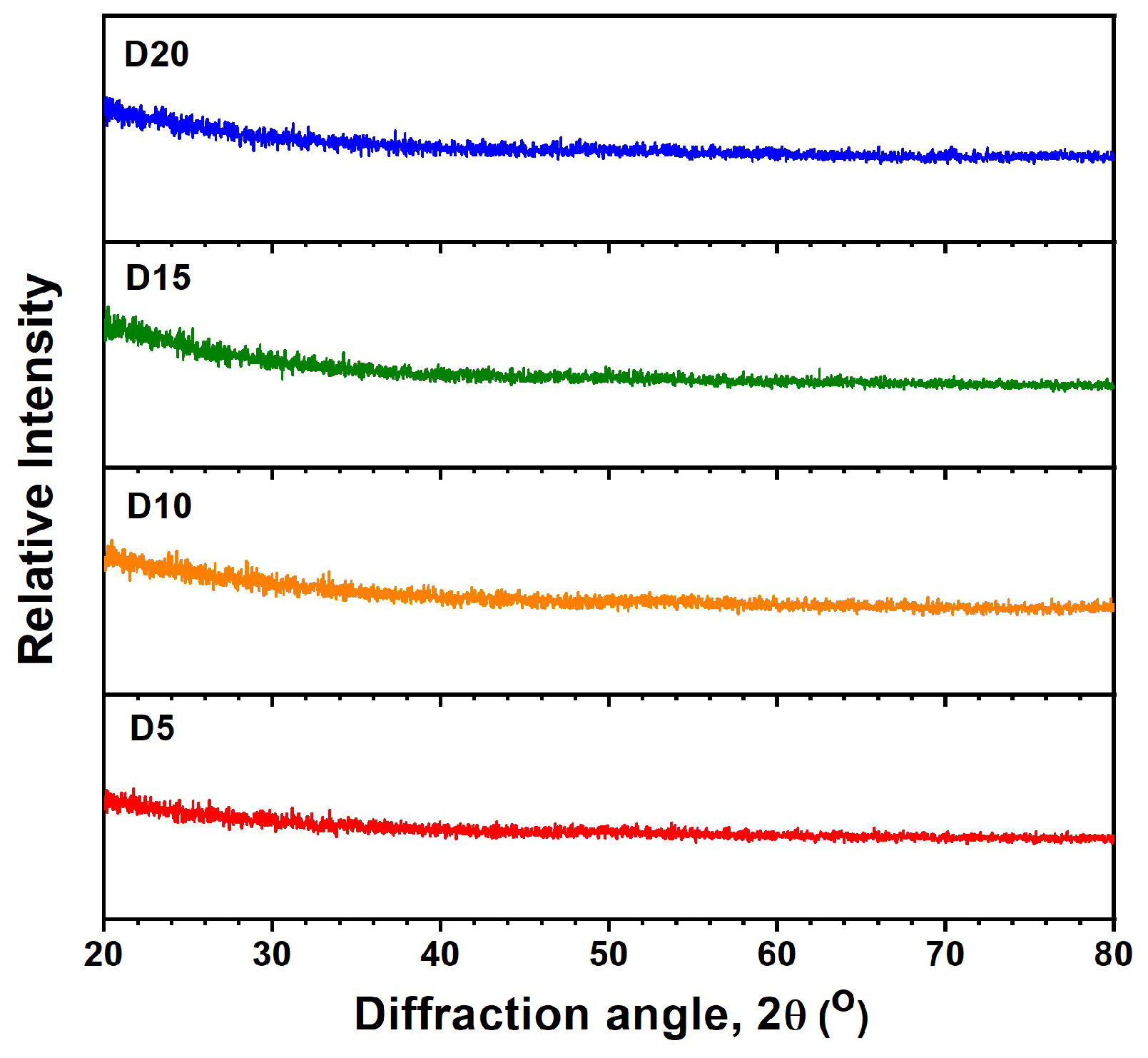
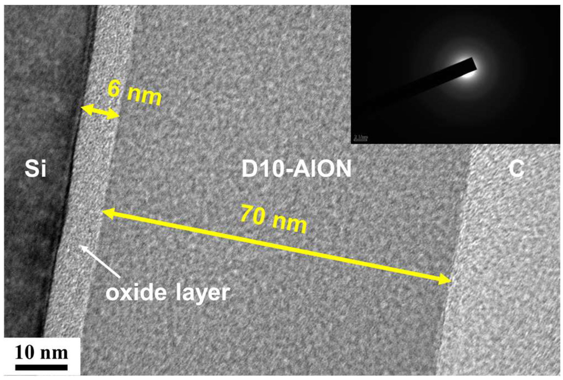
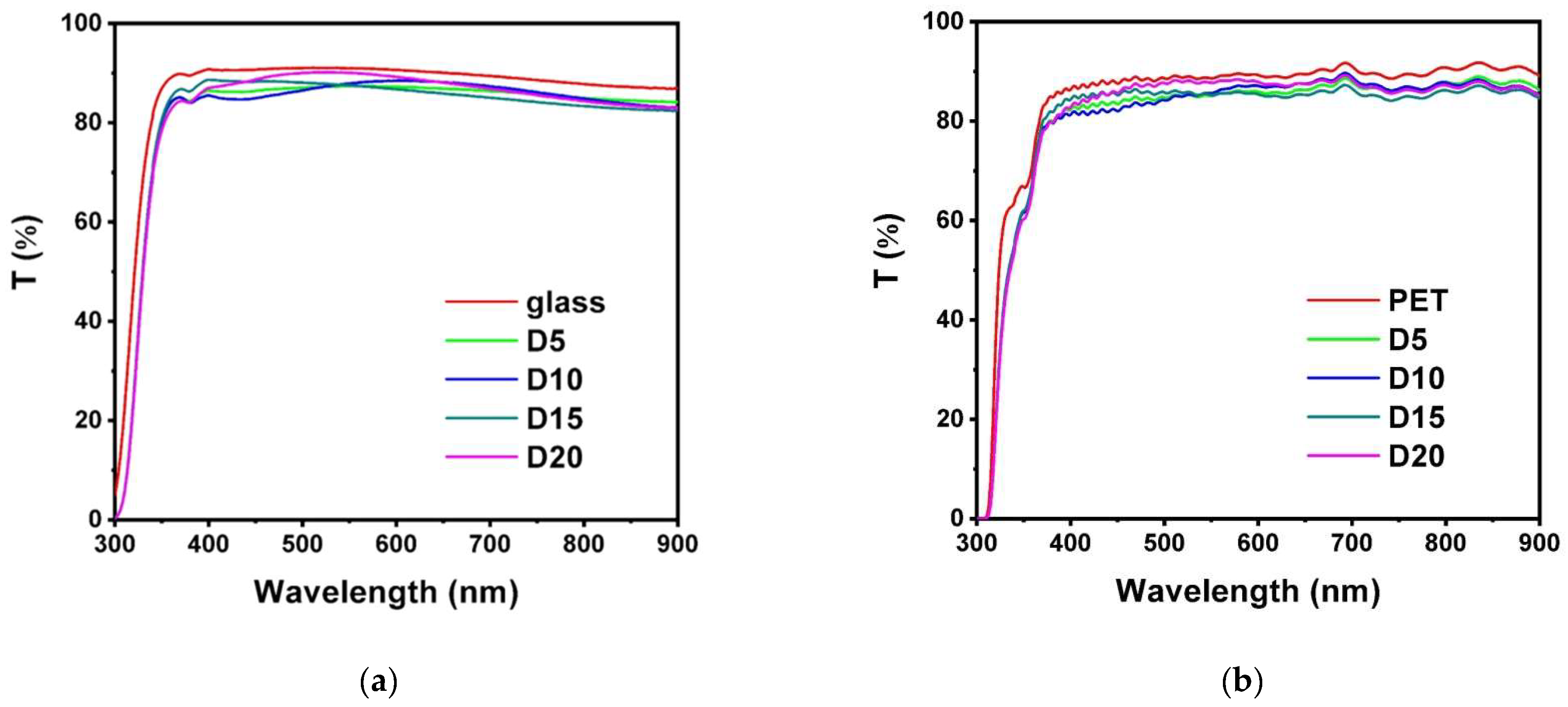
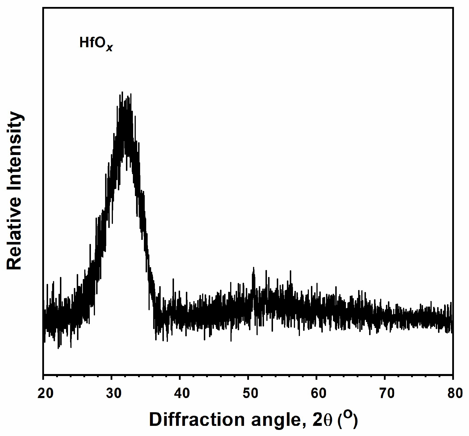
3.1. Monolithic AlON and HfOx Films

Table 1 shows the atomic compositions of the monolithic AlON films prepared by HiPIMS processes. The AlON films prepared using a duty cycle of 5% exhibited an atomic composition of 38.54% Al–59.31% O–2.15% N. The sputter gas flow consisted of 15 sccm Ar, 12 sccm N2, and 3 sccm O2. O and Al’s affinity was higher than N and Al’s. Moreover, the AlON films prepared using higher duty cycles of 10%, 15%, and 20% exhibited slightly higher O and lower Al and N contents. The stoichiometric ratios of anions to cations in Al2O3 and AlN compounds were 1.5 and 1, respectively. The required Al content to achieve stoichiometric Al2O3 and AlN, labeled as Al*, was higher than the realistic Al content. The Al*/Al ratios were 1.08, 1.14, 1.13, and 1.16 for D5, D10, D15, and D20 films, respectively, which implies that all of the fabricated monolithic AlON films were over-stoichiometric with extra O and N contents.
Figure 2 depicts the XRD patterns of the monolithic AlON films. All of the AlON films exhibited amorphous structures. Figure 3 displays a cross-sectional TEM image of the D10-AlON film prepared on a Si substrate. An oxide layer that was 6 nm thick formed on the Si substrate, and the D10 film exhibited an amorphous structure. The oxide layer consisted of native oxide and followed the diffusion of Si and O in the subsequent AlON deposition process. The selective area electron diffusion (SAED) pattern without clear spots or rings confirms the amorphous phase formation. Figure 4 shows the Ra and Rq values of the monolithic AlON films, which decreased from 0.50 to 0.06 nm and 0.60 to 0.08 nm, with duty cycles increasing from 5% to 20%. All of the Ra and Rq values were less than 0.6 nm, which was attributed to the formation of amorphous structures. Figure 5 exhibits the optical transmittance of the AlON films prepared on glass and PET substrates, respectively. The transmittance ratios at 530 nm of the glass substrate and the D5, D10, D15, and D20 films prepared on glass substrates were 91.0%, 87.3%, 87.5%, 87.8%, and 90.2%, respectively. In contrast, the transmittance ratios of the PET substrate and the D5, D10, D15, and D20 films prepared on PET substrates were 88.8%, 85.1%, 85.3%, 85.7%, and 87.9%, respectively. The transmittance ratios for the samples prepared on PET substrates were lower than those prepared on glass substrates, which were attributed to the difference between the transmittance ratios of the substrates. All of the roughness values of the films deposited on glass and PET substrates were <0.6 nm. The wavelength of visible light is far larger than the roughness of the samples; therefore, the influence of roughness on optical transmission can be negligible.
Figure 6 displays the WVTRs of the monolithic AlON films prepared on PET substrates. The WVTR analyzed using the water vapor permeation analyzer exhibited a decreasing trend from 0.3040 to 0.1802, 0.1088, and 0.0972 g m−2 day−1 when the duty cycle for fabricating AlON films increased from 5% to 10%, 15%, and 20%. The WVTR evaluated by the calcium test decreased from 0.2933 to 0.1768, 0.1113, and 0.0903 g m−2 day−1 when the duty cycle increased from 5% to 10%, 15%, and 20%, which exhibited a highly consistent trend relative to that examined by the water vapor permeation analyzer. The increase in the duty cycle of the HiPIMS process resulted in a decrease in the impact energy of the sputtered atoms and decreased defect formation, which reduced the diffusion paths of the moisture and the WVTR.
The atomic composition of the monolithic HfOx films prepared through RFMS was 40.53 ± 0.18% Hf and 59.47 ± 0.18% O. The stoichiometric ratio of O/Hf was 1.47 (<2), which implied that the monolithic HfOx films were under-stoichiometric. Figure 7 depicts the XRD pattern of the monolithic HfOx films, revealing a nanocrystalline structure with a broad reflection at around a 2θ angle of 32°.

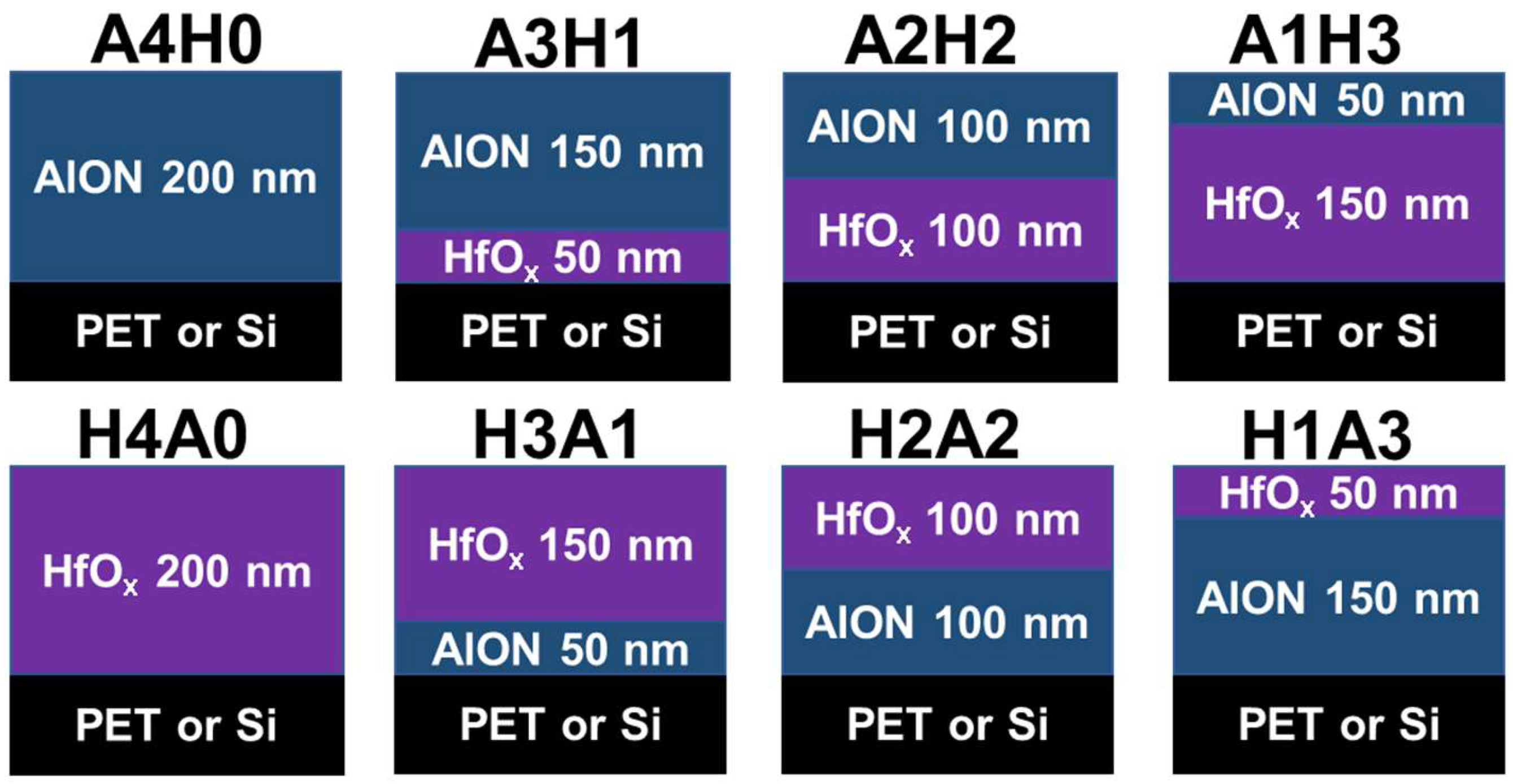
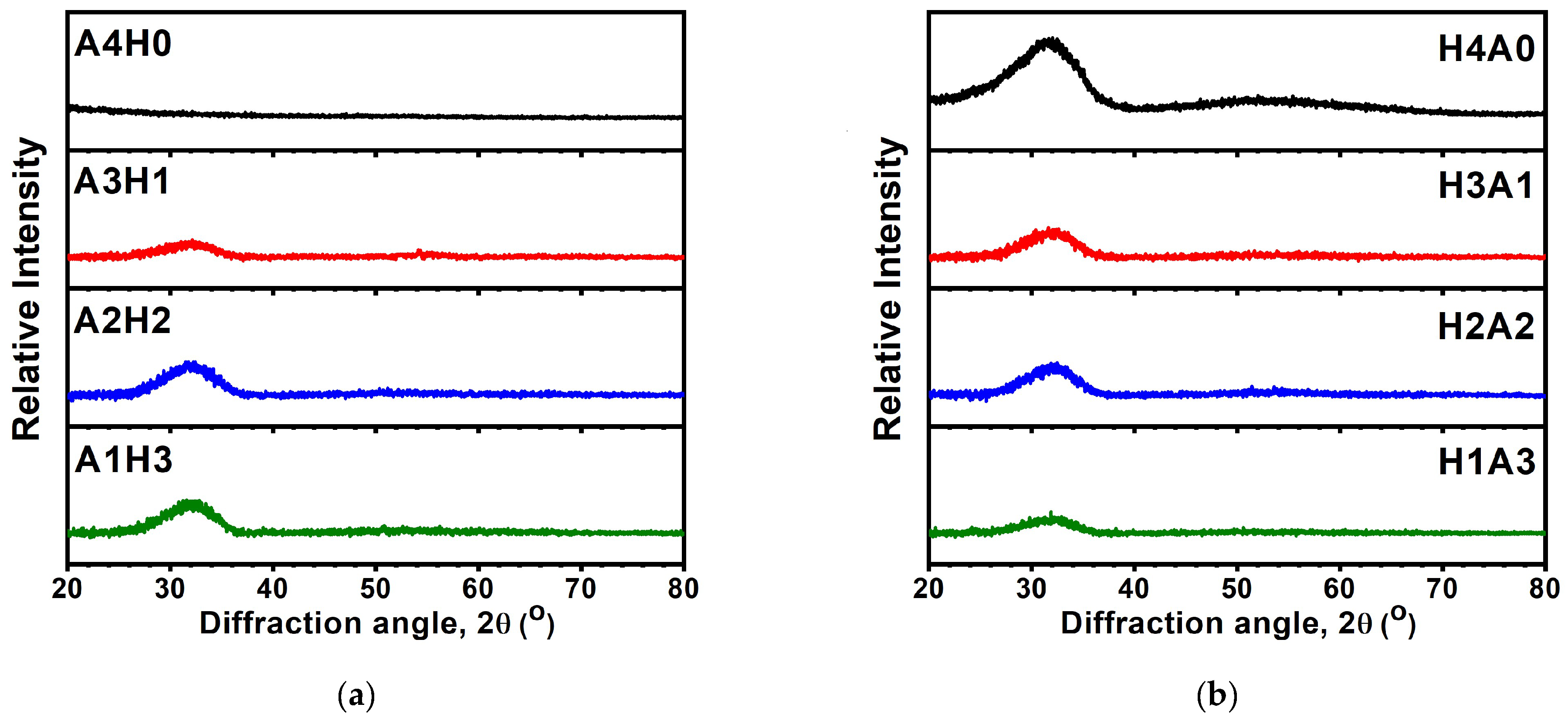
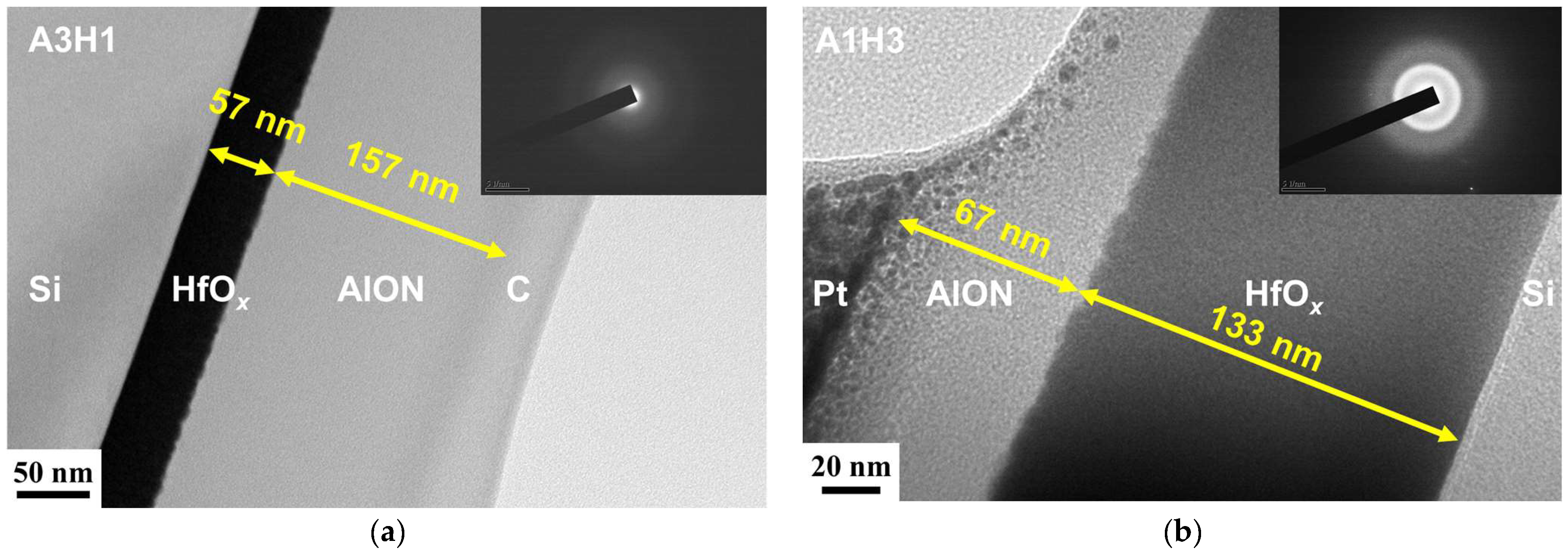
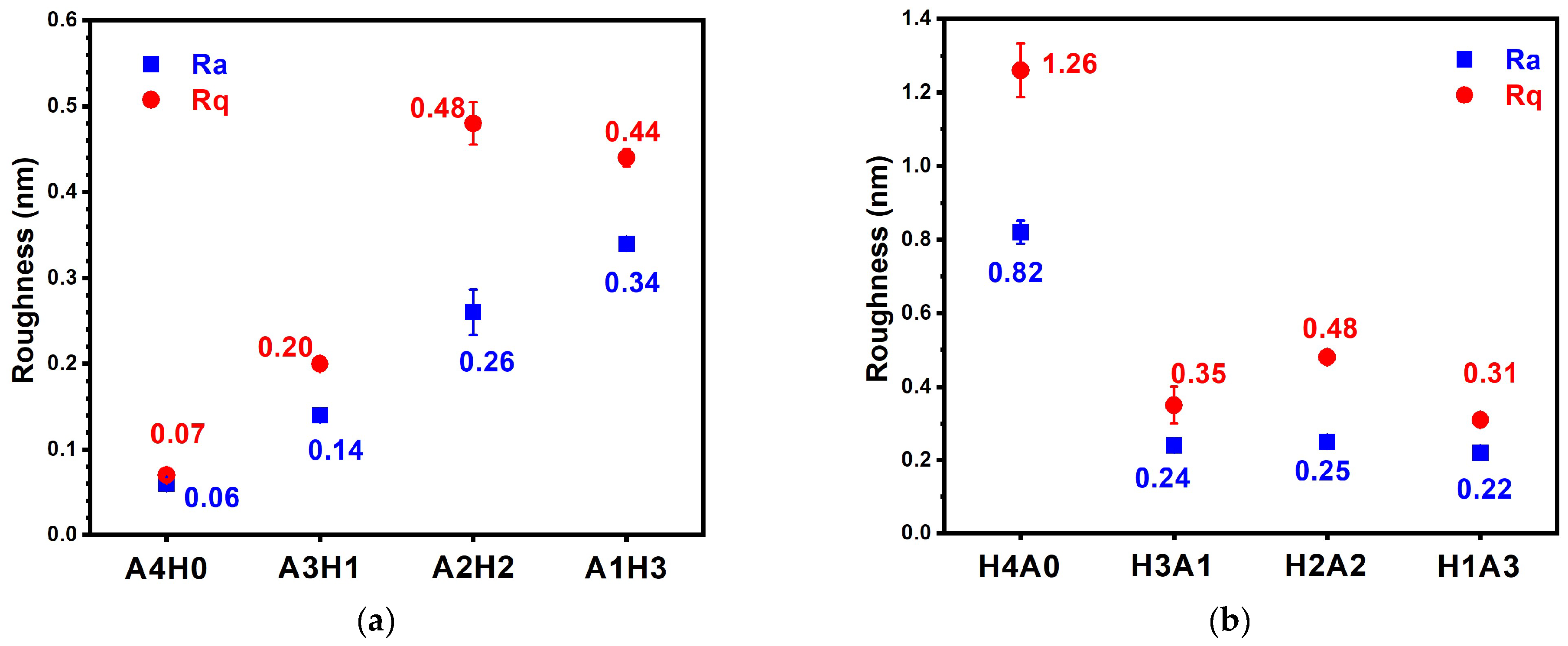
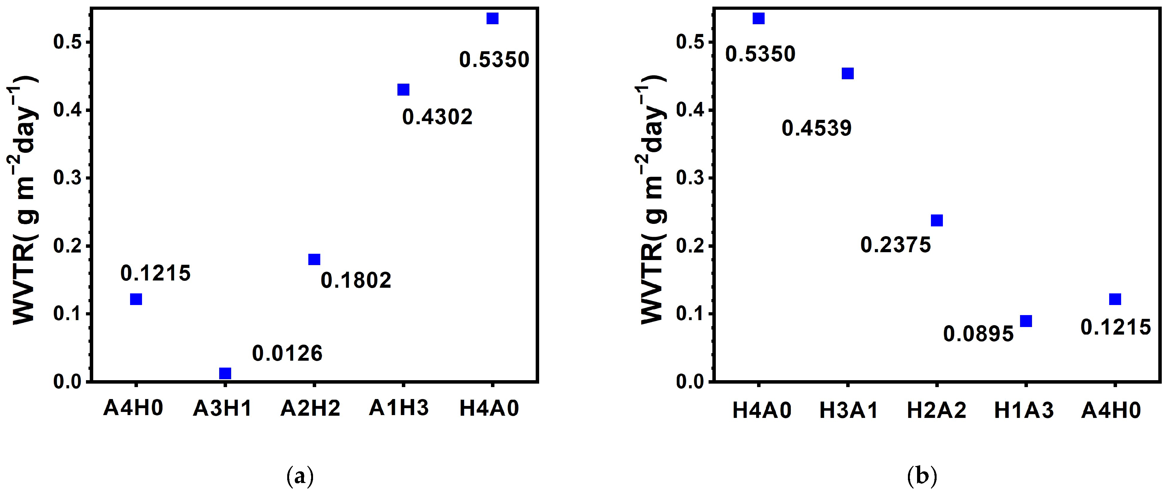
3.2. AlON/HfOx Bilayer Films

Figure 8 displays the design of the AlON/HfOx and HfOx/AlON bilayer films. The monolithic AlON and HfOx films with a higher thickness of approximately 200 nm were also prepared for comparison and renamed A4H0 and H4A0, respectively. According to the deposition rates of the monolithic D20 and HfOx samples, the bilayer films were regulated by various deposition times. For example, the A3H1 bilayer films were deposited using the condition for fabricating HfOx for 10 min and then deposited using the condition for preparing AlON(D20) for 120 min. The A2H2 bilayer films were deposited on an HfOx sublayer for 20 min and an AlON(D20) sublayer for 80 min. The A1H3 bilayer films were deposited on an HfOx sublayer for 30 min and an AlON(D20) sublayer for 40 min. Figure 9 displays the XRD patterns of the AlON/HfOx and HfOx/AlON bilayer films. The A4H0 film, a thicker monolithic D20 film, exhibited amorphous structures. In contrast, the A3H1, A2H2, and A1H3 AlON/HfOx bilayer films revealed nanocrystalline structures, ascribed to the HfOx sublayers. Figure 10 depicts cross-sectional TEM images of the A3H1 and A1H3 films. The A3H1 film is stacked with a 57 nm thick HfOx sublayer and a 157 nm thick AlON sublayer. The SAED pattern correlated to the AlON sublayer exhibits amorphous structures. The A1H3 film is stacked with a 133 nm thick HfOx sublayer and a 67 nm thick AlON sublayer. The SAED pattern correlated to the HfOx sublayer reveals a nanocrystalline structure.
Figure 11 shows the surface roughness values of the AlON/HfOx and HfOx/AlON bilayer films. All of the bilayer films exhibited Ra and Rq values of less than 0.5 nm. The monolithic A4H0 films exhibited Ra and Rq values of <0.1 nm, which was attributed to the amorphous structure, as observed from the XRD pattern of the A4H0 film and the SAED pattern of the A3H1 film. Combined with amorphous AlON sublayers, the AlON/HfOx and HfOx/AlON bilayer films revealed low surface roughness values. In contrast, the monolithic H4A0 film exhibited high Ra and Rq values of 0.82 and 1.26 nm, respectively. The low surface roughness values of the bilayer films were dominated by the presence of an AlON sublayer either in the top or bottom layers.
Figure 12 exhibits the WVTRs of the AlON/HfOx and HfOx/AlON bilayer films examined by the calcium test at 60 °C in 90% RH for 336 h. The monolithic A4H0 film with a designed thickness of 200 nm showed a WVTR of 0.1215 g m−2 day−1, which was slightly higher than the 0.0903 g m−2 day−1 of the D20-AlON film with a thickness of 108 nm. Chen et al. [11] reported chemical vapor-deposited diamond-like carbon films with a thickness of 793 nm on PET substrates (47 μm thick), revealing a WVRT of 0.12 g m−2 day−1 at 25 °C in 80% RH. Lee et al. [20] reported plasma-enhanced chemical vapor-deposited SiNx and SiOx films (200 nm thick) on PET (100 μm thick), exhibiting WVRTs of 0.03 and 0.06 g m−2 day−1 at 60 °C in 90% RH after 10 days of testing. The A3H1 bilayer film has the thickest AlON top sublayer and exhibits the lowest WVTR among the AlON/HfOx bilayer films at 0.0126 g m−2 day−1. With the decreasing thickness of the AlON top layer, the A2H2 bilayer film exhibits a higher WVTR of 01802 g m−2 day−1. Moreover, the A1H3 bilayer film with a successively decreased AlON thickness has a much higher WVTR of 0.4302 g m−2 day−1. However, this is lower than 0.5350 g m−2 day−1 for the monolithic H4A0 film. The WVTR of the H4A0 film is 4.4 times greater than that of the A4H0 film. The bilayer film with a higher AlON thickness ratio exhibits a lower WVTR. In contrast, the A3H1 film has a WVTR lower than 0.1215 g m−2 day−1 of the A4H0 film, ascribed to the chemically stable HfOx sublayer [10]. Moreover, the formation of a hetero-interface between the AlON and HfOx sublayers could play a vital role in restricting moisture permeation. The effect of the heterointerface will be investigated in a future study by evaluating the WVTRs of multilayers with various stacking periods. On the other hand, the HfOx/AlON bilayer films exhibited a similar trend in WVTR with the AlON sublayer’s thickness variation.

4. Conclusions

Monolithic AlON film and AlON/HfOx and HfOx/AlON bilayer films were fabricated through hybrid HiPIMS/RFMS processes to evaluate their applications as water vapor-impermeable films on PET. The AlON and HfOx films were amorphous and nanocrystalline, respectively. The WVTR evaluated using a calcium test system revealed highly reliable results that agreed with those examined by the water vapor permeation analyzer. The AlON films exhibited a lower WVTR than that of the HfOx films. Moreover, the AlON/HfOx and HfOx/AlON bilayer films with higher thickness ratios of AlON/HfOx have lower WVTRs than the monolithic AlON films. The lowest WVTR of 0.0126 g m−2 day−1 was obtained for 214 nm thick AlON/HfOx bilayer films after testing at 60 °C under 90% relative humidity for 336 h.

Author Contributions

Conceptualization, L.-C.C.; validation, L.-C.C.; formal analysis, S.-E.L.; investigation, S.-E.L.; resources, L.-C.C.; writing—original draft preparation, L.-C.C.; project administration, L.-C.C.; funding acquisition, L.-C.C. All authors have read and agreed to the published version of the manuscript.

Funding

The National Science and Technology Council, Taiwan, funded this research with grant numbers 112-2221-E-131-011 and 113-2224-E-131-001. Ming Chi University of Technology funded the APC.

Institutional Review Board Statement

Not applicable.

Informed Consent Statement

Not applicable.

Data Availability Statement

Data are contained within the article.

Acknowledgments

The support for the FIB analysis from the Joint Center for High Valued Instruments at NSYSU is acknowledged.

Conflicts of Interest

The authors declare no conflicts of interest. The funders had no role in the study’s design, in the collection, analyses, or interpretation of data, in the writing of the manuscript, or in the decision to publish the results.

References

  1. Nathan, A.; Ahnood, A.; Cole, M.T.; Lee, S.; Suzuki, Y.; Hiralal, P.; Bonaccorso, F.; Hasan, T.; Garcia-Gancedo, L.; Dyadyusha, A.; et al. Flexible electronics: The next ubiquitous platform. Proc. IEEE 2012, 100, 1486–1517. [Google Scholar] [CrossRef]
  2. Yu, D.; Yang, Y.Q.; Chen, Z.; Tao, Y.; Liu, Y.F. Recent progress on thin-film encapsulation technologies for organic electronic devices. Opt. Commun. 2016, 362, 43–49. [Google Scholar] [CrossRef]
  3. Yanaka, M.; Henry, B.M.; Roberts, A.P.; Grovenor, C.R.M.; Briggs, G.A.D.; Sutton, A.P.; Miyamoto, T.; Tsukahara, Y.; Takeda, N.; Chater, R.J. How cracks in SiOx-coated polyester films affect gas permeation. Thin Solid Films 2001, 397, 176–185. [Google Scholar] [CrossRef]
  4. Roberts, A.P.; Henry, B.M.; Sutton, A.P.; Grovenor, C.R.M.; Briggs, G.A.D.; Miyamoto, T.; Kano, M.; Tsukahara, Y.; Yanaka, M. Gas permeation in silicon-oxide/polymer (SiOx/PET) barrier films: Role of the oxide lattice, nano-defects and macro-defects. J. Memb. Sci. 2002, 208, 75–88. [Google Scholar] [CrossRef]
  5. Langereis, E.; Creatore, M.; Heil, S.B.S.; van de Sanden, M.C.M.; Kessels, W.M.M. Plasma-assisted atomic layer deposition of Al2O3 moisture permeation barriers on polymers. Appl. Phys. Lett. 2006, 89, 081915. [Google Scholar] [CrossRef]
  6. Erlat, A.G.; Henry, B.M.; Grovenor, C.R.M.; Briggs, A.G.D.; Chater, R.J.; Tsukahara, Y. Mechanism of water vapor transport through PET/AlOxNy gas barrier films. J. Phys. Chem. B 2004, 108, 883–890. [Google Scholar] [CrossRef]
  7. Park, S.; Kim, L.H.; Jeong, Y.J.; Kim, K.; Park, M.; Baek, Y.; An, T.K.; Nam, S.; Jang, J.; Park, C.E. Reduced water vapor transmission rates of low-temperature processed and sol-gel-derived titanium oxide thin films on flexible substrates. Org. Electron. 2016, 36, 133–139. [Google Scholar] [CrossRef]
  8. Cho, S.; Lee, K.; Heeger, A.J. Extended lifetime of organic field-effect transistors encapsulated with titanium sub-oxide as an “active” passivation/barrier layer. Adv. Mater. 2009, 21, 1941–1944. [Google Scholar] [CrossRef]
  9. Yun, S.J.; Abidov, A.; Kim, S.; Choi, J.S.; Cho, B.S.; Chung, S.C. Water vapor transmission rate property of SiNx thin films prepared by low temperature (<100 °C) linear plasma enhanced chemical vapor deposition. Vacuum 2018, 48, 33–40. [Google Scholar]
  10. Kim, L.H.; Jang, J.H.; Jeong, Y.J.; Kim, K.; Baek, Y.; Kwon, H.J.; An, T.K.; Nam, S.; Kim, S.H.; Jang, J.; et al. Highly-impermeable Al2O3/HfO2 moisture barrier films grown by low-temperature plasma-enhanced atomic layer deposition. Org. Electron. 2017, 50, 296–303. [Google Scholar] [CrossRef]
  11. Chen, R.; Le, K.; Liu, Y.; Zheng, X.; Zhu, X.; Bao, L.; Yang, Z.; Xu, S.; Liu, W. Investigation of water vapor barrier performances of diamond-like carbon coatings on flexible PET fabricated at room temperature. Surf. Coat. Technol. 2024, 477, 130339. [Google Scholar] [CrossRef]
  12. Groner, M.D.; George, S.M.; McLean, R.S.; Carcia, P.F. Gas diffusion barriers on polymers using Al2O3 atomic layer deposition. Appl. Phys. Lett. 2006, 88, 051907. [Google Scholar] [CrossRef]
  13. Han, Y.C.; Jang, C.; Kim, K.J.; Choi, K.C.; Jung, K.H.; Bae, B.S. The encapsulation of an organic light-emitting diode using organic–inorganic hybrid materials and MgO. Org. Electron. 2011, 12, 609–613. [Google Scholar] [CrossRef]
  14. Bang, S.H.; Hwang, N.M.; Kim, H.L. Permeation barrier properties of silicon oxide films deposited on polyethylene terephthalate (PET) substrate using roll-to-roll reactive magnetron sputtering system. Microelectron. Eng. 2024, 166, 39–44. [Google Scholar] [CrossRef]
  15. Ehiasarian, A.P. High-power impulse magnetron sputtering and its applications. Pure Appl. Chem. 2010, 82, 1247–1258. [Google Scholar] [CrossRef]
  16. Sarakinos, K.; Alami, J.; Konstantinidis, S. High power pulsed magnetron sputtering: A review on scientific and engineering state of the art. Surf. Coat. Technol. 2010, 204, 1661–1684. [Google Scholar] [CrossRef]
  17. Chang, L.C.; Wu, C.E.; Ou, T.Y. Mechanical properties and diffusion barrier performance of CrWN coatings fabricated through hybrid HiPIMS/RFMS. Coatings 2021, 11, 690. [Google Scholar] [CrossRef]
  18. Jarvis, K.L.; Evans, P.J.; Cooling, N.A.; Vaughan, B.; Habsuda, J.; Belcher, W.J.; Bilen, C.; Griffiths, G.; Dastoor, P.C.; Triani, G. Comparing three techniques to determine the water vapour transmission rates of polymers and barrier films. Surf. Interfaces 2017, 9, 182–188. [Google Scholar] [CrossRef]
  19. Kempe, M.D.; Reese, M.O.; Dameron, A.A. Evaluation of the sensitivity limits of water vapor transmission rate measurements using electrical calcium test. Rev. Sci. Instrum. 2013, 84, 025109. [Google Scholar] [CrossRef] [PubMed]
  20. Lee, W.J.; Cho, T.Y.; Choa, S.H.; Cho, S.K. Environmental reliability and moisture barrier properties of silicon nitride and silicon oxide films using roll-to-roll plasma enhanced chemical vapor deposition. Thin Solid Films 2021, 720, 138524. [Google Scholar] [CrossRef]
Figure 1. Structure of the calcium test for WVTR measurement.
Materials 17 05453 g001
Figure 2. XRD patterns of monolithic AlON films prepared using various duty cycles in HiPIMS processes.
Materials 17 05453 g002
Figure 3. Cross-sectional TEM image of the D10-AlON film.
Materials 17 05453 g003
Figure 4. Surface roughness values of monolithic AlON films prepared on Si substrate.
Materials 17 05453 g004
Figure 5. Transmission of monolithic AlON films prepared on (a) glass and (b) PET.
Materials 17 05453 g005
Figure 6. WVTRs of the monolithic AlON films prepared on PET substrates and examined by a water vapor permeation analyzer for 24 h and calcium test for 336 h at 60 °C in 90% relative humidity.
Materials 17 05453 g006
Figure 7. XRD patterns of monolithic HfOx films.
Materials 17 05453 g007
Figure 8. Schemes of the bilayer films.
Materials 17 05453 g008
Figure 9. XRD patterns of (a) A4H0, A3H1, A2H2, and A1H3 and (b) H4A0, H3A1, H2A2, and H1A3 bilayer films.
Materials 17 05453 g009
Figure 10. Cross-sectional TEM and SAED patterns of (a) A3H1 and (b) A1H3 bilayer films.
Materials 17 05453 g010
Figure 11. Surface roughness values of (a) A4H0, A3H1, A2H2, and A1H3 and (b) H4A0, H3A1, H2A2, and H1A3 bilayer films.
Materials 17 05453 g011
Figure 12. WVTRs of (a) A4H0, A3H1, A2H2, and A1H3 AlON/HfOx bilayer films and (b) H4A0, H3A1, H2A2, and H1A3 HfOx/AlON bilayer films after testing at 60 °C in 90% RH for 336 h.
Materials 17 05453 g012
Table 1. Atomic compositions of AlON films.
SampleDuty CycleAtomic Compositions (at.%)
AlON
D55%38.54 ± 0.3359.31 ± 0.302.15 ± 0.25
D1010%37.13 ± 0.5561.10 ± 0.541.77 ± 0.15
D1515%37.51 ± 0.2760.61 ± 0.271.88 ± 0.12
D2020%36.89 ± 0.4161.26 ± 0.331.85 ± 0.20
Disclaimer/Publisher’s Note: The statements, opinions and data contained in all publications are solely those of the individual author(s) and contributor(s) and not of MDPI and/or the editor(s). MDPI and/or the editor(s) disclaim responsibility for any injury to people or property resulting from any ideas, methods, instructions or products referred to in the content.

