
In Situ Multiphysical Metrology for Photonic Wire Bonding by Two-Photon Polymerization

 ,
, 
Abstract
1. Introduction
2. Materials and Methods
2.1. Materials
2.2. PWB Fabrication and Characterization
2.3. FEM Simulation
3. Results and Discussion
3.1. In Situ Multiphysical Metrology
3.2. Laser Parameters of PWB by TPP
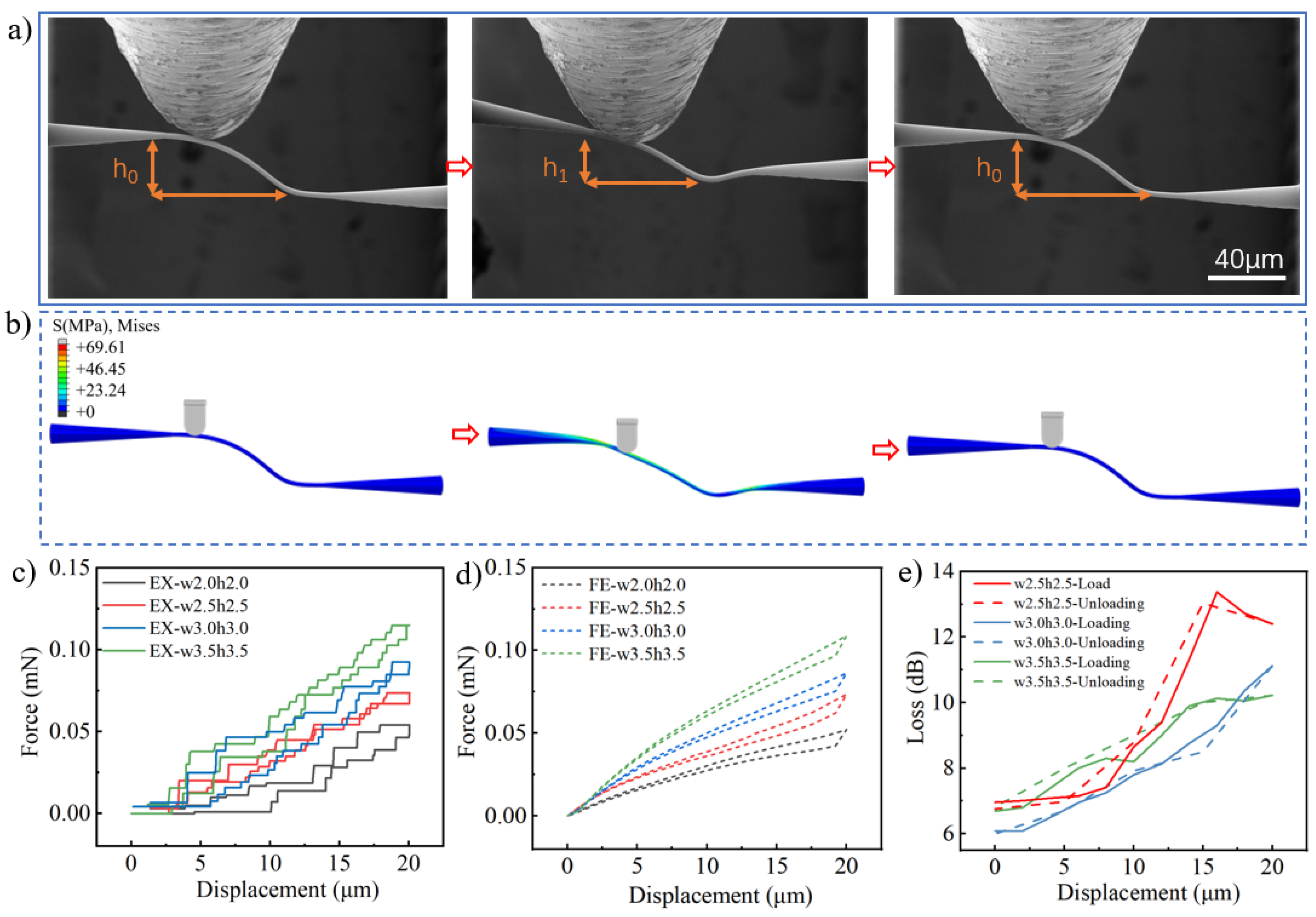
3.3. Geometrical Design for Low-Loss PWB
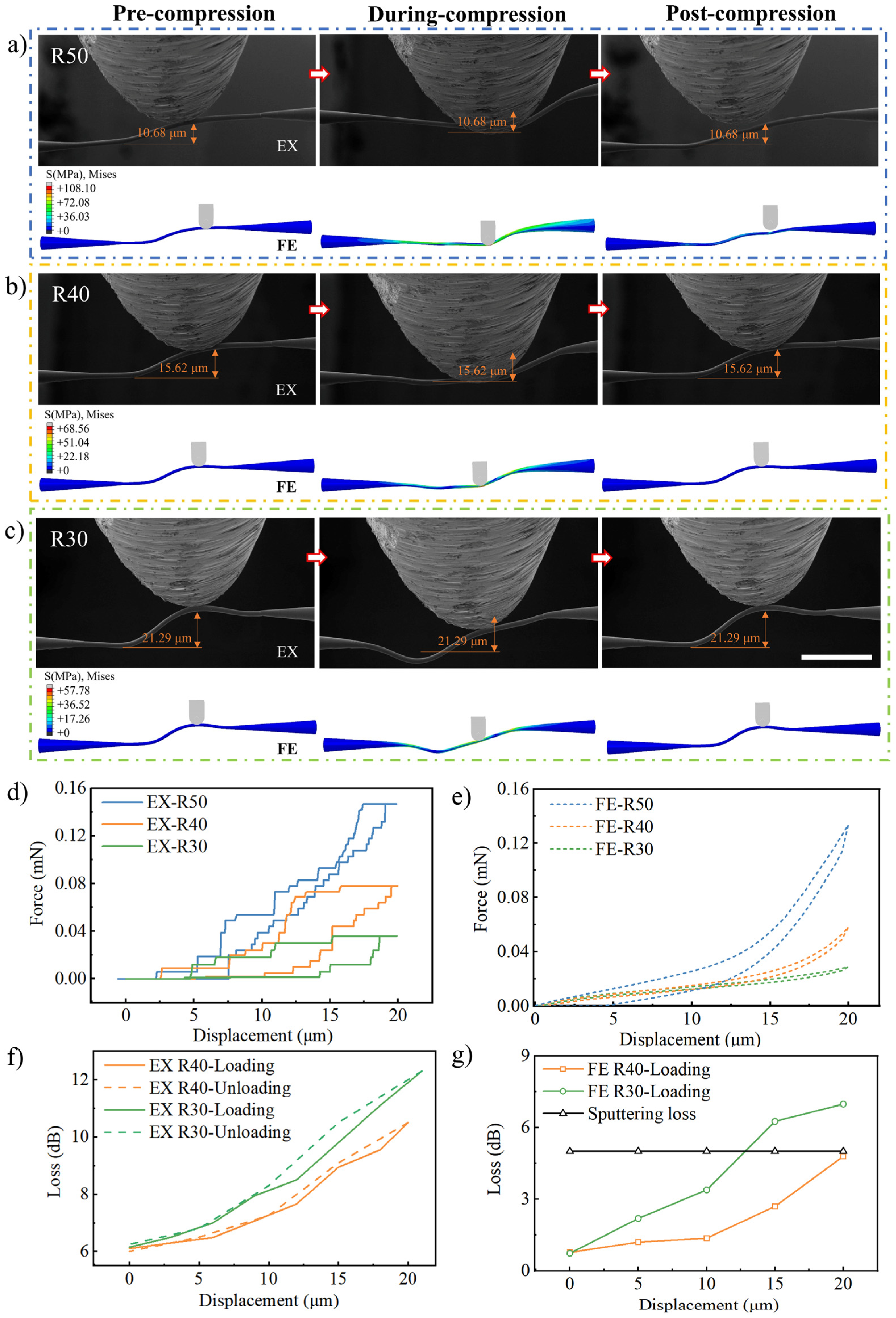
3.4. Mechanical Resilience and Optical Recovery of PWB
4. Conclusions
Supplementary Materials
Author Contributions
Funding
Institutional Review Board Statement
Informed Consent Statement
Data Availability Statement
Conflicts of Interest
References
- Florea, L.; Blasco, E.; Mattoli, V. New Frontiers in Materials and Technologies for 3D Two Photon Polymerization. Adv. Funct. Mater. 2023, 33, 2305697. [Google Scholar] [CrossRef]
- Schwärzle, D.; Hou, X.; Prucker, O.; Rühe, J. Polymer Microstructures through Two-Photon Crosslinking. Adv. Mater. 2017, 29, 1703469. [Google Scholar] [CrossRef] [PubMed]
- Bauer, J.; Guell Izard, A.; Zhang, Y.; Baldacchini, T.; Valdevit, L. Programmable Mechanical Properties of Two-Photon Polymerized Materials: From Nanowires to Bulk. Adv. Mater. Technol. 2019, 4, 1900146. [Google Scholar] [CrossRef]
- Chu, W.; Tan, Y.; Wang, P.; Xu, J.; Li, W.; Qi, J.; Cheng, Y. Centimeter-Height 3D Printing with Femtosecond Laser Two-Photon Polymerization. Adv. Mater. Technol. 2018, 3, 1700396. [Google Scholar] [CrossRef]
- Henning, I.; Woodward, A.W.; Rance, G.A.; Paul, B.T.; Wildman, R.D.; Irvine, D.J.; Moore, J.C. A Click Chemistry Strategy for the Synthesis of Efficient Photoinitiators for Two-Photon Polymerization. Adv. Funct. Mater. 2020, 30, 2006108. [Google Scholar] [CrossRef]
- Han, F.; Gu, S.; Klimas, A.; Zhao, N.; Zhao, Y.; Chen, S.-C. Three-dimensional nanofabrication via ultrafast laser patterning and kinetically regulated material assembly. Science 2022, 378, 1325–1331. [Google Scholar] [CrossRef]
- Burmeister, F.; Zeitner, U.D.; Nolte, S.; Tünnermann, A. High numerical aperture hybrid optics for two-photon polymerization. Opt. Express 2012, 20, 7994–8005. [Google Scholar] [CrossRef]
- Pudis, D.; Goraus, M.; Urbancova, P. Optical properties of woodpile structures for application on the surface of photonic devices. Appl. Surf. Sci. 2018, 461, 227–232. [Google Scholar] [CrossRef]
- Yao, P.; Liu, R.; Broggini, T.; Thunemann, M.; Kleinfeld, D. Construction and use of an adaptive optics two-photon microscope with direct wavefront sensing. Nat. Protoc. 2023, 18, 3732–3766. [Google Scholar] [CrossRef]
- Billah, M.R.; Blaicher, M.; Hoose, T.; Dietrich, P.-I.; Marin-Palomo, P.; Lindenmann, N.; Nesic, A.; Hofmann, A.; Troppenz, U.; Moehrle, M.; et al. Hybrid integration of silicon photonics circuits and InP lasers by photonic wire bonding. Optica 2018, 5, 876–883. [Google Scholar] [CrossRef]
- Lin, B.; Witt, D.; Young, J.F.; Chrostowski, L. Cryogenic optical packaging using photonic wire bonds. APL Photonics 2023, 8, 126109. [Google Scholar] [CrossRef]
- Cai, C.; Wang, J. Femtosecond Laser-Fabricated Photonic Chips for Optical Communications: A Review. Micromachines 2022, 13, 630. [Google Scholar] [CrossRef] [PubMed]
- Juodkazis, S. Laser polymerized photonic wire bonds approach 1 Tbit/s data rates. Light Sci. Appl. 2020, 9, 72. [Google Scholar] [CrossRef] [PubMed]
- Blaicher, M.; Billah, M.R.; Kemal, J.; Hoose, T.; Marin-Palomo, P.; Hofmann, A.; Kutuvantavida, Y.; Kieninger, C.; Dietrich, P.-I.; Lauermann, M.; et al. Hybrid multi-chip assembly of optical communication engines by in situ 3D nano-lithography. Light Sci. Appl. 2020, 9, 71. [Google Scholar] [CrossRef]
- Kiefer, P.; Hahn, V.; Nardi, M.; Yang, L.; Blasco, E.; Barner-Kowollik, C.; Wegener, M. Sensitive Photoresists for Rapid Multiphoton 3D Laser Micro- and Nanoprinting. Adv. Opt. Mater. 2020, 8, 2000895. [Google Scholar] [CrossRef]
- Lindenmann, N.; Balthasar, G.; Hillerkuss, D.; Schmogrow, R.; Jordan, M.; Leuthold, J.; Freude, W.; Koos, C. Photonic wire bonding: A novel concept for chip-scale interconnects. Opt. Express 2012, 20, 17667–17677. [Google Scholar] [CrossRef]
- Gu, Z.; Amemiya, T.; Ishikawa, A.; Atsumi, Y.; Kang, J.; Hiratani, T.; Hayashi, Y.; Suzuki, J.; Nishiyama, N.; Tanaka, T.; et al. Investigation of Optical Interconnection by using Photonic Wire Bonding. J. Laser Micro 2014, 10, 148–153. [Google Scholar] [CrossRef]
- Liang, Y.; Luo, A.; Wang, L.; Hu, S.; Guo, W.; Yao, Y.; Wan, Q. In-situ SEM investigation of low-cycle fatigue behavior and microstructure evolution of CoCrNi medium entropy alloy. J. Mater. Res. Technol. 2023, 25, 1–12. [Google Scholar] [CrossRef]
- Barrios, A.; Kunka, C.; Nogan, J.; Hattar, K.; Boyce, B.L. Automated High-Throughput Fatigue Testing of Freestanding Thin Films. Small Methods 2023, 7, 2201591. [Google Scholar] [CrossRef]
- Wang, X.; Zhao, Y.; Wang, L.; Wei, L.; He, J.; Guan, X. In-situ SEM investigation and modeling of small crack growth behavior of additively manufactured titanium alloy. Int. J. Fatigue 2021, 149, 106303. [Google Scholar] [CrossRef]
- Juri, A.Z.; Basak, A.K.; Yin, L. In-situ SEM micropillar compression of porous and dense zirconia materials. J. Mech. Behav. Biomed. Mater. 2022, 132, 105268. [Google Scholar] [CrossRef] [PubMed]
- Chen, B.; Yang, R.; Dong, J.; Wang, S.; Wang, J.; Huan, Y. Development of in-situ SEM torsion tester for microscale materials. Measurement 2019, 139, 421–425. [Google Scholar] [CrossRef]
- Fritz, R.; Kiener, D. Development and application of a heated in-situ SEM micro-testing device. Measurement 2017, 110, 356–366. [Google Scholar] [CrossRef]
- Cherukuri, R.; Lambai, A.; Sukki, L.; Väliaho, J.; Kallio, P.; Sarlin, E.; Ramachandramoorthy, R.; Kanerva, M.; Mohanty, G. In-situ SEM micropillar compression and nanoindentation testing of SU-8 polymer up to 1000 s−1 strain rate. Mater. Lett. 2024, 358, 135824. [Google Scholar] [CrossRef]
- Rohbeck, N.; Ramachandramoorthy, R.; Casari, D.; Schürch, P.; Edwards, T.E.J.; Schilinsky, L.; Philippe, L.; Schwiedrzik, J.; Michler, J. Effect of high strain rates and temperature on the micromechanical properties of 3D-printed polymer structures made by two-photon lithography. Mater. Des. 2020, 195, 108977. [Google Scholar] [CrossRef]
- Li, Q.; Kulikowski, J.; Doan, D.; Tertuliano, O.A.; Zeman, C.J.; Wang, M.M.; Schatz, G.C.; Gu, X.W.J.S. Mechanical nanolattices printed using nanocluster-based photoresists. Science 2022, 378, 768–773. [Google Scholar] [CrossRef]
- Bauer, J.; Schroer, A.; Schwaiger, R.; Kraft, O. Approaching theoretical strength in glassy carbon nanolattices. Nat. Mater. 2016, 15, 438–443. [Google Scholar] [CrossRef]
- Vlasov, Y.A.; McNab, S.J. Losses in single-mode silicon-on-insulator strip waveguides and bends. Opt. Express 2004, 12, 1622–1631. [Google Scholar] [CrossRef]
- Lindenmann, N.; Dottermusch, S.; Goedecke, M.L.; Hoose, T.; Billah, M.R.; Onanuga, T.P.; Hofmann, A.; Freude, W.; Koos, C. Connecting Silicon Photonic Circuits to Multicore Fibers by Photonic Wire Bonding. J. Light. Technol. 2015, 33, 755–760. [Google Scholar] [CrossRef]
- Park, J.-G.; Lee, S.-H.; Ryu, J.-S.; Hong, Y.-K.; Kim, T.-G.; Busnaina, A. Interfacial and Electrokinetic Characterization of IPA Solutions Related to Semiconductor Wafer Drying and Cleaning. J. Electrochem. Soc. 2006, 153, G811–G814. [Google Scholar] [CrossRef]


Disclaimer/Publisher’s Note: The statements, opinions and data contained in all publications are solely those of the individual author(s) and contributor(s) and not of MDPI and/or the editor(s). MDPI and/or the editor(s) disclaim responsibility for any injury to people or property resulting from any ideas, methods, instructions or products referred to in the content. |
© 2024 by the authors. Licensee MDPI, Basel, Switzerland. This article is an open access article distributed under the terms and conditions of the Creative Commons Attribution (CC BY) license (https://creativecommons.org/licenses/by/4.0/).
Share and Cite
Lei, Y.; Sun, W.; Huang, X.; Wang, Y.; Gao, J.; Li, X.; Xiao, R.; Deng, B. In Situ Multiphysical Metrology for Photonic Wire Bonding by Two-Photon Polymerization. Materials 2024, 17, 5297. https://doi.org/10.3390/ma17215297
Lei Y, Sun W, Huang X, Wang Y, Gao J, Li X, Xiao R, Deng B. In Situ Multiphysical Metrology for Photonic Wire Bonding by Two-Photon Polymerization. Materials. 2024; 17(21):5297. https://doi.org/10.3390/ma17215297
Chicago/Turabian StyleLei, Yu, Wentao Sun, Xiaolong Huang, Yan Wang, Jinling Gao, Xiaopei Li, Rulei Xiao, and Biwei Deng. 2024. "In Situ Multiphysical Metrology for Photonic Wire Bonding by Two-Photon Polymerization" Materials 17, no. 21: 5297. https://doi.org/10.3390/ma17215297
APA StyleLei, Y., Sun, W., Huang, X., Wang, Y., Gao, J., Li, X., Xiao, R., & Deng, B. (2024). In Situ Multiphysical Metrology for Photonic Wire Bonding by Two-Photon Polymerization. Materials, 17(21), 5297. https://doi.org/10.3390/ma17215297