Article

Titanium Dioxide Thin Films Produced on FTO Substrate Using the Sol–Gel Process: The Effect of the Dispersant on Optical, Surface and Electrochemical Features

by
Vasilica Mihaela Mîndroiu
*,
Andrei Bogdan Stoian
,
Roberta Irodia
,
Roxana Trușcă
and
Eugeniu Vasile
Faculty of Chemical Engineering and Biotechnologies, University Politehnica of Bucharest, 1-7 Polizu, 011061 Bucharest, Romania
*
Author to whom correspondence should be addressed.
Materials 2023, 16(8), 3147; https://doi.org/10.3390/ma16083147
Submission received: 26 March 2023 / Revised: 12 April 2023 / Accepted: 14 April 2023 / Published: 16 April 2023

Abstract

:
In this study, TiO2 thin films formed by dip-coating on an FTO substrate were obtained and characterized using surface, optical and electrochemical techniques. The impact of the dispersant (polyethylene glycol-PEG) on the surface (morphology, wettability, surface energy), optical (band gap and Urbach energy) and electrochemical (charge-transfer resistance, flat band potential) properties were investigated. When PEG was added to the sol–gel solution, the optical gap energy of the resultant films was reduced from 3.25 to 3.12 eV, and the Urbach energy increased from 646 to 709 meV. The dispersant addition in the sol–gel process influences surface features, as evidenced by lower contact-angle values and higher surface energy achieved for a compact film with a homogenous nanoparticle structure and larger crystallinity size. Electrochemical measurements (cycle voltammetry, electrochemical impedance spectroscopy and the Mott–Schottky technique) revealed improved catalytic properties of the TiO2 film, due to a higher insertion/extraction rate of protons into the TiO2 nanostructure, as well as a decrease in charge-transfer resistance from 418 k to 23.4 k and a decrease in flat band potential from 0.055 eV to −0.019 eV. The obtained TiO2 films are a promising alternative for technological applications, due to their advantageous surface, optical and electrochemical features.

1. Introduction

Titanium dioxide (TiO2) thin films with high specific surface area and narrow pore-size distribution have piqued the interest of industry professionals due to their excellent optical, electrical, and photoelectrochemical properties [1]. TiO2 is a nontoxic material with wide band gap in its three crystalline forms: rutile (tetragonal), anatase (tetragonal), and brookite (orthorhombic) [2]. Among these, the anatase phase of TiO2 has sparked interest among scientists in a variety of fields, due to its potential use in catalysis and photo-catalysis [3,4] for air and water clearing and also in water splitting [5] and in organic pollutant degradation [6], energy storage and solar energy conversion [7,8], electrochromic and self-cleaning smart windows [9,10] and in biomedical applications [11,12]. The synthesis method, experimental settings, sol composition [13] and polymorph structure are just a few of the variables that affect the properties of TiO2 nanoparticles [14,15]. Chemical vapor deposition (CVD) [16], radio frequency (RF) magnetron sputtering (SPS) [17], nebulized spray deposition [9] and the sol–gel procedure [18] are only some of the more common methods currently used to create anatase TiO2 thin films. The sol–gel approach is the most appealing of the mentioned methods, due to the simplicity of the required equipment, low processing temperature, good homogeneity, and the ability to achieve multilayer deposition [19] on different substrates, including metals [20], indium-doped tin oxide (ITO) [21] or fluorine-doped tin oxide (FTO) glass [9], depending on the application area.
Thus far, the impact of different conditions on the structural and optical features of TiO2 thin films has been the subject of numerous investigations. As an example, F. Zeribi et al. investigated how the number of layers affected the physical characteristics of TiO2 that were applied to a glass substrate using the sol–gel spin coating process [18]. N. Barati et al. demonstrated that the withdrawal speed used for the dip-coating process influences the coating thickness, and a drying method for coatings is required to achieve a uniform and nanocrystalline TiO2 coating on 316L stainless steel [20]. Other studies investigated the effect of the additive and annealing temperatures on the surface morphology of spin-coated TiO2 thin films [22,23,24]. To change the morphology and crystallinity, some complex agents (such as acetylacetone, diethanolamine, polyethylene glycol, Lauryl lactyl lactate) [25,26] or surfactants (such as cationic-sodium dodecyl sulphate (SDS), cetyltrimethylammonium bromide (CTAB), and non-ionic (TritonX-100)) [27] were added. As a result, particle agglomeration was reduced and TiO2 coating stability and photocatalytic efficiency were improved. Moreover, when two or more distinct surfactants were introduced to the mixture simultaneously, the morphology of TiO2 changed substantially, adopting spherical and three-dimensional forms because of surfactant coordination [27].
Efforts are still being made to obtain adherent and continuous TiO2 films on FTO or ITO glass electrodes with improved optical properties in the visible range, as well as improved electrochemical and electrochromic properties, with the goal of using these electrodes in cutting-edge applications, such as smart windows, which are of great interest today, given global warming and the energy crisis.
This study determines the optimal number of dip-coating layers and the effect of the dispersant (PEG) added to the sol–gel precursor solution on the optical (as reduced band gap and increased Urbach energies), electrochemical (as high insertion/extraction rate of protons, decrease in charge-transfer resistance, and flat band potential) and surface (nanomorphology, crystallinity, decreased wettability and high surface energy) properties of titanium dioxide thin films obtained on FTO.
The results of this research will help to develop a practical procedure to create pseudo-capacitive electrodes for technological applications by correlating the surface morphology, vibrational, and optical properties of synthesized TiO2 thin films on FTO substrates with electrochemical properties.

2. Experimental Techniques

2.1. Materials

Titanium butoxide (Ti(OBu)4 (Bu = CH2CH2CH2CH3)), anhydrous ethanol (C₂H₆O), acetic acid (CH3COOH), polyethylene glycol 8000 (PEG), sulphuric acid (H2SO4) (Alfa Aesar, Haverhill, MA, USA), ≥99.5% ethylene glycol (Honeywell, Charlotte, NC, USA), acetyl acetone (CH₃COCH₂COCH₃) (Sigma Aldrich, Saint Louis, MO, USA), dimethyl sulfoxide (DMSO) (Carlo Erba Reagents, Cornaredo, MI, Italy) and distilled water were used as reagents in the present work. The TiO2 films with different thicknesses were deposited on fluorine-doped tin oxide (FTO; Rsh = 15 Ω/sq; 2.5 × 5 cm2, 1.3 mm thickness, Solaronix, Aubonne, Switzerland) coated glass substrates.

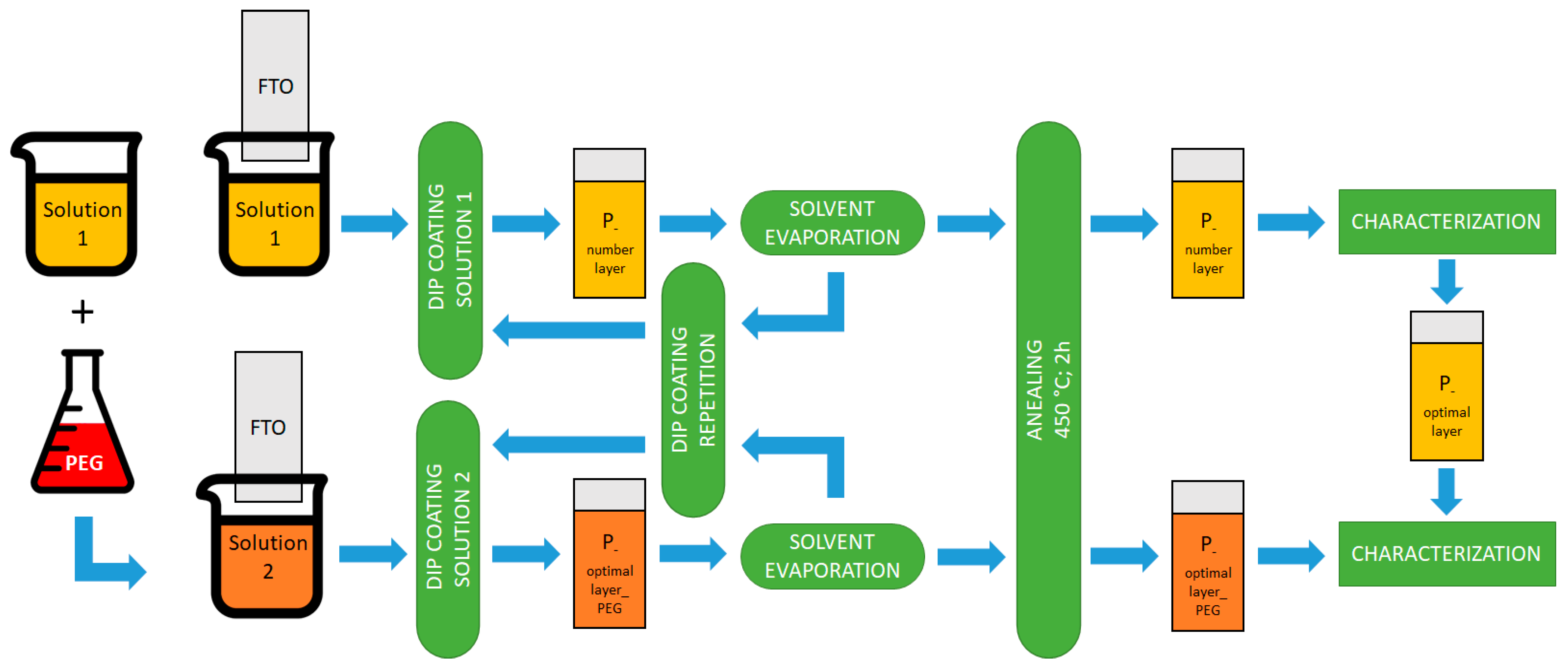
2.2. Preparation of TiO2 Thin Films on FTO Substrate by Dip-Coating Method

The sol–gel precursor solution (Solution 1) was created by mixing together 8 mL Ti(OBu)4, (as alkoxide), 80 mL ethanol (as solvent), 8 mL acetylacetone (as catalyst), 8 mL CH3COOH (as pH adjuster, to 6) and 8 mL of water [18,28]. A clear solution was obtained after 3 h of stirring the mixture at 50 °C, which was further aged for 24 h at room temperature. The FTO substrates were cleaned with ethanol, acetone, and distilled water for ten minutes each, then dried in air.
The precursor solution was set up by dip-coating onto the surfaces after they had been cleaned using a KSV NIMA Dip-Coater (Biolin Scientific, Västra Frölunda, Sweden) using the following parameters: immersion speed 3 cm/min, immersion time 30 s and lifting speed 10 cm/min. The resulting film was dried in an oven at 200 °C for 10 min after each deposition cycle for the organic solvent evaporation. To obtain films with different thicknesses, the deposition procedure was repeated 2, 4, 6 and 8 times. The names of the samples obtained by this method are listed as “Pnumber layer”. Then, the obtained films were investigated to determine the ideal number of layers needed to generate a TiO2 film with a lower band gap energy and higher Urbach energy.
After determining the optimal number of TiO2 layers, we investigated how the presence of a dispersant in the precursor solution influences the nanomorphology of the material, electrochemical and optical properties of the resulting TiO2 film. In order to accomplish this, a second solution identified as Solution 2 was made by continuously stirring Solution 1 for a period of two hours, until a specific amount of PEG was dissolved [29]. PEG promotes nanopore formation and reduces TiO2 nanoparticle aggregation [30]. The names of the samples that were obtained using this method are identified as follows: “Pnumber layer_PEG”.
All films obtained from both solutions were annealed in an electric furnace for two hours at 450 °C.
The stages involved in TiO2 thin film production are depicted in Figure 1.

2.3. Characterization Methods

2.3.1. The Optical Properties

The band gap energy, transmittance and Urbach energy of TiO2 films obtained on FTO from Solution 1 and Solution 2, were calculated taking UV–Vis light transmittance measurements in the wavelength range of 300–800 nm, using a Perkin Elmer Lambda (Waltham, MA, USA) 650/850/950 UV/Vis spectrophotometer. These studies were carried out three times each, highlighting a minimum statistical and standard deviation in the data.

2.3.2. Physicochemical Characterization

The crystal structure of the TiO2 films was examined with the Panalytical (Malvern, UK) X’Pert Pro MPD X-ray diffractometer, using a CuK α X-ray beam (wavelength 1.54065 Å) and Bragg–Brentano geometry. The effects of the dispersant present in sol–gel dip-coating solution on the microstructure and morphology of the TiO2 thin films were investigated using the QUANTA INSPECT F50 (FEI Company, Eindhoven, The Netherlands) scanning electron microscope equipped with a field emission gun (FEG) with a resolution of 1.2 nm and an energy dispersive X-ray spectrometer (EDS) with MnK resolution of 133 eV. The size of the particles were determined using Image J software; at least 10 measurements were performed on SEM images and then the average and standard deviation were calculated. The surface analysis and roughness evaluation were performed using an atomic force microscope (AFM) (APE Research, Trieste, Italy), in contact mode. Structural and chemical bonding of TiO2 films were studied via infrared spectroscopy using a Perkin Elmer (Waltham, MA, USA) Spectrum 100 FT-IR spectrometer in the attenuated total reflection mode (ATR). ATR/FT-IR spectra were recorded in the 4000 cm−1–600 cm−1 domain, representing an average of 4 scans collected at a resolution factor of 4 cm−1. The contact angle measurements completed the surface characterization, quantifying the wettability of a solid surface by a liquid and calculating the surface free energy. Thus, the sessile drop technique was used with three different solvents: distilled water, Ethylene Glycol (EG), and dimethyl sulfoxide (DMSO) to determine the contact angle using an optical contact angle measuring instrument (Contact Angle Meter—KSV Instruments CAM 100 equipment) (Biolin Scientific, Västra Frölunda, Sweden).

2.3.3. Testing of Electrochemical Properties

Cyclic voltammetry (CV), electrochemical impedance spectroscopy (EIS) and Mott–Schottky measurements were carried out from −0.6 V to +0.2 V domain range in 0.5 M H2SO4 aqueous solution, to investigate the electrochemical stability and the interfacial charge-separation efficiencies of the TiO2 film as a function of the dispersant presence in sol–gel dip-coating solution. The procedures below were carried out using a three-electrode electrochemical cell: the obtained electrodes were the working electrodes Ag/AgCl, KCl sat. and Pt mesh as reference and counter electrodes, respectively. An Autolab (PGSTAT 204) potentiostat/galvanostat from Metrohm (Herisau, Switserland) system was used to control the parameters as well as collect data.

3. Results and Discussions

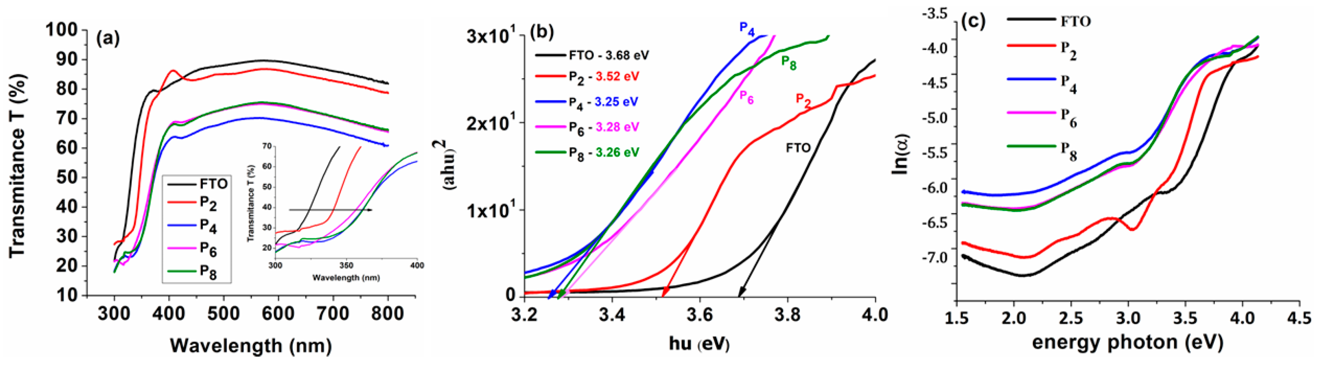
3.1. Determining the Optimum Number of Dip-Coatings Required to Deposit the TiO2 Film on the FTO Substrate with the Lowest Band-Gap and Highest Urbach-Energy Values

In the research carried out on the mechanism of thin film growth, three distinct phases of film creation are typically identified and discussed: (1) nucleation, (2) cross linking and (3) vertical growth [18]. The substrate temperature determines the onset and rate of the first two phases, whereas the amount of layer deposition, or film thickness, governs the vertical growth phase. Hence, the source of surface roughness and agglomeration and clusters on the top surface may be traced back to the vertical growth, also known as columnar growth. Thus, the number of layers used for TiO2 dip-coating deposition onto the FTO substrate influences surface properties such as roughness and optical features.
According to the AFM image in Figure 2a, the TiO2 film produced by two cycles of dip-coating exhibited both tubular and palletized morphologies. The tube dimensions are around 3–5 µm in length and 0.65 µm in width and the pallet constructions have side lengths of 1.4 µm and 0.7 µm. The structures’ heights range from 100 to 200 nm.
The topography of the formed film by four dip-coating cycles on the FTO substrate (Figure 2b) shows that the FTO substrate is completely covered by intricate TiO2 structures. The TiO2 structures are irregular clusters of around 1–2 µm in length and 200–400 nm in height. The TiO2 films formed by six and eight cycles of dip-coating deposition on FTO (Figure 2c,d) completely cover the substrate with irregular TiO2 dome-like structures of 3 µm in width and heights ranging from 400 to 700 nm. The topography of the FTO substrate on which the TiO2 films were deposited by dip-coating (Figure 2e) reveals that the FTO (fluorine-doped tin oxide) particles are granular in appearance and uniformly cover the glass substrate, with grain diameters ranging from 10 to 50 nm and heights from 10 to 25 nm.
The thickness and roughness of the TiO2 films obtained by various dip-coating deposition cycles on the FTO substrate are shown in Table 1.
The TiO2 film deposition on the FTO substrates from Solution 1 results in thick layers, with thicknesses ranging from 0.674 µm for two layers to 1.945 µm for eight layers. Once many layers are deposited onto the substrate, the thickness increases as reported in the literature [18,31,32], and microcracks begin to emerge on the surface (as seen in AFM pictures corresponding to six and eight layers). Findings from other studies suggest that internal stresses are generated as the density of nucleation centers decreases with layer thickness [33,34], leading to increased surface microcracks [35]. We expect all these factors to affect the films’ optical characteristics of samples with the most layers deposited.
The optical transmittance spectra of TiO2 thin films deposited from Solution 1 on the FTO substrate in the wavelength range of 300–800 nm are shown in Figure 3a as a function of the number of dip-coating layers.
The inset of Figure 3a shows that once the number of layers increases, the edge of absorption shifts to longer wavelengths as time passes, indicating that the band energy of the films formed on the FTO substrate is reducing. Furthermore, increasing the number of layers of the film makes it thicker and reduces its transmittance. The electronic transition between the TiO2 valence band and conduction band induces fundamental light absorption in the TiO2 thin films, as shown in the transmittance spectrum (Figure 3a) at 407 nm [36]. In addition, for all obtained films, a high transmission region (over 60%) was found in the visible zone (500–800 nm), indicating anti-reflection and UV-protective properties [37].
Plotting curves between (αhν)2 and (hν) yields the optical energy of the band gap of the TiO2 film produced on the FTO substrates after two, four, six, and eight dip-coating cycles (Figure 3b). The band gap energy is determined using Tauc’s equation with the following relationship [38]:
(αhν) = A(hν − Eg)
where Eg is the bandgap energy, A is a constant, hν is the energy of the incident photon and α is the absorption coefficient [39].
The band gap value decreases with the increasing number of dip-coating deposition cycles, remaining nearly constant after four deposition cycles, at around 3.26 eV ± 0.2 eV.
Defects in the film lattice in the optical band gap region are represented by the Urbach energy (band tail width), (Eu), in Figure 3c. The Urbach tail, or absorption tail, can be traced back to flaws in the forbidden band region. The following formulas were used to calculate the Urbach energy from the absorption spectrum [40]:
α = α 0 e x p h υ E u   and   E u = d [ α h υ ] d [ h υ ] 1
where α0 is a constant and Eu is the Urbach energy.
The Urbach energy is estimated from the graph ln(α) = f (photon energy) (Figure 3c): Eu = 1/Slope. Table 2 displays the computed band gap energy and Urbach energy of the TiO2 thin films after two, four, six, and eight dip-coating cycles.
The band gap energy (Eg) is found to decrease from 3.52 eV to 3.25 eV as the number of layers increases, while the Urbach energy increases from 310 meV to 646 meV. Based on the AFM results, it can be observed that, due to the appearance of many microcracks in P6 and P8, the band gap slowly increased and Urbach energy decreased, compared with sample P4, which presented a uniform compact film.
These findings are consistent with previous research [41,42,43]. Band gap energy values of TiO2 thin layers formed on the glass substrate by sol–gel spin coating were calculated to be between 3.67 and 3.52 eV in earlier research [18]; however, the obtained band gap energy values range from 3.52 to 3.25 eV of the TiO2 coated by sol–gel dip-coating on the FTO substrate.
Furthermore, cyclic voltammetry (CV) was performed to examine the relationship between the number of layers and the adherence of the obtained TiO2 layers on the FTO substrate (Figure 4). Thus, 100 CV cycles were recorded for all samples, to determine the electrochemical stability of the films on the FTO substrate. Results are illustrated in Figure 4. As the number of CV cycles grew, the corresponding constant current values for P4 indicated (Figure 4b) a strong bond on the substrate and good electrochemical stability [44].
The greater the film’s electrochemical stability, the better it adheres to the substrate. Samples of both types, P2 and P4, are stable, with P4 showing a more capacitive behavior. In the samples of P6 and P8, the results changed substantially after almost 20 CV cycles. Microcracks in samples P6 and P8 cause an unstable CV signal and a higher optical transmittance compared to sample P4, as shown by a correlation between the CV test results, the AFM results, and the optical properties.
This phenomenon keeps these films unstable even as they increase in thickness and develop microcracks. Electrolytes infiltrate through microcracks between the films and the substrate, causing the current to fluctuate as the CV cycles increase.
Based on the current experimental results, it has been concluded that four-cycle dip-coating is the ideal approach for depositing TiO2 multilayers onto FTO substrates, because it has the best optical properties and because it presents electrochemical stability.

3.2. Evaluating the Impact of the PEG Presence in the Sol–Gel Precursor Solution on the Morphological, Optical and Electrochemical Properties of TiO2 Films

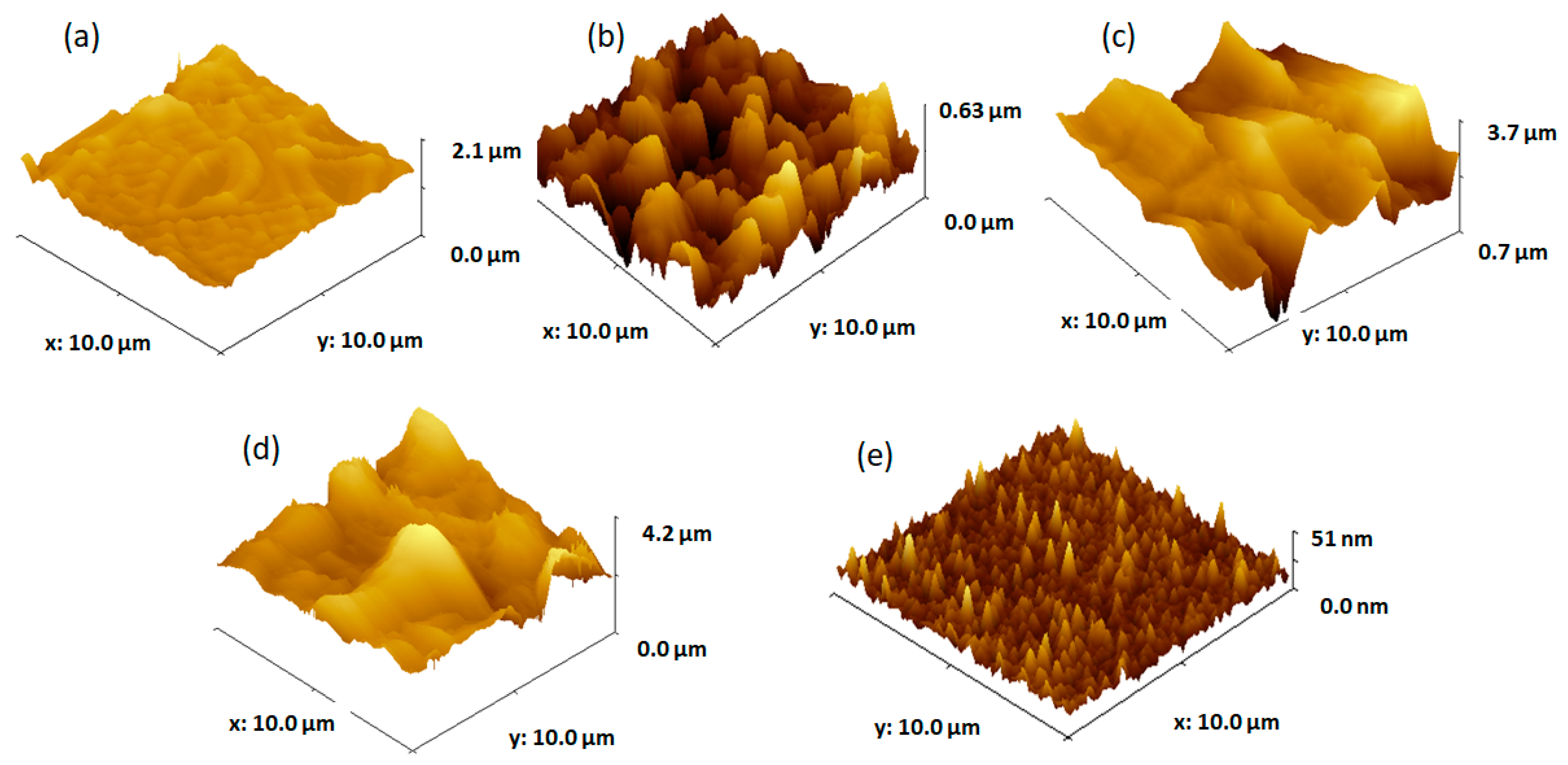
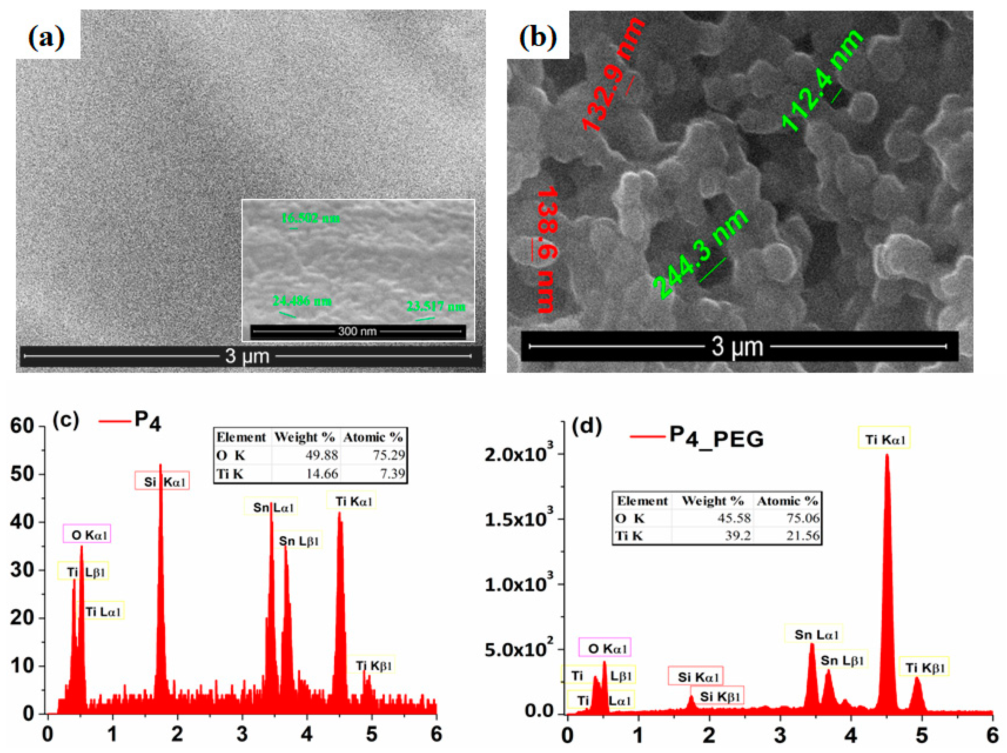
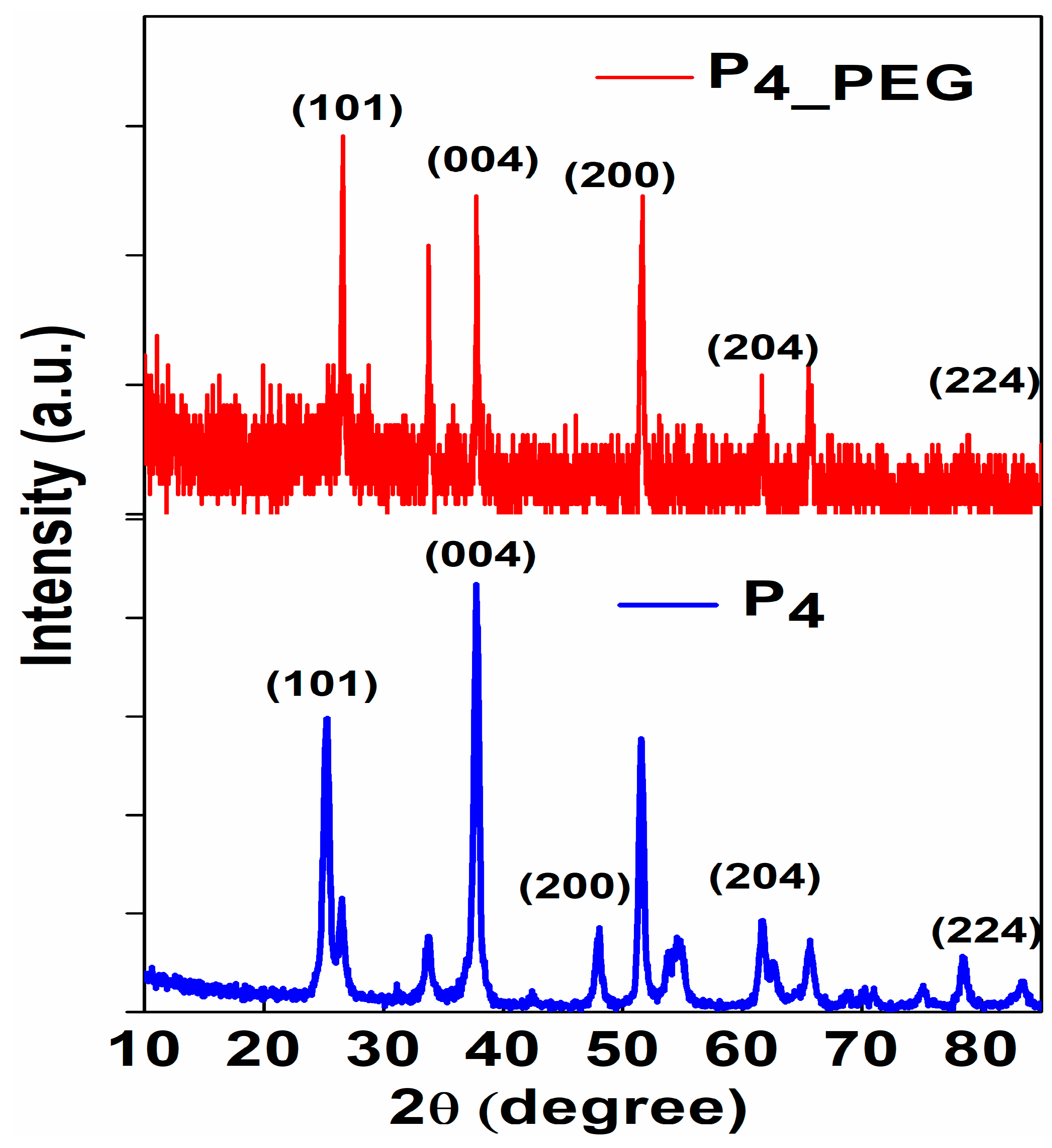
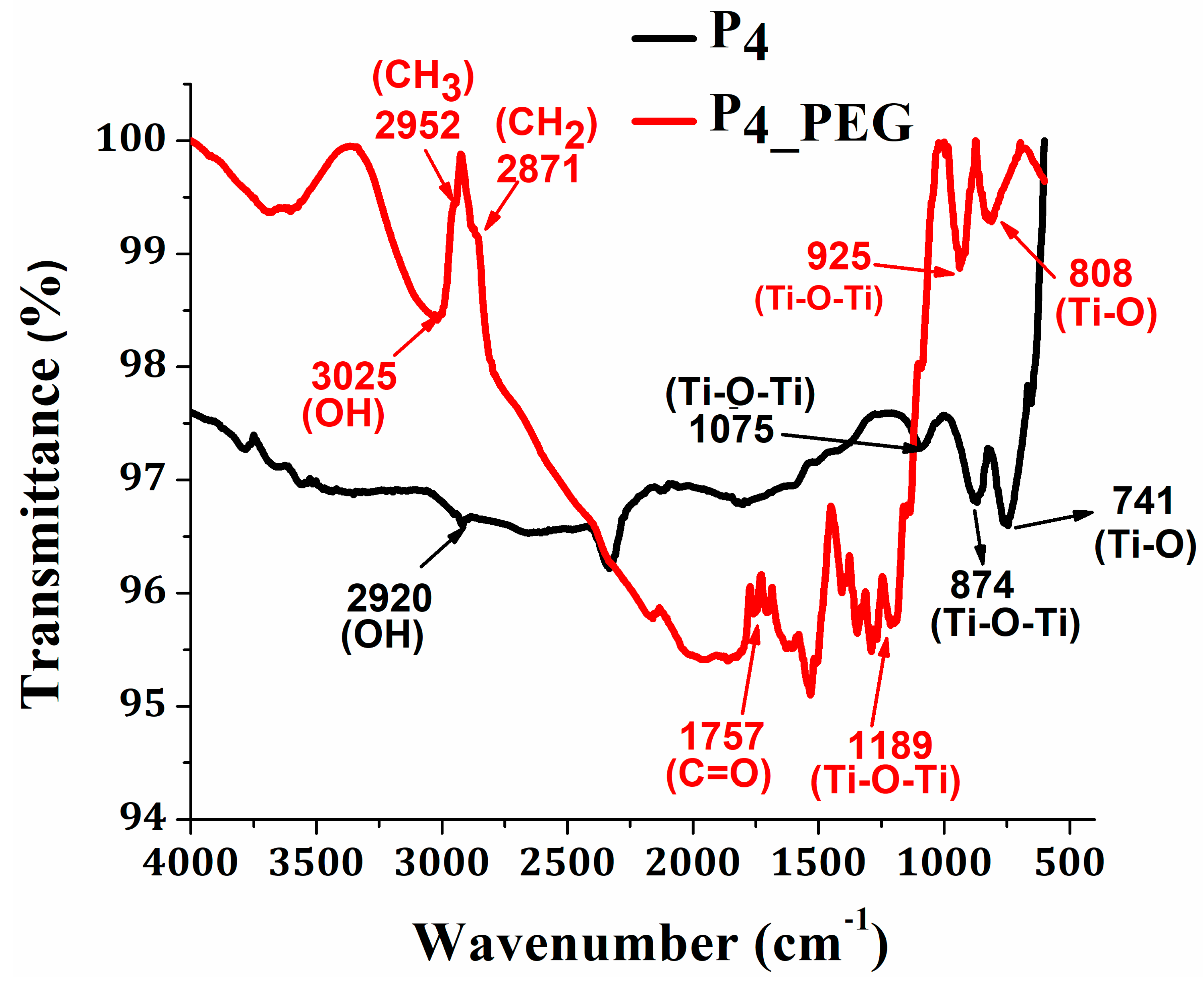
3.2.1. Surface Characterization

Given the band gap and Urbach energy results, from which we have determined that the samples with four TiO2 layers conferred the best results, henceforth, all the presented data represent the results obtained for the samples obtained after four dip-coating cycles in Solution 1 and in Solution 2.
The SEM image (Figure 5a) obtained for the surface of the P4 film indicates a compact and uniform TiO2 thin layer with a homogeneous distribution of nanoparticles with an average size of around 23 nm (±2.93), which covers the whole FTO surface.
Conversely, the morphology of the P4_PEG films (Figure 5b) shows the FTO substrate covered by a continuous TiO2 film with a homogeneous distribution of nanoparticles with an average size of around 100 nm (±6.85). As in the literature [30], the addition of PEG in the coating solution promoted the growth of a nanostructured film and enhanced the production of nanoparticles.
These SEM results demonstrate that the dispersant can modify the size and shape of TiO2 nanoparticles deposited on the FTO substrate by the dip-coating method.
To confirm the presence of both Ti and O in the films obtained from both solutions, the EDX spectra (Figure 5c,d) was performed and recorded. Oxygen is present in nearly equal amounts in both films, while Ti is more abundant in the P4_PEG film.
The crystalline phase and grain size of the films dip-coated on FTO were investigated using X-ray diffraction patterns (Figure 6).
The characteristic peaks at 26.50° and 26.56°; 37.78° and 37.81°; 48.03° and 47.93°; 62.70° and 61.55°; and 83.48° and 84.33°, corresponding to the (101); (004); (200); (204) and (224) planes of TiO2 anatase, respectively, were observed in both the P4 and P4_PEG thin films [45,46]. All the samples exhibited a majority crystallite structure of the TiO2 anatase phase, and the rutile phase was observed at 53.72° and 51.56°, corresponding to the (105) plane, and at 55.10° and 54.54°, corresponding to the (211) plane, for both obtained films.
The average crystallite size (D) of the samples was calculated using the Debye–Scherrer equation [18]:
D = 0.94 λ β cos θ
where θ is the Bragg diffraction angle, λ is the light wavelength utilized for diffraction, equal to 1.54065 Å, and β is the full width at half maxima (FWHM) of the diffraction peak, in radians.
The following relationships were also used to calculate the lattice strain (ε) [47] and dislocation density ( δ ) [48]:
ε = β 4 tan ( θ ) a n d δ = 1 D 2
In Table 3, the variation of crystallite size, the lattice strain and dislocation density are presented.
PEG in solution 2 increases the crystallite size while decreasing the strain, and it is expected to influence optical properties in relation to the band gap’s low energy [18]. This could be due to the relatively easy decomposition of PEG 8000’s high molecular chains during thermal treatment at 450 °C, resulting in the collective fusion of small crystallites into nanoparticle aggregates [15].
Furthermore, the ATR/FT-IR spectra of the TiO2 thin films prepared from solution 1 without a dispersant and solution 2 with PEG were examined using infrared spectroscopy to determine the type of structural and chemical bonding of TiO2 (Figure 7). In both spectra, peaks in the 2920 cm−1 and 3025 cm−1 regions [18,49] are observed and are associated with the stretching vibration of hydroxyl groups. The absorption peaks at 2952 cm−1, 2871 cm−1, and 1757 cm−1 correspond to the stretching vibrations of the CH3, CH2, and C=O groups, respectively, of the PEG from the P4_PEG film [50]. The Ti-O-Ti bonds in the TiO2 nanoparticles’ stretching vibration mode are responsible for the absorption bands at 1075 cm−1 and 874 cm−1, which correspond to P4 [18,51]. The film with PEG presents the same Ti-O-Ti stretching vibration mode, but it is shifted to 1189 cm−1 and 925 cm−1 for the P4_PEG film. The stretching vibration of the Ti-O groups in the anatase phase [18,52] was found at 741 cm−1 and 662 cm−1 for P4 and at 808 cm−1 and 601 cm−1 for P4_PEG [30].
As expected, results from Table 4 indicate that thin TiO2 films displayed low contact angle values due to the hydrophilic nature of the mixture components coated on the substrate. The PEG presence in the sol–gel solution influences the wettability of the obtained TiO2 thin film; the contact angle value (CA = 16°) of the film with a dispersant is lower than the one corresponding to the film without a dispersant (CA = 26°).
Surface free energy, which is a result of film surface defects [53], is important for the pseudo-capacitive processes that occur in many applications such as smart windows. The results of this study indicate that the TiO2 films’ surface free energy varies with the addition of the dispersant. The Owens–Wendt–Rabel–Kaelble (OWRK) model was successfully applied to calculate the surface free energy [54]. In terms of contact angles, the lower the surface energy, the greater the contact angles.

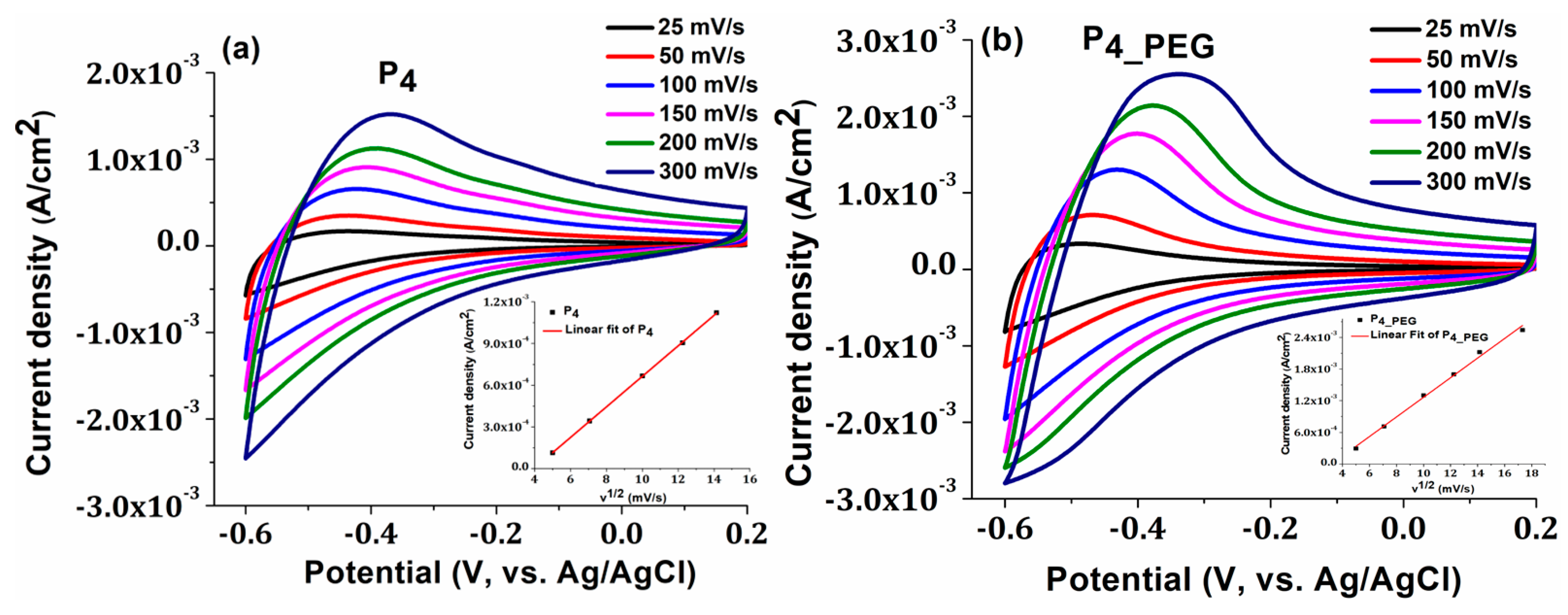
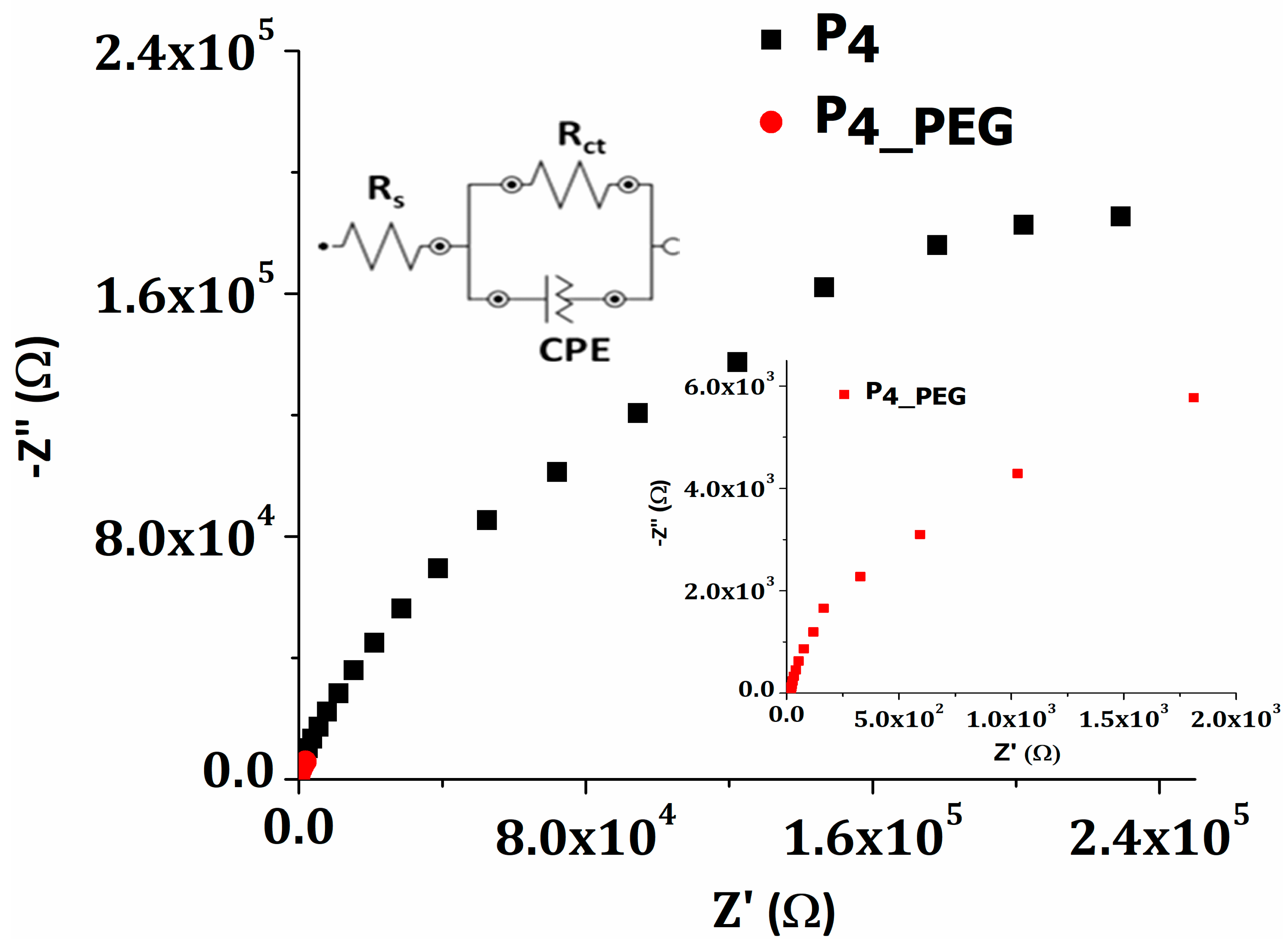
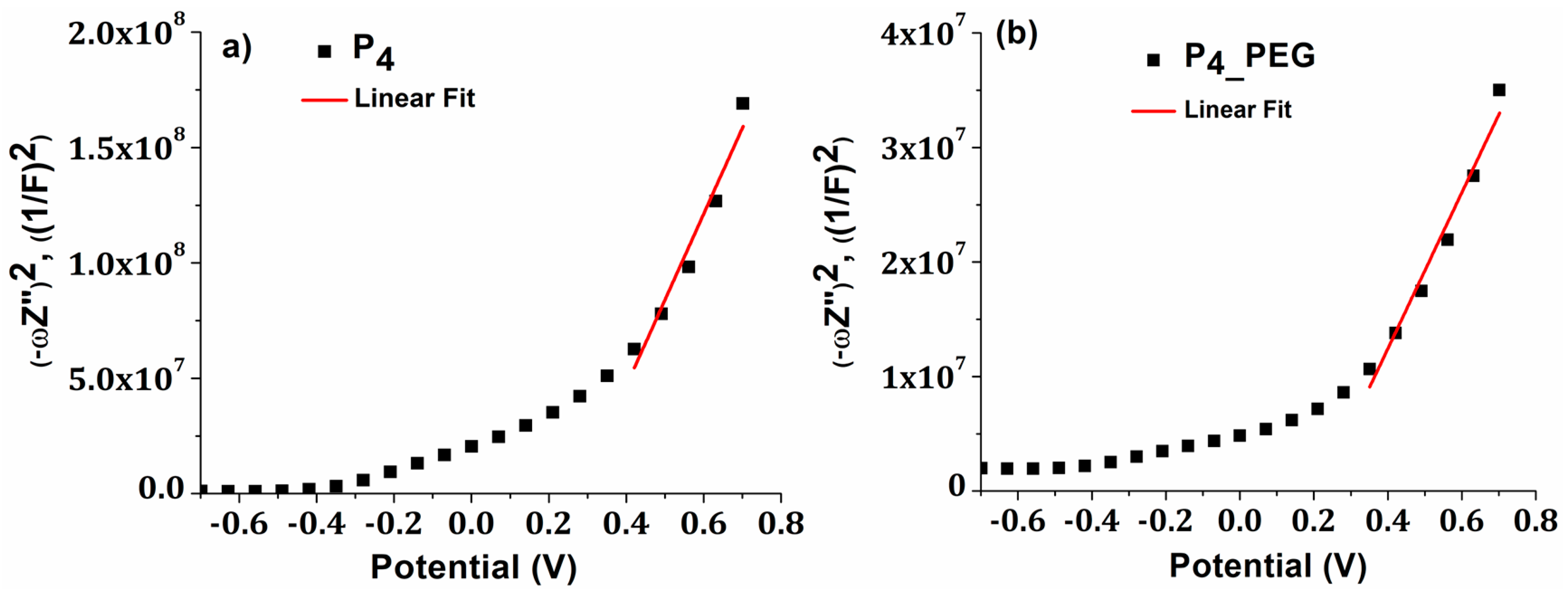
3.2.2. Electrochemical Characterization

The electrochemical behavior of TiO2 films in 0.5 M H2SO4 solution was investigated during the cycling of applied potentials ranging from −0.6 to +0.2 V at different scan rates of 25, 50, 100, 150, 200, and 300 mV s−1. Both obtained films exhibited an oxidation peak near to the Fermi level of anatase TiO2 at −0.5 V (Figure 8) [9]. At rates greater than 50 mV/s, the oxidation peak shifts to less-negative potential values of −0.4 V, due to the oxidation of Ti3+ to Ti4+, because of the deintercalation of H+ ions and electrons from TiO2 nanostructures via the reaction outlined below [55]:
TiO2 + xe + xH+ → TiOOH
A shift in peak potentials toward higher positive values indicates a desirable behavior for the utilization of these electrodes in technological applications with catalytic behavior, such as smart windows.
Moreover, the capacitive behavior of the TiO2 films obtained in the presence of the dispersant is more prominent, and the current density increases, indicating a more conductive character than the film obtained without PEG. Straight lines are obtained when the peak value of the oxidation current is plotted against the square root of the scan speed for both samples (inset Figures), indicating that the insertion and extraction of H+ ions is rapid and that proton diffusion in the TiO2 nanostructure controls the rate-determining step of the redox reaction. Due to the nanocrystalline form of the grains, according to the SEM image (Figure 5b), the diffusion and charge-transfer process of H+ ions in the TiO2 thin film may be facilitated, which may explain why greater charge densities were reported in the P4_PEG thin film [9].
To investigate the charge-transfer kinetics and mass transport behavior of the films developed on the FTO substrate, electrochemical impedance spectroscopy (EIS) analysis was performed. The EIS measurements were made in a frequency range of 10 mHz to 100 kHz. Figure 9 shows the Nyquist plots of the P4 and P4_PEG thin films measured at free potential voltage in 0.5 M H2SO4 solution.
To fit the data, the Randles equivalent circuit model was used, as can be seen in the inset of Figure 9. The equivalent circuit consists of solution resistance (Rs), charge-transfer resistance (Rct) across the developed electrodes/H2SO4 electrolyte interface, and a constant phase element (CPE) which represent a double-layer capacitance at the electrode surface. Table 5 shows the electric parameters from the EIS experimental data fitted with the proposed equivalent circuit.
The charge-transfer resistance (Rct) of the P4 and P4_PEG films deposited on the FTO by dip-coating is 418 kΩ and 23.4 kΩ, respectively. As previously noted, the higher surface free energy, as well as the smaller band gap and higher Urbach energy of the film, produce low charge-transfer resistance, which provides less resistance for ion transport and the slowest recombination rate. When TiO2 was doped with PEG, the density of the nanoparticles in the film increased, leading to higher conductivities. PEG is a well-known long-chain surfactant that helps prevent TiO2 agglomeration during the dip-coating deposition process [56]. The higher value obtained for the P4 film, indicating poor charge-transfer characteristics, is improved by adding PEG to the sol–gel precursor solution. The double-layer capacity of the P4_PEG film is three orders of magnitude greater than that of the TiO2 film prepared from solution 1. Both films exhibited pseudo-capacitive behavior as a result of n values ranging from 0.8 to 1 [57].
The Mott–Schottky (M-S) Equation (5) was used for further analysis of the impedance data and is defined as follows:
1 C 2 = 2 q ε ε 0 N D E E f b k T q
where C is the capacity of the space charge layer, q is the elementary charge, ε0 is the vacuum permittivity, ε is the dielectric constant, ND is the concentration of donors, E is the applied external bias, Efb is the flat band potential, k is Boltzmann’s constant, and T is the absolute temperature.
Flat band potential (Efb) is determined by extrapolating to 1/C2 = 0, which is dependent on the recombination process and interface charge-transfer [58], whereas the slope of the Mott–Schottky plot indicates the doping level (ND). Indirect electron tunnelling through a semiconductor is a well-known result of a band gap with a large concentration of numerous donor levels.
Each P4 and P4_PEG film displayed a positive slope on the Mott–Schottky graphs, as is typical for n-type semiconductors [59], (Figure 10).
Efb is typically regarded as the conduction band potential (CB) for n-type semiconductors [59]. The calculated value of Efb vs. NHnE (normal hydrogen electrode) for P4 and P4_PEG is 0.055 eV and −0.019 eV, respectively. These results imply a slower recombination rate for film formed in the presence of a dispersant, which agrees with the reduction in charge-transfer resistance measured by EIS. The negative shift in the flat-band potential for P4_PEG suggests that the energy barrier for interfacial electron transport is reduced, resulting in a lower charge-transfer resistance [60]. Moreover, the doping level (ND) for P4 and P4_PEG are 6.5 × 1019 cm−3 and 2.01 × 1020 cm−3, respectively, correlating with the variation in Urbach energy values. We may conclude that adding PEG to the sol–gel precursor solution induces a shift in the flat band potential of TiO2 to negative values, indicating improved catalytic capabilities and a higher doping level.

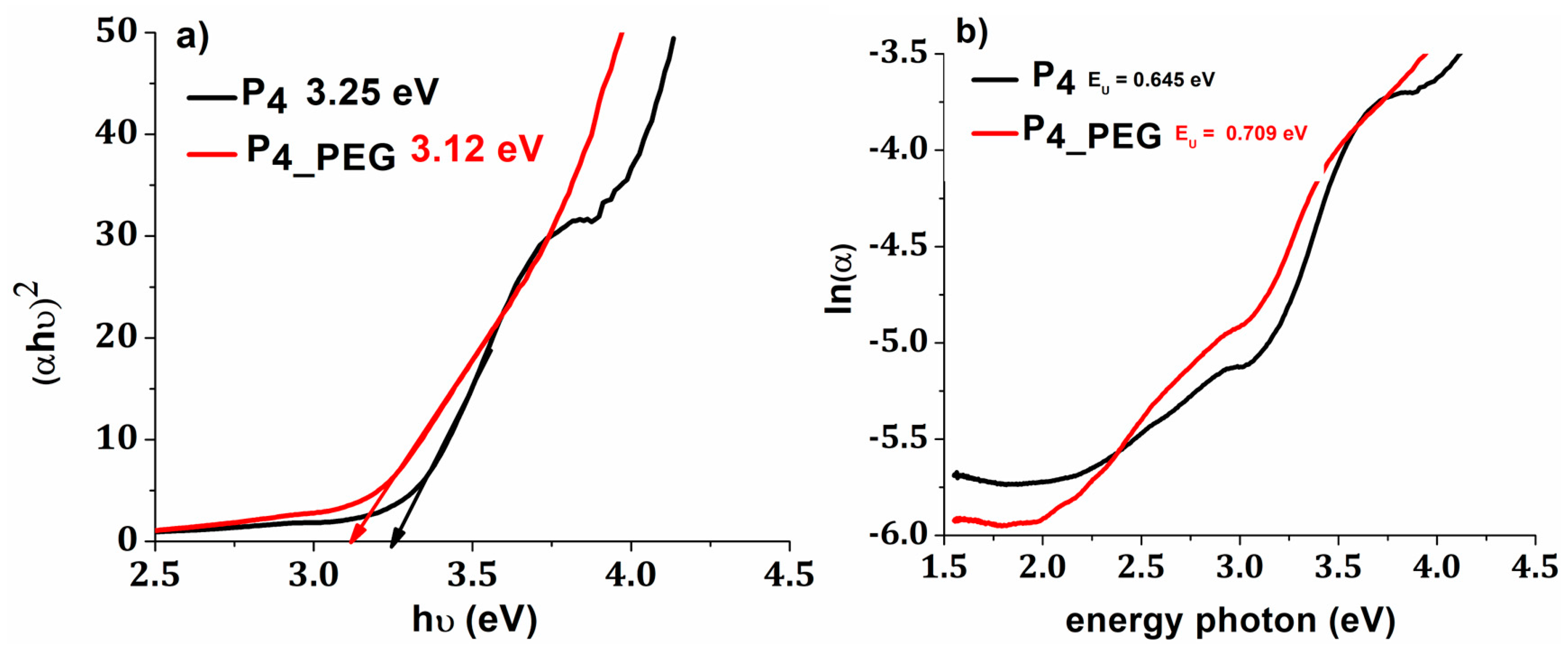
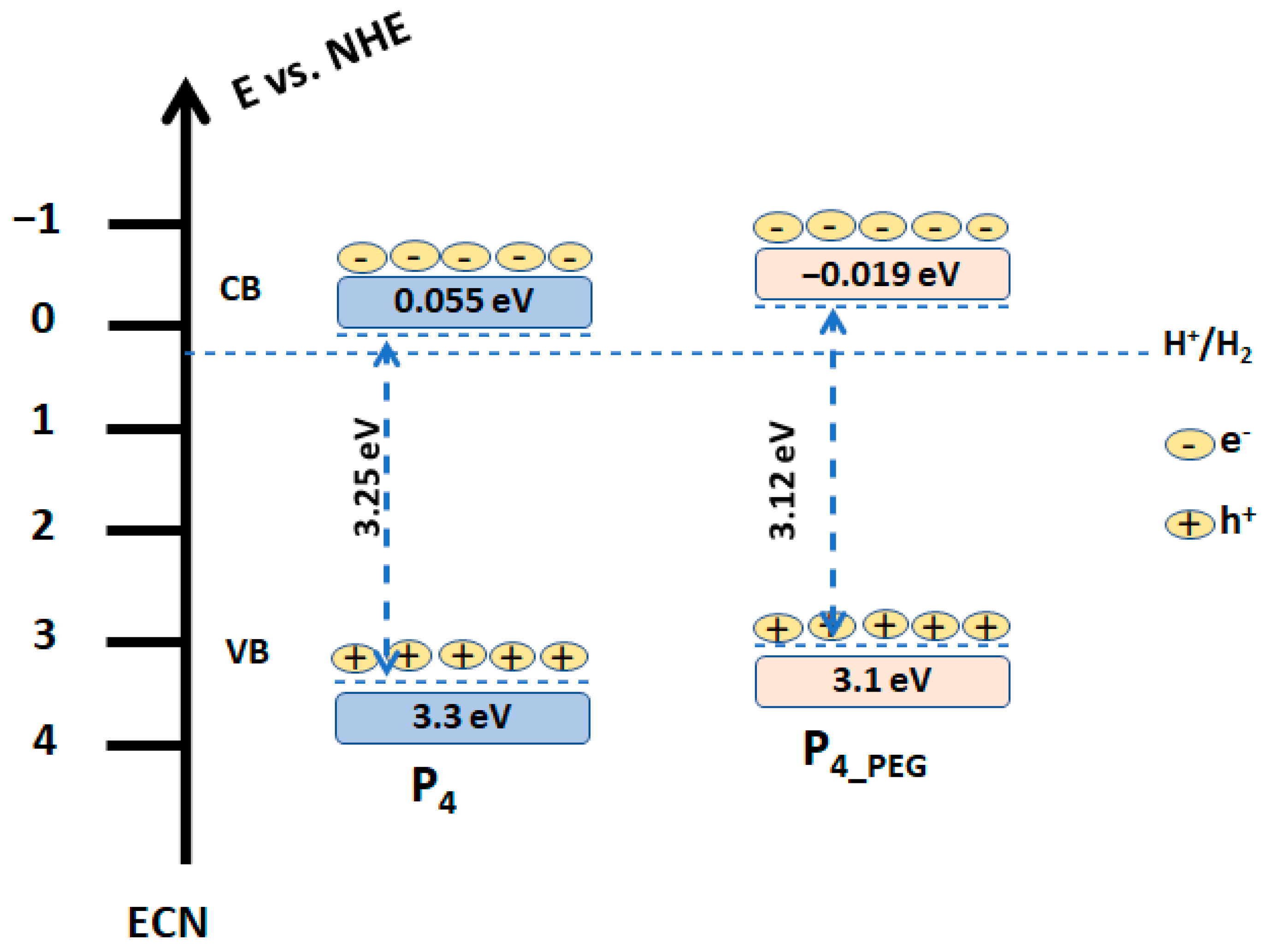
3.2.3. Optical Properties—Bandgap and Urbach Energies

Using Tauc’s equation (Equation (1)) and based on UV–VIS data, the band gap energy was determined.
The band gap (Eg) values for P4 were reduced from 3.25 eV to 3.12 eV for P4_PEG, indicating that the films are more conductive (Figure 11). In addition, for thin films made with a dispersant, the Urbach energy increased from 0.645 eV to 0.709 eV, with these values correlating with the increased surface free energy (Table 4). More structural defects, as shown by the Urbach energy value, can be induced by the delocalization of molecular orbitals caused by the simple breakdown of long interweaving PEG molecule chains, resulting in greater absorption at longer wavelengths and a decrease in band gap value [53,61].
The structure diagrams for the obtained films based on the measured M–S flat band potential and band gap from the UV–VIS data are shown in Figure 12. Based on the measured CB and Eg, the valence band (VB) energy of the films deposited on the FTO was computed.
As can be seen, P4 VB is 3.3 eV, while P4_PEG VB is 3.1 eV. When compared to P4 and P4_PEG, the VB is reduced by 0.2 eV. This suggested that the presence of PEG in solution 2 generates electrons on the surface of the film coated on the FTO substrate and improves conductivity, due to the well-controlled grain of the TiO2 (as depicted in Figure 5b), with greater crystallinity, as observed in the XRD data (Figure 6).
Based on these findings, the P4_PEG/FTO electrode can be employed in a variety of applications, including smart windows and photocatalysts for solar cells or water splitting, where pseudo-capacitive behavior is desired.

4. Conclusions and Perspectives

The surface characteristics of the TiO2 film deposited on the FTO substrate are enhanced by the incorporation of PEG into the sol–gel precursor solution used for the dip-coated deposition process. This results in a TiO2 film with increased free energy, as well as a more compact structure and nanoparticles with a higher degree of crystallization. The optical and electrochemical properties are affected by these surface features. With a higher insertion/extraction rate of protons into the P4_PEG nanostructure, the band gap is decreased from 3.25 to 3.12 eV, and the Urbach energy increases from 646 to 709 meV. The charge-transfer resistance is decreased from 418 kΩ to 23.4 kΩ, and the flat band potential is decreased from 0.44 V to −0.019 V, indicating improved catalytic properties of the final TiO2 film. These features make P4_PEG film a competitive option for technical uses such as smart windows, solar cells, photocatalysts and gas sensors.
Our long-term goal is to produce a pseudo-capacitive electrochromic electrode using this developed P4_PEG film as a template, which will be employed in the production of smart windows.

Author Contributions

Conceptualization, V.M.M.; data curation, V.M.M. and A.B.S.; formal analysis, V.M.M., R.T., E.V., A.B.S. and R.I.; investigation, V.M.M., R.T., E.V., A.B.S. and R.I.; methodology, V.M.M.; resources, V.M.M., R.T., E.V. and A.B.S.; writing—original draft, V.M.M. and R.I.; writing—review and editing, V.M.M.; All authors have read and agreed to the published version of the manuscript.

Funding

This work was supported by a grant from the Ministry of Research, Innovation and Digitization, CNCS—UEFISCDI, project number PN-III-P1-1.1-TE-2021-0417, within PNCDI III.

Institutional Review Board Statement

Not applicable.

Informed Consent Statement

Not applicable.

Data Availability Statement

The raw/processed data generated in this work are available upon request from the corresponding author.

Conflicts of Interest

The authors declare that they do not have any known competing financial interests or personal connections that could appear to have influenced the work presented in this study.

References

  1. Kumar, S.G.; Rao, K.S.R.K. Polymorphic phase transition among the titania crystal structures using a solution-based approach: From precursor chemistry to nucleation process. Nanoscale 2014, 6, 11574–11632. [Google Scholar] [CrossRef] [PubMed]
  2. Kumar, S.G.; Devi, L.G. Review on modified TiO2 photocatalysis under UV/visible light: Selected results and related mechanisms on interfacial charge carrier transfer dynamics. J. Phys. Chem. A 2011, 115, 13211–13241. [Google Scholar] [CrossRef] [PubMed]
  3. Tanveer, M.; Habib, A.; Khan, M. Infiltration of Polymer through the Pores of Electrospun Nanofibers and Performance of TiO2 Nanofibers/P3HT Photovoltaic Devices. Curr. Nanosci. 2013, 9, 351–356. [Google Scholar] [CrossRef]
  4. Hashimoto, K.; Irie, H.; Fujishima, A. TiO2 Photocatalysis: A Historical Overview and Future Prospects. Jpn. J. Appl. Phys. 2005, 44, 8269. [Google Scholar] [CrossRef]
  5. Mîndroiu, M.; Popescu, M. Fabrication of Ag/TiO2 nanotube array as active electrocatalyst for the hydrogen evolution reaction. Dig. J. Nanomater. Biostruct. 2022, 17, 999–1010. [Google Scholar] [CrossRef]
  6. Song, H.; Qiu, X.; Li, F. Effect of heat treatment on the performance of TiO2-Pt/CNT catalysts for methanol electro-oxidation. Electrochim. Acta 2008, 53, 3708–3713. [Google Scholar] [CrossRef]
  7. Ye, M.; Xin, X.; Lin, C.; Lin, Z. High Efficiency Dye-Sensitized Solar Cells Based on Hierarchically Structured Nanotubes. Nano Lett. 2011, 11, 3214–3220. [Google Scholar] [CrossRef]
  8. Huluba, R.; Pirvu, C.; Nicolescu, C.M.; Gheorghe, M.; Mindroiu, M. Counter electrode based on PEDOT: PSS-TiO2 NTs films for dye-sensitized solar cells. Mater. Plast. 2016, 53, 130–134. [Google Scholar]
  9. Dhandayuthapani, T.; Sivakumar, R.; Ilangovan, R.; Gopalakrishnan, C.; Sanjeeviraja, C.; Sivanantharaja, A.; Hari Krishna, R. Efficient electrochromic performance of anatase TiO2 thin films prepared by nebulized spray deposition method. J. Solid State Electrochem. 2018, 22, 1825–1838. [Google Scholar] [CrossRef]
  10. Fretwell, R.; Douglas, P. An Active, Robust and Transparent Nanocrystalline Anatase TiO2 Thin Film—Preparation, Characterisation and the Kinetics of Photodegradation of Model Pollutants. J. Photochem. Photobiol. A Chem. 2001, 143, 229–240. [Google Scholar] [CrossRef]
  11. Mîndroiu, M.; Pirvu, C.; Ion, R.; Demetrescu, I. Comparing performance of nanoarchitectures fabricated by Ti6Al7Nb anodizing in two kinds of electrolytes. Electrochim. Acta 2010, 56, 193–202. [Google Scholar] [CrossRef]
  12. Catauro, M.; Tranquillo, E.; Dal Poggetto, G.; Pasquali, M.; Dell’Era, A.; Vecchio Ciprioti, S. Influence of the Heat Treatment on the Particles Size and on the Crystalline Phase of TiO2 Synthesized by the Sol-Gel Method. Materials 2018, 11, 2364. [Google Scholar] [CrossRef] [PubMed]
  13. Zayim, E.O. Effect of calcination and pH value on the structural and optical properties of titanium oxide thin films. J. Mater. Sci. 2005, 40, 1345–1352. [Google Scholar] [CrossRef]
  14. Zhang, Q.; Gao, L.; Guo, J. Effect of hydrolysis conditions on morphology and crystallization of nanosized TiO2 powder. J. Eur. Ceram. Soc. 2000, 20, 2153–2158. [Google Scholar] [CrossRef]
  15. Wang, J.; Li, S.; Yan, W.; Tse, S.; Yao, Q. Synthesis of TiO2 nanoparticles by premixed stagnation swirl flames. Proc. Combust. Inst. 2011, 33, 1925–1932. [Google Scholar] [CrossRef]
  16. Ingrosso, C.; Bianco, G.V.; Pifferi, V.; Guffanti, P.; Petronella, F.; Comparelli, R.; Agostiano, A.; Striccoli, M.; Palchetti, I.; Falciola, L.; et al. TiO2 Nanocrystals Decorated CVD Graphene Based Hybrid for UV-Light Active Photoanodes. Procedia Eng. 2016, 168, 396–402. [Google Scholar] [CrossRef]
  17. Sung, Y.-M. Deposition of TiO2 Blocking Layers of Photovoltaic Cell Using RF Magnetron Sputtering Technology. Energy Procedia 2013, 34, 582–588. [Google Scholar] [CrossRef]
  18. Zeribi, F.; Attaf, A.; Derbali, A.; Saidi, H.; Benmebrouk, L.; Aida, M.S.; Dahnoun, M.; Nouadji, R.; Ezzaouia, H. Dependence of the Physical Properties of Titanium Dioxide (TiO2) Thin Films Grown by Sol-Gel (Spin-Coating) Process on Thickness. ECS J. Solid State Sci. Technol. 2022, 11, 023003. [Google Scholar] [CrossRef]
  19. Grilli, R.; Di Camillo, D.; Lozzi, L.; Horovitz, I.; Mamane, H.; Avisar, D.; Baker, M.A. Surface characterisation and photocatalytic performance of N-doped TiO2 thin films deposited onto 200 nm pore size alumina membranes by sol–gel methods. Mater. Chem. Phys. 2015, 159, 25–37. [Google Scholar] [CrossRef]
  20. Barati, N.; Sani, M.A.F.; Ghasemi, H.; Sadeghian, Z.; Mirhoseini, S.M.M. Preparation of uniform TiO2 nanostructure film on 316L stainless steel by sol–gel dip coating. Appl. Surf. Sci. 2009, 255, 8328–8333. [Google Scholar] [CrossRef]
  21. Zainal, Z.; Lee, C.Y. Properties and Photoelectrocatalytic Behaviour of Sol-Gel Derived TiO2 Thin Films. J. Sol-Gel Sci. Technol. 2006, 37, 19–25. [Google Scholar] [CrossRef]
  22. Che Halin, D.S.; Abdul Razak, K.; Sukeri, N.; Azani, A.; Abdullah, M.M.A.B.; Mohd Salleh, M.A.A.; Mahmed, N.; Ramli, M.; Azhari, A.; Chobpattana, V. The Effect of Polyethylene Glycol (PEG) on TiO2 Thin Films via Sol-Gel Method. IOP Conf. Ser. Mater. Sci. Eng. 2020, 743, 012007. [Google Scholar] [CrossRef]
  23. Wang, X.; Wu, G.; Zhou, B.; Shen, J. Optical Constants of Crystallized TiO2 Coatings Prepared by Sol-Gel Process. Materials 2013, 6, 2819–2830. [Google Scholar] [CrossRef] [PubMed]
  24. Wang, X.; Wu, G.; Zhou, B.; Shen, J. Thermal Annealing Effect on Optical Properties of Binary TiO2-SiO2 Sol-Gel Coatings. Materials 2013, 6, 76–84. [Google Scholar] [CrossRef] [PubMed]
  25. Jahromi, H.S.; Taghdisian, H.; Afshar, S.; Tasharrofi, S. Effects of pH and polyethylene glycol on surface morphology of TiO2 thin film. Surf. Coat. Technol. 2009, 203, 1991–1996. [Google Scholar] [CrossRef]
  26. Phattepur, H.; Siddaiah, G.; Ganganagappa, N. Synthesis and Characterisation of Mesoporous TiO2 Nanoparticles by Novel Surfactant Assisted Sol-gel Method for the Degradation of Organic Compounds. Period. Polytech. Chem. Eng. 2018, 63, 1–11. [Google Scholar] [CrossRef]
  27. Wang, H.-X.; Li, X.-X.; Tang, L. Effects of surfactants on the morphology and properties of TiO2. Appl. Phys. A 2020, 126, 448. [Google Scholar] [CrossRef]
  28. Lv, H.; Li, N.; Zhang, H.; Tian, Y.; Zhang, H.; Zhang, X.; Qu, H.; Liu, C.; Jia, C.; Zhao, J.; et al. Transferable TiO2 nanotubes membranes formed via anodization and their application in transparent electrochromism. Sol. Energy Mater. Sol. Cells 2016, 150, 57–64. [Google Scholar] [CrossRef]
  29. León, A.; Reuquen, P.; Garín, C.; Segura, R.; Vargas, P.; Zapata, P.; Orihuela, P.A. FTIR and Raman Characterization of TiO2 Nanoparticles Coated with Polyethylene Glycol as Carrier for 2-Methoxyestradiol. Appl. Sci. 2017, 7, 49. [Google Scholar] [CrossRef]
  30. Tsotetsi, D.; Dhlamini, M.; Mbule, P. Sol-gel derived mesoporous TiO2: Effects of non-ionic co-polymers on the pore size, morphology, specific surface area and optical properties analysis. Results Mater. 2022, 14, 100266. [Google Scholar] [CrossRef]
  31. Lungu, J.; Stefan, N.; Prodan, G.; Georgescu, A.; Mandes, A.; Ciupina, V.; Mihailescu, I.; Girtu, M. Characterization of spin-coated TiO2 buffer layers for dye-sensitized solar cells. Dig. J. Nanomater. Biostruct. 2015, 10, 967–976. [Google Scholar]
  32. Alhomoudi, I.; Thakur, J.; Naik, R.; Auner, G.; Newaz, G. Anatase TiO2 films based CO gas sensor: Film thickness, substrate and temperature effects. Appl. Surf. Sci. 2007, 253, 8607–8614. [Google Scholar] [CrossRef]
  33. Khan, M.I.; Imran, S.; Shahnawaz; Saleem, M.; Ur Rehman, S. Annealing effect on the structural, morphological and electrical properties of TiO2/ZnO bilayer thin films. Results Phys. 2018, 8, 249–252. [Google Scholar] [CrossRef]
  34. Ben Miled, I.; Jlassi, M.; Sta, I.; Dhaouadi, M.; Hajji, M.; Mousdis, G.A.; Kompitsas, M.G.; Ezzaouia, H. Influence of In-doping on microstructure, optical and electrical properties of sol–gel derived CdO thin films. J. Mater. Sci. Mater. Electron. 2018, 29, 11286–11295. [Google Scholar] [CrossRef]
  35. Dundar, I.; Mere, A.; Mikli, V.; Krunks, M.; Oja Acik, I. Thickness Effect on Photocatalytic Activity of TiO2 Thin Films Fabricated by Ultrasonic Spray Pyrolysis. Catalysts 2020, 10, 1058. [Google Scholar] [CrossRef]
  36. Mechiakh, R.; Ben Sedrine, N.; Chtourou, R. Sol–gel synthesis, characterization and optical properties of mercury-doped TiO2 thin films deposited on ITO glass substrates. Appl. Surf. Sci. 2011, 257, 9103–9109. [Google Scholar] [CrossRef]
  37. Witit-anun, N.; Rakkwamsuk, P.; Limsuwan, P. Characterization of Anatase and Rutile TiO2 Thin Films Deposited by Two Cathodes Sputtering System. Adv. Mater. Res. 2008, 55–57, 469–472. [Google Scholar] [CrossRef]
  38. Derbali, A.; Attaf, A.; Saidi, H.; Benamra, H.; Nouadji, M.; Aida, M.S.; Attaf, N.; Ezzaouia, H. Investigation of structural, optical and electrical properties of ZnS thin films prepared by ultrasonic spray technique for photovoltaic applications. Optik 2018, 154, 286–293. [Google Scholar] [CrossRef]
  39. Ghribi, F.; El Mir, L.; Omri, K.; Djessas, K. Sputtered ZnS thin film from nanoparticles synthesized by hydrothermal route. Optik 2016, 127, 3688–3692. [Google Scholar] [CrossRef]
  40. Attaf, A.; Derbali, A.; Saidi, H.; Benamra, H.; Aida, M.S.; Attaf, N.; Ezzaouia, H.; Derbali, L. Physical properties of Pb doped ZnS thin films prepared by ultrasonic spray technique. Phys. Lett. A 2020, 384, 126199. [Google Scholar] [CrossRef]
  41. Sreemany, M.; Sen, S. A simple spectrophotometric method for determination of the optical constants and band gap energy of multiple layer TiO2 thin films. Mater. Chem. Phys. 2004, 83, 169–177. [Google Scholar] [CrossRef]
  42. Islam, S.Z.; Reed, A.; Kim, D.Y.; Rankin, S.E. N2/Ar plasma induced doping of ordered mesoporous TiO2 thin films for visible light active photocatalysis. Microporous Mesoporous Mater. 2016, 220, 120–128. [Google Scholar] [CrossRef]
  43. Tomasz, T.; Matysiak, W.; Kosmalska, D.; Lubos, A. Influence of calcination temperature on optical and structural properties of TiO2 thin films prepared by means of sol-gel and spin coating. Bull. Pol. Acad. Sci. Tech. Sci. 2018, 66, 151–156. [Google Scholar]
  44. Zanello, P.; Connelly, N.G. Inorganic Electrochemistry; The Royal Society of Chemistry: London, UK, 2003. [Google Scholar]
  45. Hu, X.; Zhu, Q.; Wang, X.; Kawazoe, N.; Yang, Y. Nonmetal–metal–semiconductor-promoted P/Ag/Ag2O/Ag3PO4/TiO2 photocatalyst with superior photocatalytic activity and stability. J. Mater. Chem. A 2015, 3, 17858–17865. [Google Scholar] [CrossRef]
  46. Mao, H.; Fei, Z.; Bian, C.; Yu, L.; Chen, S.; Qian, Y. Facile synthesis of high-performance photocatalysts based on Ag/TiO2 composites. Ceram. Int. 2019, 45, 12586–12589. [Google Scholar] [CrossRef]
  47. Haider, A.J.; Al-Anbari, R.H.; Kadhim, G.R.; Salame, C.T. Exploring potential Environmental applications of TiO2 Nanoparticles. Energy Procedia 2017, 119, 332–345. [Google Scholar] [CrossRef]
  48. Wu, W.-J.; He, W.-L.; Yu, H.-Y.; Huang, H.-X.; Chen, M.; Qian, D.-J. Synthesis and photophysical properties of pyrene-functionalized nano-SiO2 hybrids in solutions and doped-PMMA thin films. Mater. Chem. Phys. 2017, 186, 179–187. [Google Scholar] [CrossRef]
  49. Rahim, S.; Sasani Ghamsari, M.; Radiman, S. Surface modification of titanium oxide nanocrystals with PEG. Sci. Iran. 2012, 19, 948–953. [Google Scholar] [CrossRef]
  50. Li, R.; Wu, Y.; Bai, Z.; Guo, J.; Chen, X. Effect of molecular weight of polyethylene glycol on crystallization behaviors, thermal properties and tensile performance of polylactic acid stereocomplexes. RSC Adv. 2020, 10, 42120–42127. [Google Scholar] [CrossRef]
  51. Praveen, P.; Viruthagiri, G.; Mugundan, S.; Shanmugam, N. Structural, optical and morphological analyses of pristine titanium di-oxide nanoparticles—Synthesized via sol–gel route. Spectrochim. Acta Part A Mol. Biomol. Spectrosc. 2014, 117, 622–629. [Google Scholar] [CrossRef]
  52. Hu, S.; Wang, A.; Li, X.; Holger, L. Hydrothermal Synthesis of Well-dispersed Ultrafine N-Doped TiO2 Nanoparticles with Enhanced Photocatalytic Activity under Visible Light. J. Phys. Chem. Solids 2010, 71, 156–162. [Google Scholar] [CrossRef]
  53. Mahadik, S.A.; Yadav, H.M.; Mahadik, S.S. Surface properties of chlorophyll-a sensitized TiO2 nanorods for dye-sensitized solar cells applications. Colloid Interface Sci. Commun. 2022, 46, 100558. [Google Scholar] [CrossRef]
  54. Peng, Z.; Ni, J. Surface properties and bioactivity of TiO2 nanotube array prepared by two-step anodic oxidation for biomedical applications. R. Soc. Open Sci. 2019, 6, 181948. [Google Scholar] [CrossRef]
  55. Song, Y.; Gao, Z.D.; Wang, J.; Xia, X.; Lynch, R.P. Multistage Coloring Electrochromic Device Based on TiO2 Nanotube Arrays Modified with WO3 Nanoparticles. Adv. Funct. Mater. 2011, 21, 1941–1946. [Google Scholar] [CrossRef]
  56. Wu, F.; Chen, J.; Li, L.; Zhao, T.; Liu, Z.; Chen, R. Polyethylene-Glycol-Doped Polypyrrole Increases the Rate Performance of the Cathode in Lithium–Sulfur Batteries. ChemSusChem 2013, 6, 1438–1444. [Google Scholar] [CrossRef]
  57. Mindroiu, M.; Ion, R.; Pirvu, C.; Cimpean, A. Surfactant-dependent macrophage response to polypyrrole-based coatings electrodeposited on Ti6Al7Nb alloy. Mater. Sci. Eng. C 2013, 33, 3353–3361. [Google Scholar] [CrossRef] [PubMed]
  58. Ungureanu, C.; Barbulescu, L.; Dumitriu, C.; Manole, C.; Pirvu, C. Titanium industrial residues surface modification towards its reuse as antimicrobial surfaces. Environ. Sci. Pollut. Res. 2021, 28, 38224–38237. [Google Scholar] [CrossRef] [PubMed]
  59. Gelderman, K.; Lee, L.; Donne, S. Flat-Band Potential of a Semiconductor: Using the Mott Schottky Equation. J. Chem. Educ. 2007, 84, 685. [Google Scholar] [CrossRef]
  60. Sang, L.; Tan, H.; Zhang, X.; Wu, Y.; Ma, C.; Burda, C. Effect of Quantum Dot Deposition on the Interfacial Flatband Potential, Depletion Layer in TiO2 Nanotube Electrodes, and Resulting H2 Generation Rates. J. Phys. Chem. C 2012, 116, 18633–18640. [Google Scholar] [CrossRef]
  61. Vidyasagar, C.C.; Arthoba Naik, Y. Surfactant (PEG 400) effects on crystallinity of ZnO nanoparticles. Arab. J. Chem. 2016, 9, 507–510. [Google Scholar] [CrossRef]
Figure 1. A simplified schematic of the procedure followed to obtain the TiO2 thin films on FTO substrate by dip-coating method.
Materials 16 03147 g001
Figure 2. AFM images of TiO2 films obtained from solution 1 by (a) two dip-coating cycles, (b) four dip-coating cycles, (c) six dip-coating cycles, (d) eight dip-coating cycles, and (e) FTO substrate.
Materials 16 03147 g002
Figure 3. (a) Optical transmittance; (b) plot of (αhν)2 versus hν; and (c) ln(α) versus photon energy plot for TiO2 thin films deposited on an FTO substrate from solution 1, using different number of dip-coating layers.
Materials 16 03147 g003
Figure 4. Cycle Voltammetry for (a) P2; (b) P4; (c) P6; (d) P8 between −0.6 V and 0.2 V vs. Ag/AgCl at 50 mV s−1, 100 cycles, in 0.5 M H2SO4 aqueous solution.
Materials 16 03147 g004
Figure 5. SEM images of (a) P4 and (b) P4_PEG. EDAX analysis of (c) P4 and (d) P4_PEG.
Materials 16 03147 g005
Figure 6. The X-ray diffraction (XRD) patterns of P4 and P4_PEG thin films dip-coated on FTO substrate.
Materials 16 03147 g006
Figure 7. FTIR spectra of TiO2 thin films obtained from sol–gel solution with/without PEG.
Materials 16 03147 g007
Figure 8. The cyclic voltammograms of (a) P4 and (b) P4_PEG films on FTO at various scan rates, with an insert displaying the plot of oxidation peak current densities vs. square root of potential scan rate.
Materials 16 03147 g008
Figure 9. Nyquist plots for P4 and P4_PEG films.
Materials 16 03147 g009
Figure 10. Mott–Schotky (M-S) plots for (a) P4 and (b) P4_PEG films.
Materials 16 03147 g010
Figure 11. (a) plot of (αhν)2 versus hν; and (b) plot of ln(α) versus photon energy.
Materials 16 03147 g011
Figure 12. Schematic diagram of the band gap of the P4 and P4_PEG.
Materials 16 03147 g012
Table 1. The thickness and roughness of TiO2 films.
Number of LayersFilm Thickness,
µm
Roughness Average (Ra),
µm
20.674 ± 0.0570.667 ± 0.074
41.346 ± 0.0950.432 ± 0.065
61.881 ± 0.0510.412 ± 0.038
81.945 ± 0.0550.259 ± 0.045
FTO-0.004 ± 0.002
Table 2. Band gap and Urbach energies for TiO2 thin films deposited on FTO substrate using sol–gel dip-coating at varying cycle numbers.
Number of LayersBand Gap Energy, Eg
(eV)
Urbach Energy, Eu
(eV)
23.52 ± 0.018
3.25 ± 0.013
3.28 ± 0.017
3.26 ± 0.009
3.68 ± 0.018
0.3104 ± 0.005
0.6459 ± 0.012
0.6142 ± 0.011
0.61337 ± 0.013
0.2787 ± 0.013
4
6
8
FTO
Table 3. Crystallite sizes, strain, and dislocation density values of P4 and P4_PEG thin films from XRD results.
SamplesPeak (hkl)2-ThetaFWHM (β)D (nm) ε   ×   10 4 δ × 10 15 (m−2)
P4(101)26.500.384 22.14 3.75 2.04
P4_PEG(101)26.560.23636.09 2.43 0.76
Table 4. Surface energy of TiO2 film as a function of dispersants added in sol–gel solution.
SamplesContact Angle,
(°)
Surface Energy,
(mJ m2)
DI WaterEGDMSO
P426 ± 0.6717 ± 0.2429 ± 0.1467
P4_PEG16 ± 0.215 ± 0.843 ± 0.6071
Table 5. Electric parameters from fitting experimental EIS data.
SamplesElectric Parameters
Rs
(Ω cm2)
Rct
(Ω cm2)
CPE
−1 cm−2 sn)
n
P421.60418.0 × 10311.08 × 10−60.803
P4_PEG15.5023.4 × 1032.48 × 10−30.975
Disclaimer/Publisher’s Note: The statements, opinions and data contained in all publications are solely those of the individual author(s) and contributor(s) and not of MDPI and/or the editor(s). MDPI and/or the editor(s) disclaim responsibility for any injury to people or property resulting from any ideas, methods, instructions or products referred to in the content.

