
Strain-Balanced InAs/AlSb Type-II Superlattice Structures Growth on GaSb Substrate by Molecular Beam Epitaxy

 , , ,
, , ,
Abstract
1. Introduction
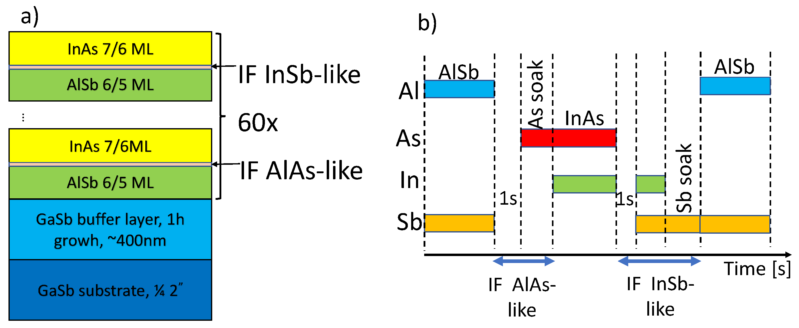
2. Experiment
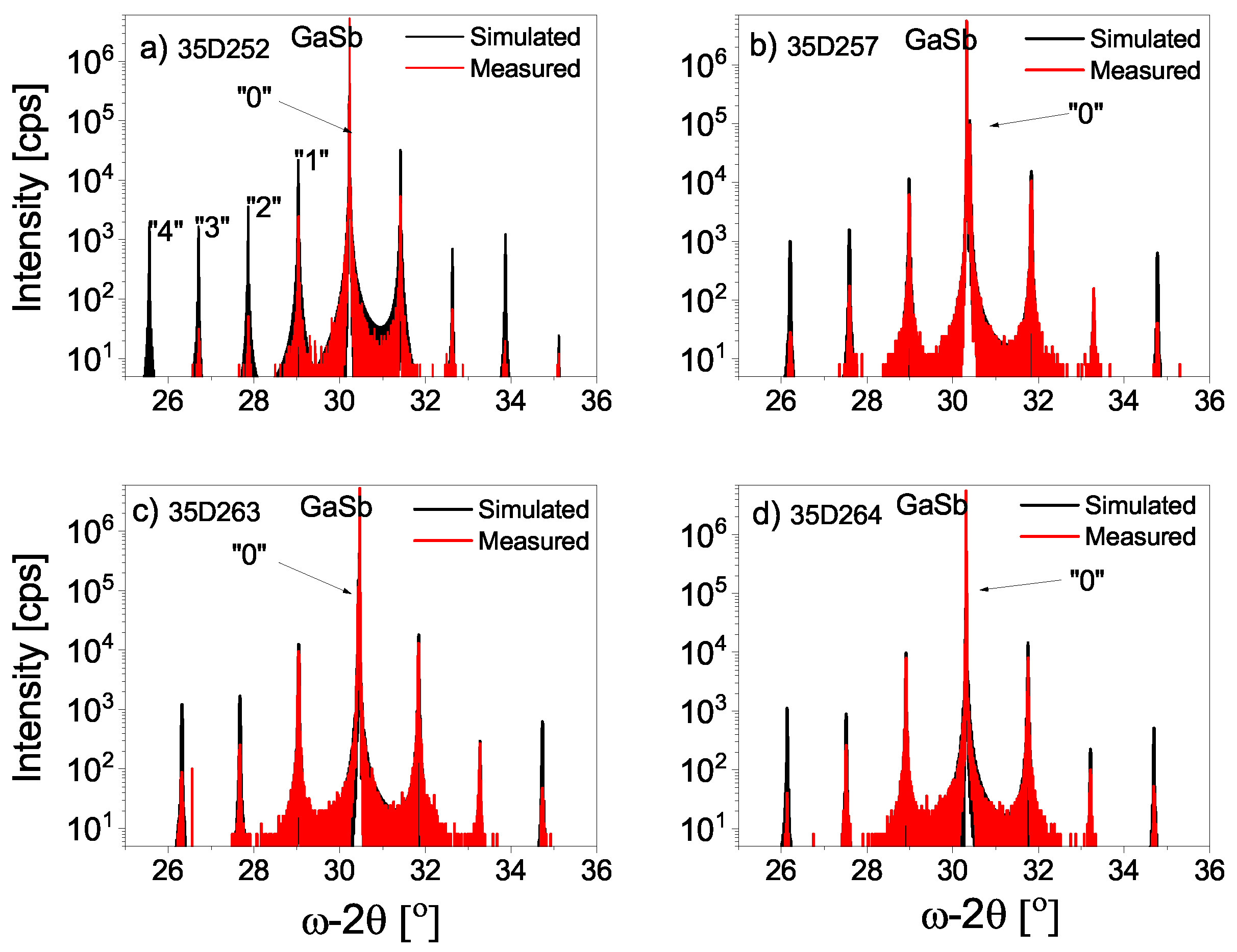
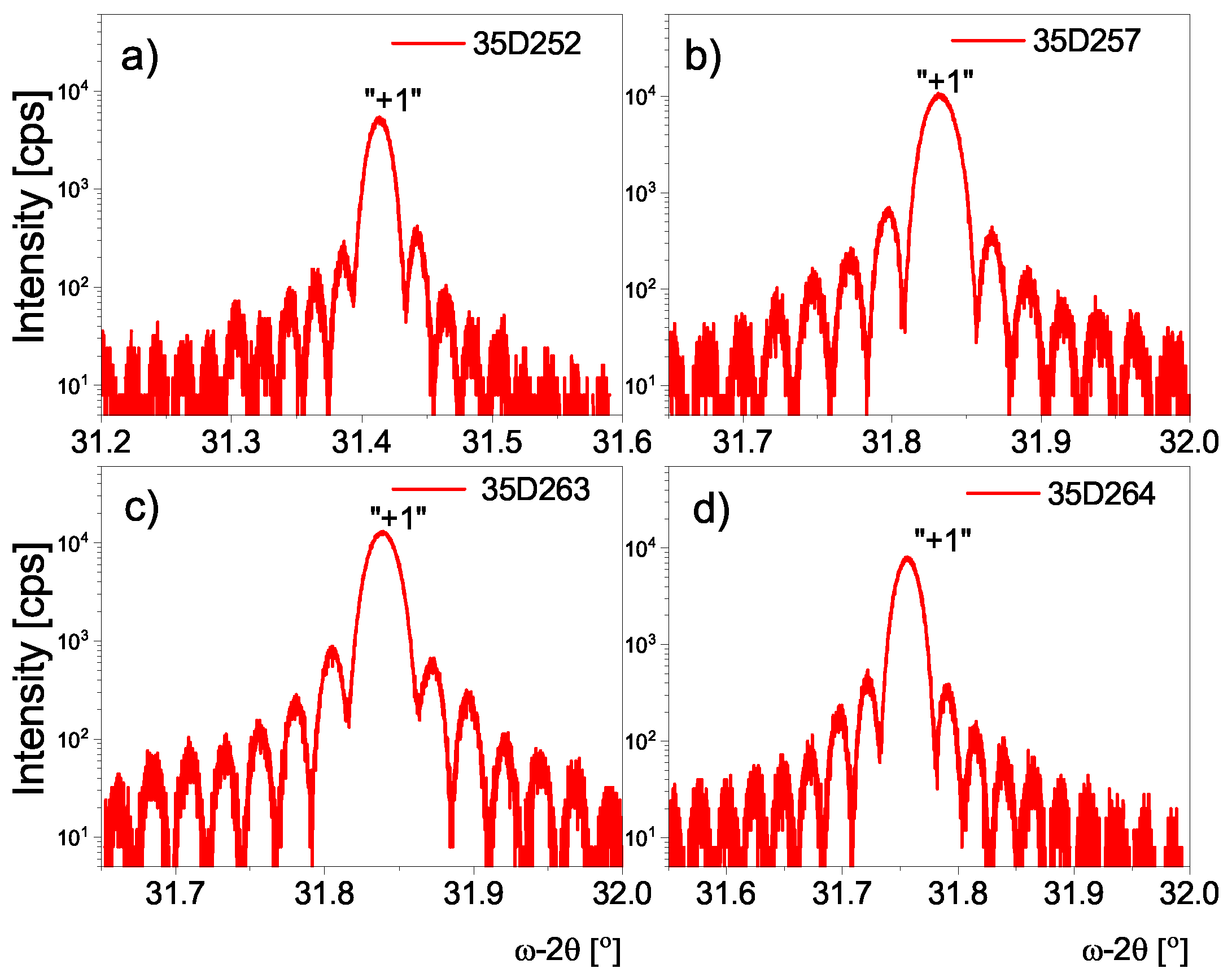
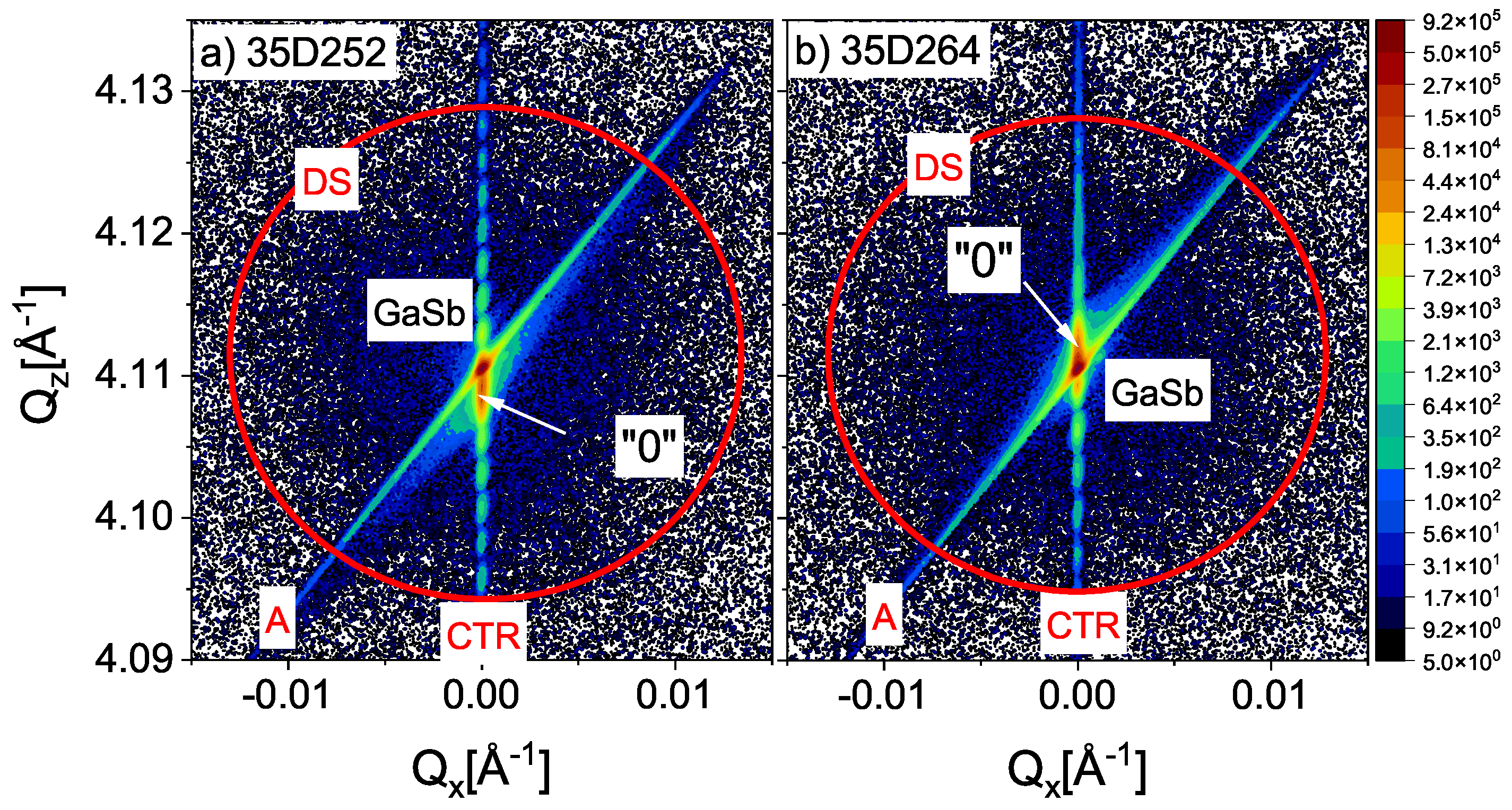
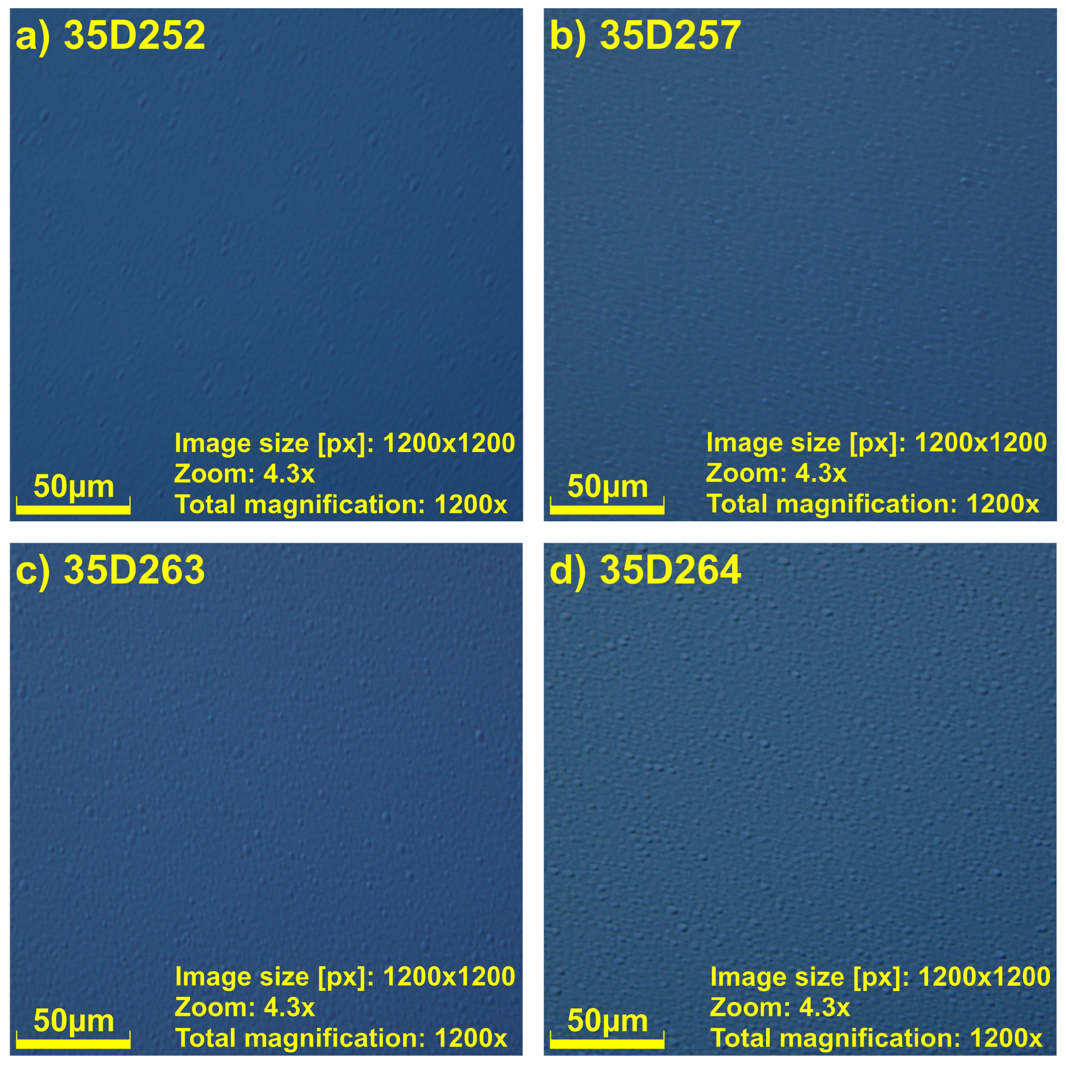
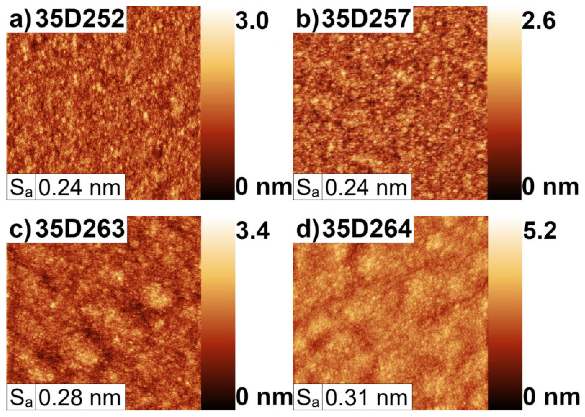
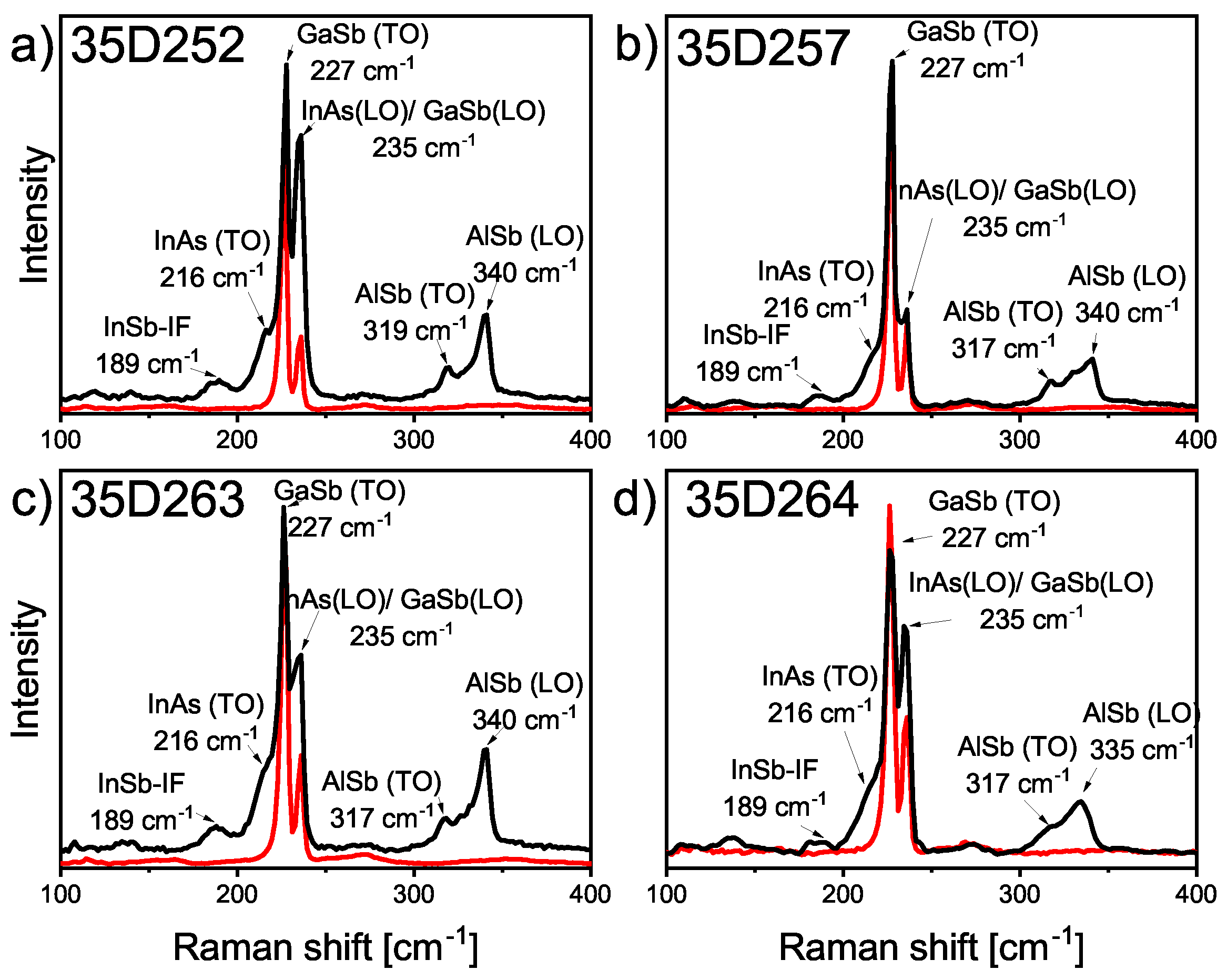
3. Results and Discussion
4. Summary
Author Contributions
Funding
Institutional Review Board Statement
Informed Consent Statement
Data Availability Statement
Conflicts of Interest
Sample Availability
Abbreviations
| MBE | Molecular Beam Epitaxy |
| T2SL | Type Two Superlattice |
| HRXRD | High Resolution X-Ray Diffraction |
| AFM | Atomic Force Microscopy |
References
- Nie, B.; Huang, J.; Zhao, C.; Huang, W.; Zhang, Y.; Cao, Y.; Ma, W. InAs/GaSb superlattice resonant tunneling diode photodetector with InAs/AlSb double barrier structure. Appl. Phys. Lett. 2019, 114, 053509. [Google Scholar] [CrossRef]
- Martyniuk, P.; Kopytko, M.; Rogalski, A. Barrier infrared detectors. Opto-Electron. Rev. 2014, 22, 127–146. [Google Scholar] [CrossRef]
- Gautam, N.; Myers, S.; Barve, A.V.; Klein, B.; Smith, E.P.; Rhiger, D.R.; Dawson, L.R.; Krishna, S. High operating temperature interband cascade midwave infrared detector based on type-II InAs/GaSb strained layer superlattice. Appl. Phys. Lett. 2012, 101, 021106. [Google Scholar] [CrossRef]
- Kroemer, H. The 6.1 A family (InAs, GaSb, AlSb) and its heterostructures: A selective review. Phys. E 2004, 20, 196–203. [Google Scholar] [CrossRef]
- Alshahrani, D.O.; Kesaria, M.; Anyebe, E.A.; Srivastava, V.; Huffaker, D.L. Emerging Type-II Superlattices of InAs/InAsSb and InAs/GaSb for Mid-Wavelength Infrared Photodetectors. Adv. Photonics Res. 2022, 3, 2100094. [Google Scholar] [CrossRef]
- Haugan, H.J.; Brown, G.J.; Grazulis, L. Effect of interfacial formation on the properties of very long wavelength infrared InAs/GaSb superlattices. J. Vac. Sci. Technol. B 2011, 29, 03C101. [Google Scholar]
- Jasik, A.; Sankowska, I.; Pierścińska, D.; Regiński, K.; Pierściński, K. Blueshift of bandgap energy and reduction of non-radiative defect density due to precise control of InAs-on-GaSb interface in type-II InAs/GaSb superlattice. J. Appl. Phys. 2011, 110, 123103. [Google Scholar] [CrossRef]
- Jasik, A.; Sankowska, I.; Regiński, K.; Machowska-Podsiadło, E.; Wawro, A.; Wzorek, M.; Kruszka, R.; Jakieła, R.; Kubacka-Traczyk, J.; Motyka, M.; et al. Crystal Growth: Theory, Mechanisms and Morphology; Nova Scicnce Publisheres, Inc.: New York, NY, USA, 2012; Volume 2, Chapter 9, pp. 293–326. [Google Scholar]
- Du, L.; Li, X.; Lou, W.; Sullivan, G.; Chang, K.; Kono, J.; Du, R.R. Evidence for a topological excitonic insulator in InAs/GaSb bilayers. Nat. Commun. 2017, 8, 1971. [Google Scholar] [CrossRef]
- Müller, R.; Haertelt, M.; Niemasz, J.; Schwarz, K.; Daumer, V.; Flores, Y.V.; Ostendorf, R.; Rehm, R. Thermoelectrically-cooled InAs/GaSb Type-II superlattice detectors as an alternative to HgCdTe in a real-time mid-infrared backscattering spectroscopy system. Micromachines 2020, 11, 1124. [Google Scholar] [CrossRef]
- Fang, S.; Hao, R.; Zhang, L.; Guo, J.; Liu, W. Simulation of the band structure of InAs/GaSb type II superlattices utilizing multiple energy band theories. Front. Phys. 2022, 10, 822800. [Google Scholar] [CrossRef]
- Zhang, Y.; Ma, W.; Cao, Y.; Huang, J.; Wei, Y.; Cui, K.; Shao, J. Long wavelength infrared InAs/GaSb superlattice photodetectors with InSb-like and mixed interfaces. IEEE J. Quantum Electron. 2011, 47, 1475. [Google Scholar] [CrossRef]
- Nicolai, J.; Warot-Fonrose, B.; Gatel, C.; Teissier, R.; Baranov, A.N.; Magen, C.; Ponchet, A. Formation of strained interfaces in AlSb/InAs multilayers grown by molecular beam epitaxy for quantum cascade lasers. J. Appl. Phys. 2015, 118, 035305. [Google Scholar] [CrossRef]
- Kubacka-Traczyk, J.; Sankowska, I.; Kaniewski, J. Interface Influence on Structural Properties of InAs/GaSb Type-II Superlattices. Opt. Appl. 2009, 39, 875–879. [Google Scholar]
- Tuttle, G.; Kroemer, H.; English, J.H. Effects of interface layer sequencing on the transport properties of InAs/AlSb quantum wells: Evidence for antisite donors at the InAs/AlSb interface. J. Appl. Phys. 1990, 67, 3032–3037. [Google Scholar] [CrossRef]
- Brar, B.; Ibbetson, J.; Kroemer, H.; English, J.H. Effects of the interface bonding type on the optical and structural properties of InAs-AlSb quantum wells. Appl. Phys. Lett. 1994, 64, 3392–3394. [Google Scholar] [CrossRef]
- Benyahia, D.; Kubiszyn, L.; Michalczewski, K.; Kębłowski, A.; Grodecki, K.; Martyniuk, P. Molecular beam epitaxy growth of InAs/AlSb superlattices on GaAs substrates. J. Cryst. Growth 2019, 522, 125–127. [Google Scholar] [CrossRef]
- Xu, Z.; Chen, J.; Wang, F.; Zhou, Y.; Jin, C.; He, L. Interface layer control and optimization of InAs/GaSb type-II superlattices grown by molecular beam epitaxy. J. Cryst. Growth 2014, 286, 220–225. [Google Scholar] [CrossRef]
- Mishra, P.; Pandey, R.K.; Kumari, S.; Pandey, A.; Dalal, S.; Sankarasubramanian, R.; Channagiri, S.; Jangir, S.K.; Raman, R.; Srinivasan, T.; et al. Interface engineered MBE grown InAs/GaSb based type-II superlattice heterostructures. J. Alloys Compd. 2021, 889, 161692. [Google Scholar] [CrossRef]
- Sankowsk, I.; Jasik, A.; Czuba, K.; Ratajczak, J.; Kozłowski, P.; Wzorek, M. A Study of Defects in InAs/GaSb Type-II Superlattices Using High-Resolution Reciprocal Space Mapping. Materials 2021, 14, 4940. [Google Scholar] [CrossRef]
- Xu, D.; Litvinchuk, A.P.; Wang, X.; Delaney, A.; Le, H.; Pei, S.S. Structure stability of short-period InAs/AlSb superlattices. J. Cryst. Growth 2003, 251, 547–550. [Google Scholar] [CrossRef]
- Zhang, Y.; Zhang, Y.; Guan, M.; Cui, L.; Li, Y.; Wang, B.; Zhu, Z.; Zeng, Y. Molecular beam epitaxial growth of AlSb/InAsSb heterostructures. Appl. Surf. Sci. 2014, 313, 479–483. [Google Scholar] [CrossRef]


| T2SL | InAs/AlSb | IF | IFAlAs | Δa/a |
|---|---|---|---|---|
| No. | (ML)/(ML) | (ML) | (ML) | × 10 |
| 35D252 | 7.1/6.0 | 0.75 | 0.42 | 3.2 |
| 35D257 | 6.0/5.0 | 0.47 | 0.43 | 21.8 |
| 35D263 | 6.0/5.1 | 0.67 | 0.35 | 8.9 |
| 35D264 | 5.8/5.3 | 0.50 | 0.35 | 0.8 |
Disclaimer/Publisher’s Note: The statements, opinions and data contained in all publications are solely those of the individual author(s) and contributor(s) and not of MDPI and/or the editor(s). MDPI and/or the editor(s) disclaim responsibility for any injury to people or property resulting from any ideas, methods, instructions or products referred to in the content. |
© 2023 by the authors. Licensee MDPI, Basel, Switzerland. This article is an open access article distributed under the terms and conditions of the Creative Commons Attribution (CC BY) license (https://creativecommons.org/licenses/by/4.0/).
Share and Cite
Marchewka, M.; Jarosz, D.; Ruszała, M.; Juś, A.; Krzemiński, P.; Płoch, D.; Maś, K.; Wojnarowska-Nowak, R. Strain-Balanced InAs/AlSb Type-II Superlattice Structures Growth on GaSb Substrate by Molecular Beam Epitaxy. Materials 2023, 16, 1968. https://doi.org/10.3390/ma16051968
Marchewka M, Jarosz D, Ruszała M, Juś A, Krzemiński P, Płoch D, Maś K, Wojnarowska-Nowak R. Strain-Balanced InAs/AlSb Type-II Superlattice Structures Growth on GaSb Substrate by Molecular Beam Epitaxy. Materials. 2023; 16(5):1968. https://doi.org/10.3390/ma16051968
Chicago/Turabian StyleMarchewka, Michał, Dawid Jarosz, Marta Ruszała, Anna Juś, Piotr Krzemiński, Dariusz Płoch, Kinga Maś, and Renata Wojnarowska-Nowak. 2023. "Strain-Balanced InAs/AlSb Type-II Superlattice Structures Growth on GaSb Substrate by Molecular Beam Epitaxy" Materials 16, no. 5: 1968. https://doi.org/10.3390/ma16051968
APA StyleMarchewka, M., Jarosz, D., Ruszała, M., Juś, A., Krzemiński, P., Płoch, D., Maś, K., & Wojnarowska-Nowak, R. (2023). Strain-Balanced InAs/AlSb Type-II Superlattice Structures Growth on GaSb Substrate by Molecular Beam Epitaxy. Materials, 16(5), 1968. https://doi.org/10.3390/ma16051968