Two-Level 3D Column-like Nanofilms with Hexagonally–Packed Tantalum Fabricated via Anodizing of Al/Nb and Al/Ta Layers—A Potential Nano-Optical Biosensor
Abstract
1. Introduction
| Oxide | µr | εr |
|---|---|---|
| NbO2 | 1.0000003 [34] | 10 [40] |
| Nb2O5 | 0.9999998 [33] | 32–45 [35,36] |
| TaO2 | 1.0000032 [34] | 27.5 [41] |
| Ta2O5 | 0.9999994 [33] | Ta2O5 (α), [33] Ta2O5 (β) εr = 24 [33] |
| WO2 | 1.0000029 [33] | 5–12 [42] |
| WO3 | 0.9999995 [33] | 300 [33] |
| HfO2 | 0.9999989 [33] | 16–19 [37] |
2. Materials and Methods
2.1. First-Level Column-like Anodic Niobia Nanofilm Preparation
2.2. Second-Level Column-like Anodic Tantala Nanofilm Preparation
2.3. Nanofilms Analysis
2.4. Data Processing and Optical Simulations
3. Results and Discussion
3.1. First-Level Anodic Niobia Nanofilm Morphology
3.2. Morphology and Structure of Sputter-Deposited Al/Ta Bilayer
3.3. Second-Level Anodic Tantala Nanofilm Morphology
3.4. Second-Level Morphology after Long Room Temperature Chemical Etching
3.5. Model of Film Growth during Anodizing and Reanodizing
3.6. Optical Simulation for Biosensor Applications
4. Conclusions
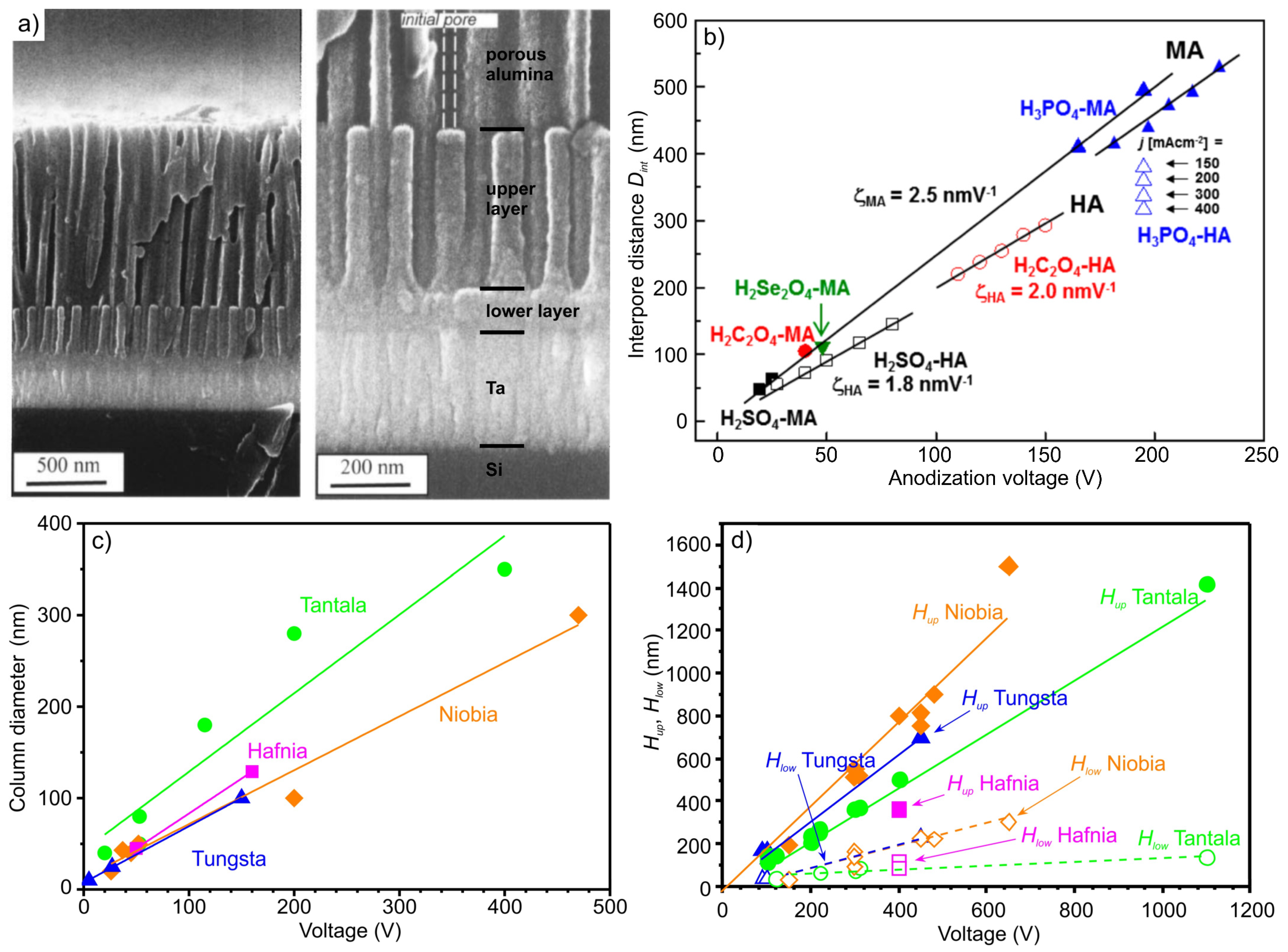
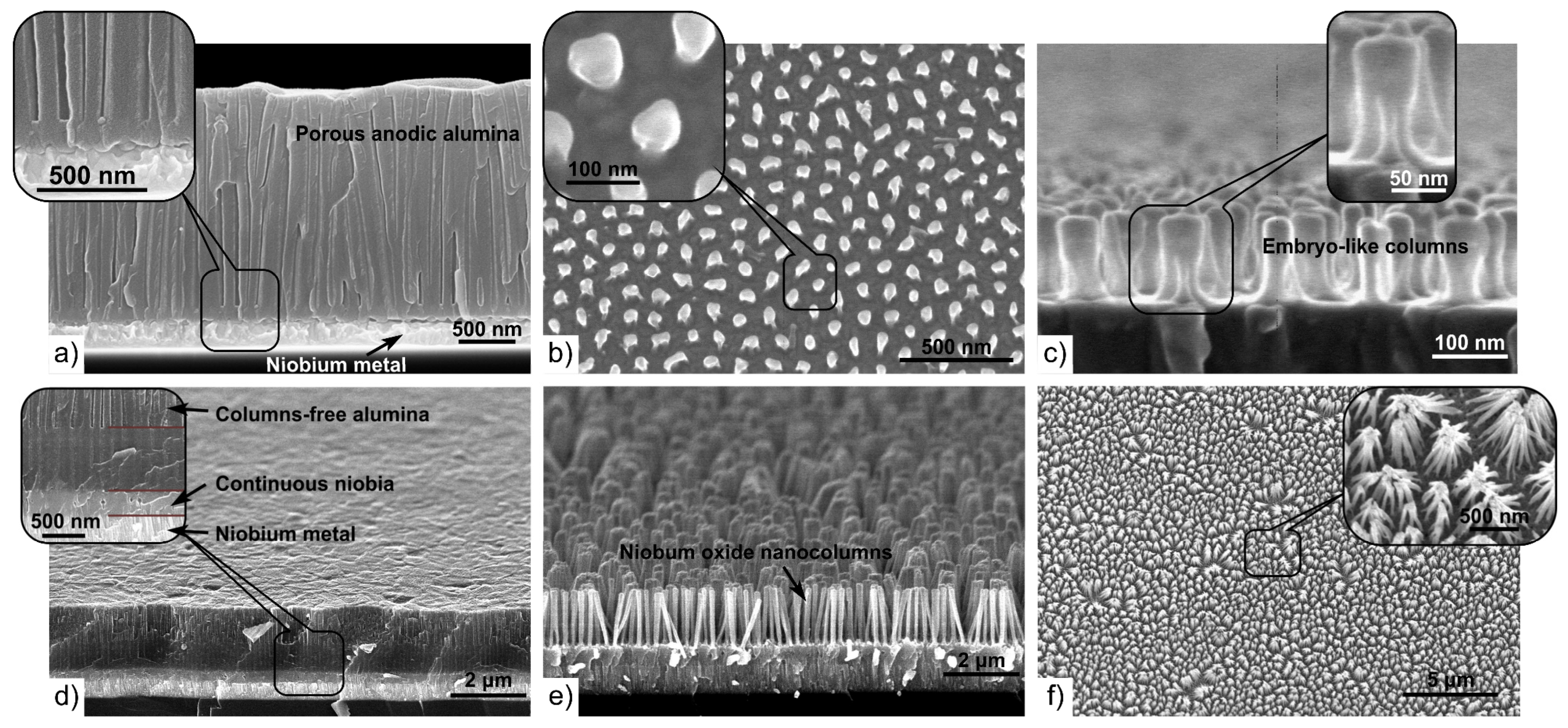
- A first-level column-like 3D nanofilm, in which an array of niobia nanocolumns (∼57 nm diameter and ∼130 nm distance) penetrate the pores of a ∼163-nm-thick anodic alumina film, emerging above the film at ∼281 nm, has been fabricated by anodizing Al/Nb layers coated on silicon. The columns have the same structure and thickness along the entire length, in contrast to the skittle-like columns formed at higher voltages.
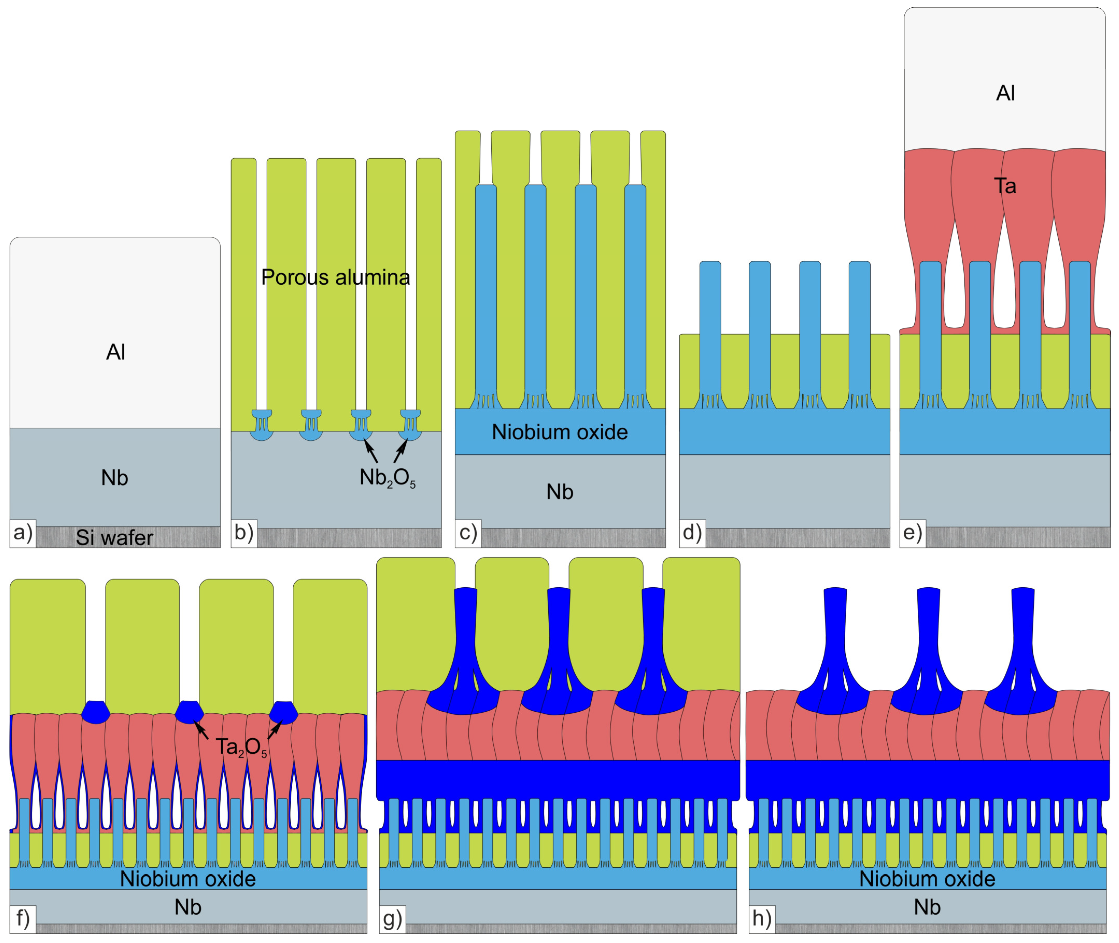
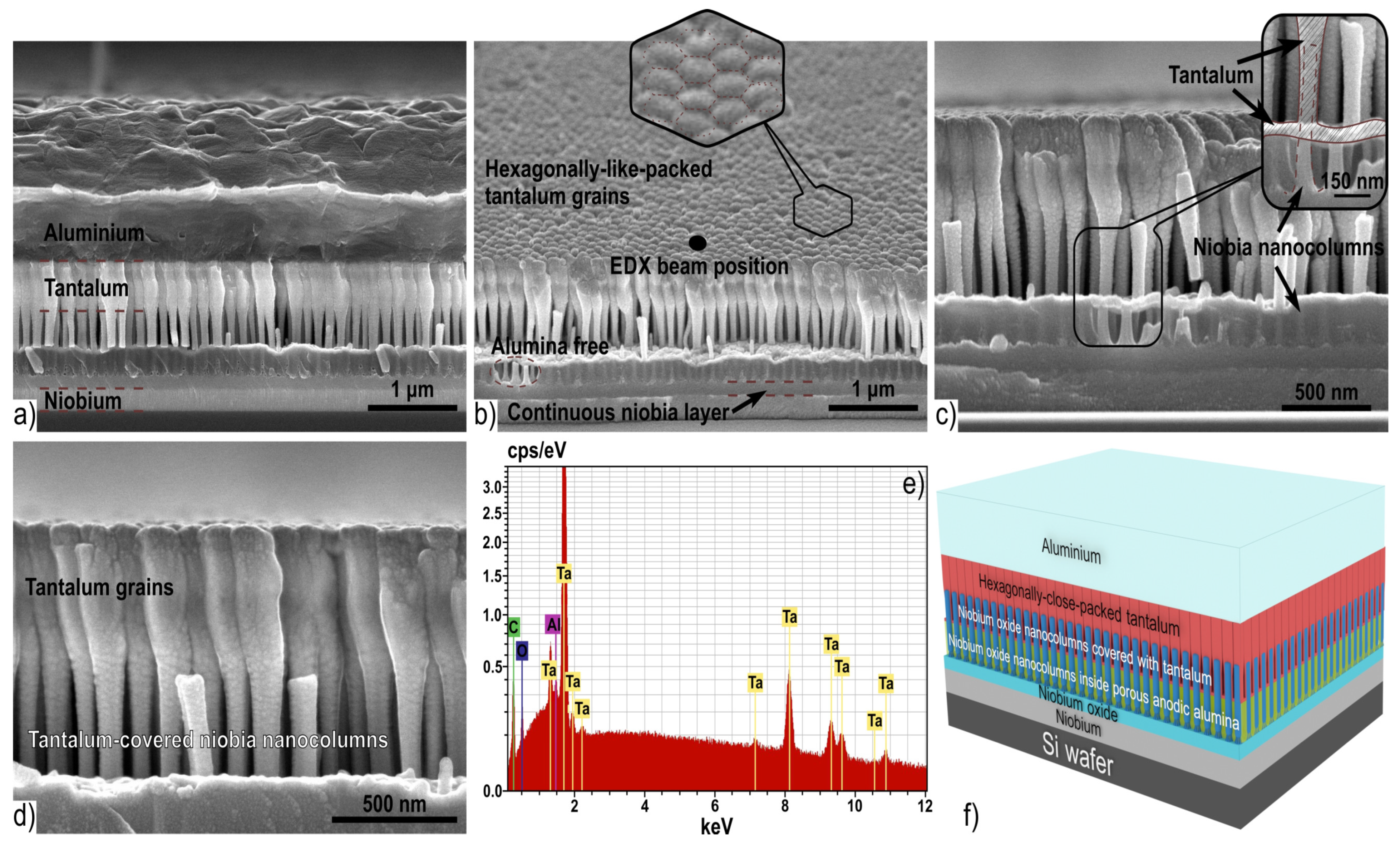
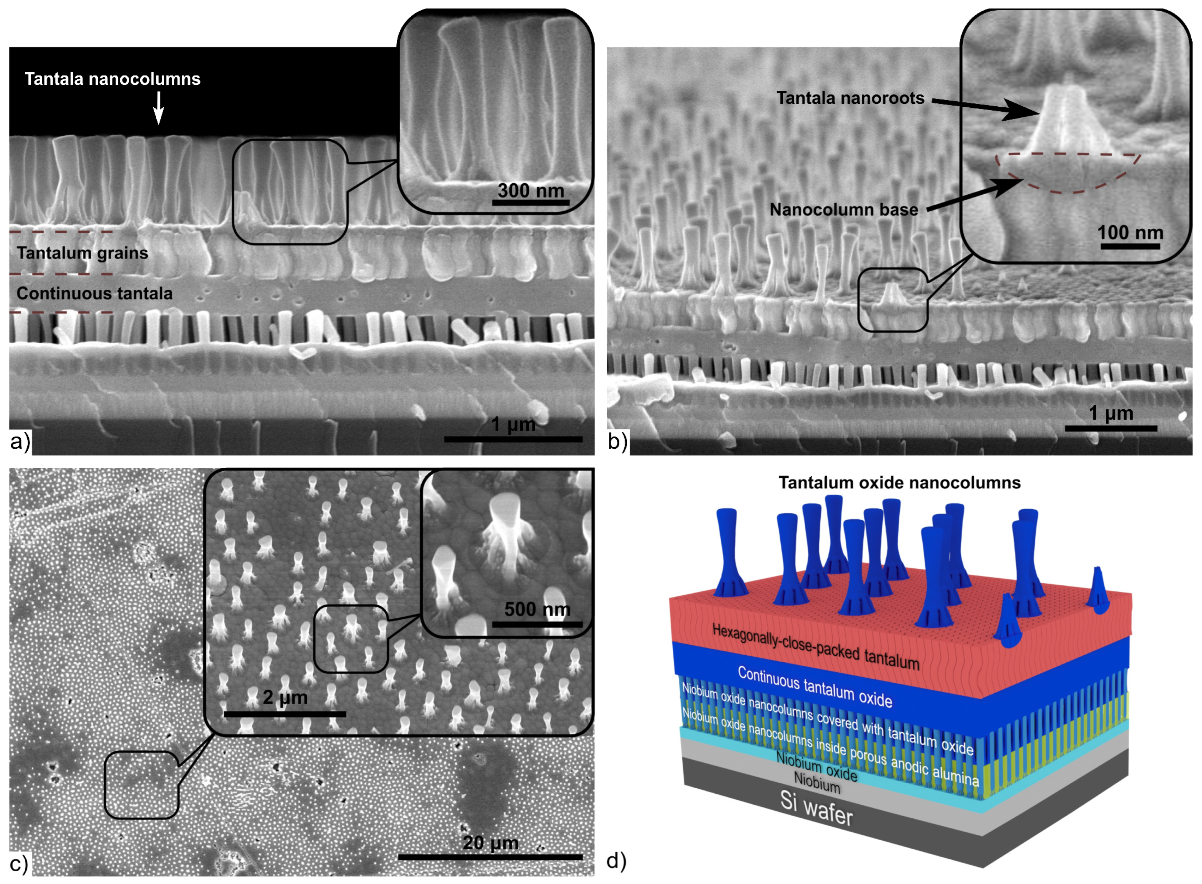
- The first-level column-like 3D nanofilm was coated with an Al/Ta bilayer. The tantalum layer covered the remaining aluminum layer and the walls of the niobia columns, and was nanostructured into a single continuous layer on the surface of these columns, repeating their arrangement. For the first time, hexagonally-packed tantalum was obtained, repeating the hexagonal structure of PAA on the surface of niobia columns.
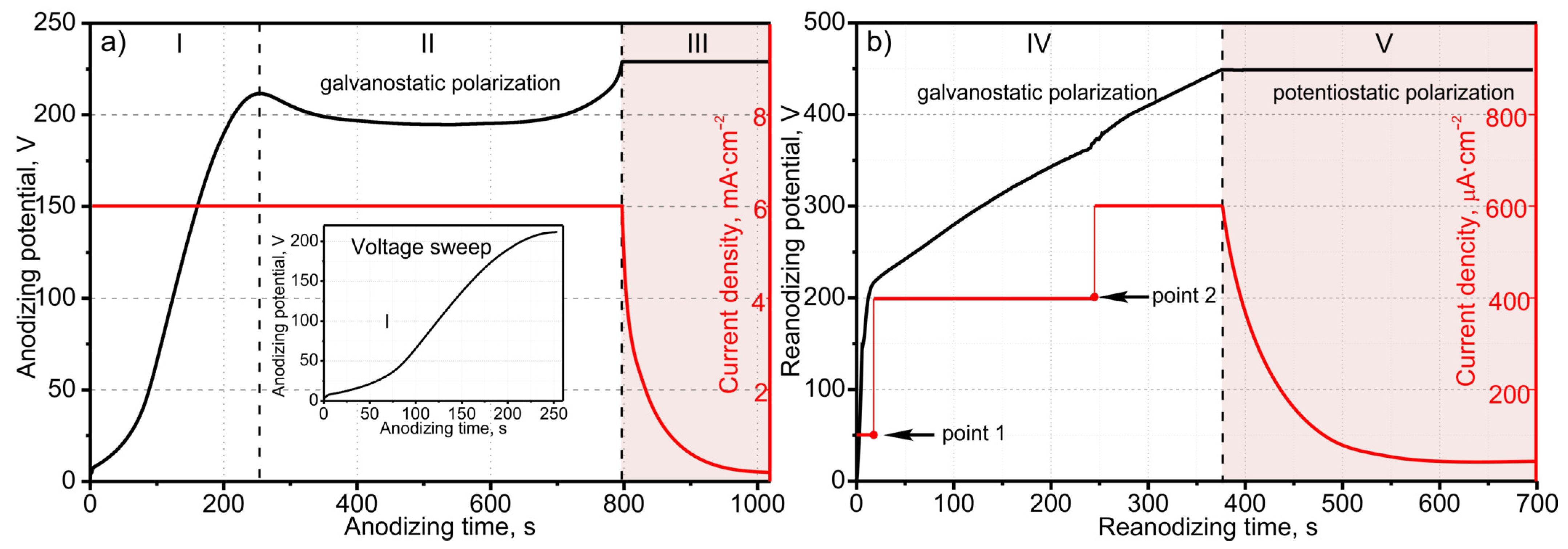
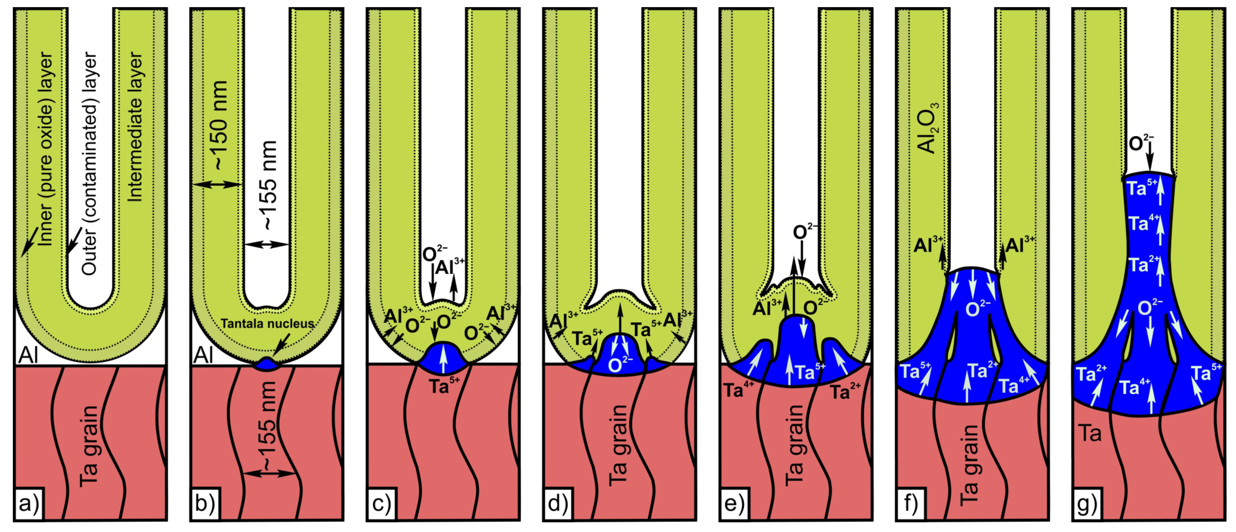
- A second-level column-like 3D nanofilm was formed by anodizing the hexagonally-packed tantalum nanofilm through the PAA. The base of each column of tantala has a characteristic structure consisting of 4–6 roots. The first appearance below the layer of the continuous tantala layer is characterized by high homogeneity and planarity without borders and transitions. The experimental data justified the proposed model of a second-level columnar 3D nanofilm grown from hexagonally-packed tantalum nanofilm, involving field-assisted ionic transport and proper solid-state reactions.
- Long-term chemical etching of the two-level column-like 3D nanofilms for ~24 h in 50% aqueous phosphoric acid resulted in a complete removal on the first- and the second-level of PAA, leading to the formation and condensation of aluminum phosphates and hydrophosphates into nanoparticles, with their subsequent precipitation.
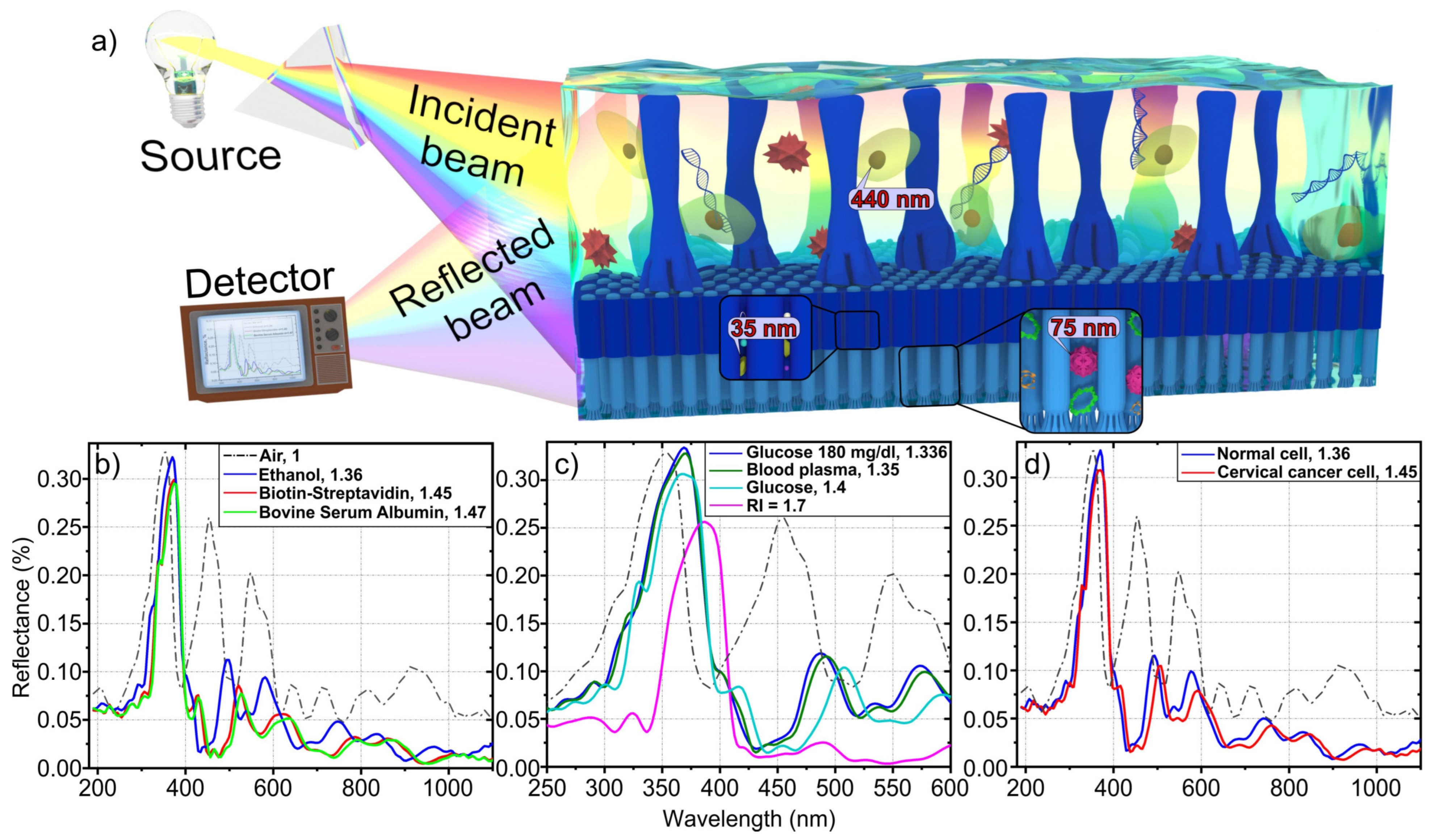
- The fabrication process reported here can result into two-level column-like 3D nanofilms with embedded oxide nanocolumns of various length, width, type of oxides and their relative population, all of which can be tuned by the respective PAA previously formed, according to the respective conditions. These two-level column-like 3D nanofilms appear promising for applications in photonic crystals for full-color displays, chemical sensors and biosensors, solar cells and thermoresponsive shape memory polymer devices. This fabrication technique makes it possible to integrate these dielectric layers with anodically fabricated planar thermoresistors, capacitors and nanowires, as demonstrated in former reports.
Supplementary Materials
Author Contributions
Funding
Institutional Review Board Statement
Informed Consent Statement
Data Availability Statement
Acknowledgments
Conflicts of Interest
References
- Vorobyova, A.I.; Sokol, V.A.; Outkina, E.A. SEM investigation of pillared microstructures formed by electrochemical anodization. Appl. Phys. A Mater. Sci. Process. 1998, 67, 487–492. [Google Scholar] [CrossRef]
- Vorobyova, A.; Outkina, E. Study of pillar microstructure formation with anodic oxides. Thin Solid Films 1998, 324, 1–10. [Google Scholar] [CrossRef]
- Surganov, V.F.; Gorokh, G.G. Array of niobium nanotips formed in porous anodic alumina matrix. In Proceedings of the SPIE 4019, Design, Test, Integration, and Packaging of MEMS/MOEMS, Paris, France, 10 April 2000; pp. 526–530. [Google Scholar]
- Mozalev, A.; Surganov, A.; Magaino, S. Anodic process for forming nanostructured metal-oxide coatings for large-value precise microfilm resistor fabrication. Electrochim. Acta 1999, 44, 3891–3898. [Google Scholar] [CrossRef]
- Pligovka, A.N.; Luferov, A.N.; Nosik, R.F.; Mozalev, A.M. Dielectric characteristics of thin film capacitors based on anodized Al/Ta layers. In Proceedings of the 2010 20th International Crimean Conference ‘Microwave & Telecommunication Technology’, Sevastopol, Ukraine, 13–17 September 2010; pp. 880–881. [Google Scholar]
- Mozalev, A.M.; Plihauka, A.N.; Luferov, A.N.; Popichev, E.L. High frequency characteristics of MIM capacitors with nanostructured anodic oxide dielectrics. In Proceedings of the KpbiMuKo 2009 CriMiCo—2009 19th International Crimean Conference Microwave and Telecommunication Technology, Conference Proceedings, Sevastopol, Ukraine, 14–18 September 2009; pp. 653–654. [Google Scholar]
- Pytlicek, Z.; Bendova, M.; Prasek, J.; Mozalev, A. On-chip sensor solution for hydrogen gas detection with the anodic niobium-oxide nanorod arrays. Sens. Actuators B Chem. 2019, 284, 723–735. [Google Scholar] [CrossRef]
- Mozalev, A.; Bendova, M.; Vazquez, R.M.M.; Pytlicek, Z.; Llobet, E.; Hubalek, J. Formation and gas-sensing properties of a porous-alumina-assisted 3-D niobium-oxide nanofilm. Sens. Actuators B Chem. 2016, 229, 587–598. [Google Scholar] [CrossRef]
- Pligovka, A.; Lazavenka, A.; Gorokh, G. Anodic niobia column-like 3-D nanostructures for semiconductor devices. IEEE Trans. Nanotechnol. 2019, 18, 790–797. [Google Scholar] [CrossRef]
- Gorokh, G.G.; Pligovka, A.N.; Lozovenko, A.A. Columnar niobium oxide nanostructures: Mechanism of formation, microstructure, and electrophysical properties. Tech. Phys. 2019, 64, 1657–1665. [Google Scholar] [CrossRef]
- Mozalev, A.; Habazaki, H.; Hubálek, J. The superhydrophobic properties of self-organized microstructured surfaces derived from anodically oxidized Al/Nb and Al/Ta metal layers. Electrochim. Acta 2012, 82, 90–97. [Google Scholar] [CrossRef]
- Pligovka, A. Reflectant photonic crystals produced via porous-alumina-assisted-anodizing of Al/Nb and Al/Ta systems. Surf. Rev. Lett. 2021, 28, 2150055. [Google Scholar] [CrossRef]
- Pligovka, A.; Poznyak, A.; Norek, M. Optical Properties of porous alumina assisted niobia nanostructured films—Designing 2-D photonic crystals based on hexagonally arranged nanocolumns. Micromachines 2021, 12, 589. [Google Scholar] [CrossRef]
- Mozalev, A.; Smith, A.J.; Borodin, S.; Plihauka, A.; Hassel, A.W.; Sakairi, M.; Takahashi, H. Growth of multioxide planar film with the nanoscale inner structure via anodizing Al/Ta layers on Si. Electrochim. Acta 2009, 54, 935–945. [Google Scholar] [CrossRef]
- Pligovka, A.; Yunin, P.; Hoha, A.; Korolyov, S.; Gorokh, G.; Skorokhodov, E. Morphology and structure of defected niobium oxide nonuniform arrays formed by anodizing bilayer Al/Nb systems. Tech. Phys. 2020, 65, 1771–1776. [Google Scholar] [CrossRef]
- Pligovka, A.; Hoha, A.; Turavets, U.; Poznyak, A.; Zakharau, Y. Formation features, morphology and optical properties of nanostructures via anodizing Al/Nb on Si and glass. Mater. Today Proc. 2021, 37, A8–A15. [Google Scholar] [CrossRef]
- Pligovka, A.; Zakhlebayeva, A.; Lazavenka, A. Niobium oxide nanocolumns formed via anodic alumina with modulated pore diameters. J. Phys. Conf. Ser. 2018, 987, 012006. [Google Scholar] [CrossRef]
- Mozalev, A.; Bendova, M.; Gispert-Guirado, F.; Llobet, E. Hafnium-oxide 3-D nanofilms via the anodizing of Al/Hf metal layers. Chem. Mater. 2018, 30, 2694–2708. [Google Scholar] [CrossRef]
- Bendova, M.; Kolar, J.; Marik, M.; Lednicky, T.; Mozalev, A. Influence of nitrogen species on the porous-alumina-assisted growth of TiO2 nanocolumn arrays. Electrochim. Acta 2018, 281, 796–809. [Google Scholar] [CrossRef]
- Bendova, M.; Gispert-Guirado, F.; Hassel, A.W.; Llobet, E.; Mozalev, A. Solar water splitting on porous-alumina-assisted TiO2-doped WOx nanorod photoanodes: Paradoxes and challenges. Nano Energy 2017, 33, 72–87. [Google Scholar] [CrossRef]
- Mozalev, A.; Khatko, V.; Bittencourt, C.; Hassel, A.W.; Gorokh, G.; Llobet, E.; Correig, X. Nanostructured columnlike tungsten oxide film by anodizing Al/W/Ti layers on Si. Chem. Mater. 2008, 20, 6482–6493. [Google Scholar] [CrossRef]
- Calavia, R.; Mozalev, A.; Kahtko, V.; Gorokh, G.; Vilanova, X.; Correig, X.; Gracia, I.; Cane, C.; Llobet, E. AH2 microsensor based on nanocolumnar tungsten oxide grown by template-assisted anodization. In Proceedings of the TRANSDUCERS 2009–2009 International Solid-State Sensors, Actuators and Microsystems Conference, Denver, CO, USA, 21–25 June 2009; pp. 1313–1316. [Google Scholar]
- Bendova, M.; Hubalek, J.; Mozalev, A. Exploring electron transport and memristive switching in nanoscale Au/WOx/W multijunctions based on anodically oxidized Al/W metal layers. Adv. Mater. Interfaces 2016, 3, 1600512. [Google Scholar] [CrossRef]
- Mozalev, A.; Mozaleva, I.; Sakairi, M.; Takahashi, H. Anodic film growth on Al layers and Ta-Al metal bilayers in citric acid electrolytes. Electrochim. Acta 2005, 50, 5065–5075. [Google Scholar] [CrossRef]
- Mozalev, A.; Hubalek, J. On-substrate porous-anodic-alumina-assisted gold nanostructure arrays: Meeting the challenges of various sizes and interfaces. Electrochim. Acta 2019, 297, 988–999. [Google Scholar] [CrossRef]
- Bogomazova, N.; Gorokh, G.; Zakhlebayeva, A.; Pligovka, A.; Murashkevich, A.; Galkovsky, T. Photosensitive sulphide heterostructures obtained by using successive ionic layer adsorption and reaction on planar and profiled substrates. J. Phys. Conf. Ser. 2018, 1124, 81032. [Google Scholar] [CrossRef]
- Mozalev, A.; Sakairi, M.; Takahashi, H. Structure, morphology, and dielectric properties of nanocomposite oxide films formed by anodizing of sputter-deposited Ta-Al bilayers. J. Electrochem. Soc. 2004, 151, F257. [Google Scholar] [CrossRef]
- Mozalev, A.; Vázquez, R.M.; Bittencourt, C.; Cossement, D.; Gispert-Guirado, F.; Llobet, E.; Habazaki, H. Formation-structure-properties of niobium-oxide nanocolumn arrays via self-organized anodization of sputter-deposited aluminum-on-niobium layers. J. Mater. Chem. C 2014, 2, 4847–4860. [Google Scholar] [CrossRef]
- Lee, W.; Park, S.-J.J. Porous anodic aluminum oxide: Anodization and templated synthesis of functional nanostructures. Chem. Rev. 2014, 114, 7487–7556. [Google Scholar] [CrossRef] [PubMed]
- Mozalev, A.; Sakairi, M.; Saeki, I.; Takahashi, H. Nucleation and growth of the nanostructured anodic oxides on tantalum and niobium under the porous alumina film. Electrochim. Acta 2003, 48, 3155–3170. [Google Scholar] [CrossRef]
- Vázquez, R.M.; Mozalev, A.; Llobet, E. Fast response hydrogen microsensor based on semiconductor niobium-oxide nanostructures via smart anodizing of Al/Nb metal layers. Procedia Eng. 2014, 87, 811–814. [Google Scholar] [CrossRef]
- Law, C.S.; Lim, S.Y.; Abell, A.D.; Voelcker, N.H.; Santos, A. Nanoporous anodic alumina photonic crystals for optical chemo- and biosensing: Fundamentals, advances, and perspectives. Nanomaterials 2018, 8, 788. [Google Scholar] [CrossRef]
- CRC Handbook of Chemistry and Physics; Haynes, W.M., Lide, D.R., Bruno, T.J., Eds.; CRC Press: Boca Raton, FL, USA, 2016; ISBN 9781315380476. [Google Scholar]
- Φизичecкиe вeличины: Cпpaвoчник; Гpигopьeвa, И.C., Meйлихoвa, E.З., Eds.; Энepгoaтoмиздaт: Mocквa, Russia, 1991; ISBN 5-283-04013-5. [Google Scholar]
- Robinson, M.L.A.; Roetschi, H.A.C. polarisation in B-modification Nb2O5 single crystals. J. Phys. Chem. Solids 1968, 29, 1503–1510. [Google Scholar] [CrossRef]
- Pignolet, A.; Rao, G.M.; Krupanidhi, S.B. Rapid thermal processed thin films of niobium pentoxide (Nb2O5) deposited by reactive magnetron sputtering. Thin Solid Films 1995, 261, 18–24. [Google Scholar] [CrossRef]
- Chalker, P.R.; Werner, M.; Romani, S.; Potter, R.J.; Black, K.; Aspinall, H.C.; Jones, A.C.; Zhao, C.Z.; Taylor, S.; Heys, P.N. Permittivity enhancement of hafnium dioxide high-κ films by cerium doping. Appl. Phys. Lett. 2008, 93, 182911. [Google Scholar] [CrossRef]
- Han, X.Y.; Shen, W.Z. Improved two-step anodization technique for ordered porous anodic aluminum membranes. J. Electroanal. Chem. 2011, 655, 56–64. [Google Scholar] [CrossRef]
- Choi, J.; Nielsch, K.; Reiche, M.; Wehrspohn, R.B.; Gösele, U. Fabrication of monodomain alumina pore arrays with an interpore distance smaller than the lattice constant of the imprint stamp. J. Vac. Sci. Technol. B Microelectron. Nanom. Struct. 2003, 21, 763. [Google Scholar] [CrossRef]
- Zhao, Y.; Zhang, Z.; Lin, Y. Optical and dielectric properties of a nanostructured NbO2 thin film prepared by thermal oxidation. J. Phys. D. Appl. Phys. 2004, 37, 3392–3395. [Google Scholar] [CrossRef]
- Kerrec, O.; Devilliers, D.; Groult, H.; Chemla, M. Dielectric properties of anodic oxide films on tantalum. Electrochim. Acta 1995, 40, 719–724. [Google Scholar] [CrossRef]
- Ye, Y.; Chen, C.; Bai, H.; Liu, W.; Li, W.; Li, J.; Yi, W.; Xi, G. Quasi-metallic tungsten oxide nanodendrites with high stability for surface-enhanced raman scattering. Cell Rep. Phys. Sci. 2020, 1, 100031. [Google Scholar] [CrossRef]
- Gao, L.; Lemarchand, F.; Lequime, M. Exploitation of multiple incidences spectrometric measurements for thin film reverse engineering. Opt. Express 2012, 20, 15734. [Google Scholar] [CrossRef]
- Masuda, H.; Satoh, M. Fabrication of gold nanodot array using anodic porous alumina as an evaporation mask. Jpn. J. Appl. Phys. 1996, 35, L126–L129. [Google Scholar] [CrossRef]
- Young, L. Anodization constants for tantalum. J. Electrochem. Soc. 1977, 124, 528–529. [Google Scholar] [CrossRef]
- Wagh, A.S.; Jeong, S.Y. Chemically bonded phosphate ceramics: I, A dissolution model of formation. J. Am. Ceram. Soc. 2003, 86, 1838–1844. [Google Scholar] [CrossRef]
- Gonzalez, F.; Halloran, J. Reaction of orthophosphoric acid with several forms of aluminum oxide. Am. Ceram. Soc. Bull. 1980, 59, 727–738. [Google Scholar]
- Wagh, A.S.; Grover, S.; Jeong, S.Y. Chemically bonded phosphate ceramics: II, warm-temperature process for alumina ceramics. J. Am. Ceram. Soc. 2003, 86, 1845–1849. [Google Scholar] [CrossRef]
- Sharma, P.; Roy, S.K.; Sharan, P. Design and simulation of photonic crystal based biosensor for detection of different blood components. In Proceedings of the 2014 IEEE REGION 10 SYMPOSIUM, Kuala Lumpur, Malaysia, 14–16 April 2014; pp. 171–176. [Google Scholar]
- Sundhar, A.; Valli, R.; Robinson, S.; Abinayaa, A.; SivaBharathy, C. Two Dimensional Photonic Crystal Based Bio Sensor for Cancer Cell Detection. In Proceedings of the 2019 IEEE International Conference on System, Computation, Automation and Networking (ICSCAN), Pondicherry, India, 29–30 March 2019; pp. 1–3. [Google Scholar]
- Yashaswini, P.R.; Gayathri, H.N.; Srikanth, P.C. Performance analysis of photonic crystal based biosensor for the detection of bio-molecules in urine and blood. Mater. Today Proc. 2021, in press. [Google Scholar] [CrossRef]

| Parameter | Value |
|---|---|
| Aluminum thickness (nm) | 1200 |
| Niobium thickness (nm) | 300 |
| Anodizing/reanodizing voltage (V) | 53/450 |
| PAA thickness (nm) | 163 |
| Average diameter of PAA cell (nm) | 130 |
| Niobium metal thickness (nm) | 198 |
| Continuous niobia thickness (Hlow, nm) | 122 |
| Height of niobia columns (Hup, nm) | 444 |
| Distance between column centers (nm) | 129 |
| Average diameter of niobia columns (nm) | 57 |
| Parameter | Value |
|---|---|
| Continuous tantalum layer height (nm) | 426 |
| Average tantalum grain diameter (nm) | 120 |
| Distance between continuous tantalum and Ta layer on PAA (nm) | 340 |
| Anodizing/reanodizing voltage (V) | 200/450 |
| Height of tantala columns (Hup, nm) | 635 |
| Minimum diameter of column (Dlow, nm) | 90 |
| Maximum diameter of columns (Dhigh, nm) | 145 |
| Diameter of tantala columns base (nm) | 359 |
| Distance between column centers (nm) | 556 |
| Continuous structured Ta metal layer (nm) | 364 |
| Continuous tantala layer (nm) | 282 |
| Tantala layer on PAA (nm) | 87 |
| Element | Atomic Number | Series | Unn.C [wt.%] | Norm.C [wt.%] | Unn.C [at.%] | Error [wt.%] |
|---|---|---|---|---|---|---|
| Carbon | 6 | K-series | 10.76 | 11.40 | 57.57 | 1.7 |
| Oxygen | 8 | K-series | 3.03 | 3.21 | 12.16 | 0.6 |
| Aluminum | 13 | K-series | 0.81 | 0.86 | 1.92 | 0.1 |
| Tantalum | 73 | L-series | 79.79 | 84.54 | 28.34 | 2.7 |
| Total: | 94.39 | 100.00 | 100.00 |
Disclaimer/Publisher’s Note: The statements, opinions and data contained in all publications are solely those of the individual author(s) and contributor(s) and not of MDPI and/or the editor(s). MDPI and/or the editor(s) disclaim responsibility for any injury to people or property resulting from any ideas, methods, instructions or products referred to in the content. |
© 2023 by the authors. Licensee MDPI, Basel, Switzerland. This article is an open access article distributed under the terms and conditions of the Creative Commons Attribution (CC BY) license (https://creativecommons.org/licenses/by/4.0/).
Share and Cite
Pligovka, A.; Lazavenka, A.; Turavets, U.; Hoha, A.; Salerno, M. Two-Level 3D Column-like Nanofilms with Hexagonally–Packed Tantalum Fabricated via Anodizing of Al/Nb and Al/Ta Layers—A Potential Nano-Optical Biosensor. Materials 2023, 16, 993. https://doi.org/10.3390/ma16030993
Pligovka A, Lazavenka A, Turavets U, Hoha A, Salerno M. Two-Level 3D Column-like Nanofilms with Hexagonally–Packed Tantalum Fabricated via Anodizing of Al/Nb and Al/Ta Layers—A Potential Nano-Optical Biosensor. Materials. 2023; 16(3):993. https://doi.org/10.3390/ma16030993
Chicago/Turabian StylePligovka, Andrei, Andrei Lazavenka, Ulyana Turavets, Alexander Hoha, and Marco Salerno. 2023. "Two-Level 3D Column-like Nanofilms with Hexagonally–Packed Tantalum Fabricated via Anodizing of Al/Nb and Al/Ta Layers—A Potential Nano-Optical Biosensor" Materials 16, no. 3: 993. https://doi.org/10.3390/ma16030993
APA StylePligovka, A., Lazavenka, A., Turavets, U., Hoha, A., & Salerno, M. (2023). Two-Level 3D Column-like Nanofilms with Hexagonally–Packed Tantalum Fabricated via Anodizing of Al/Nb and Al/Ta Layers—A Potential Nano-Optical Biosensor. Materials, 16(3), 993. https://doi.org/10.3390/ma16030993


