
Research Progress of Electroplated Nanotwinned Copper in Microelectronic Packaging


Abstract
:1. Introduction
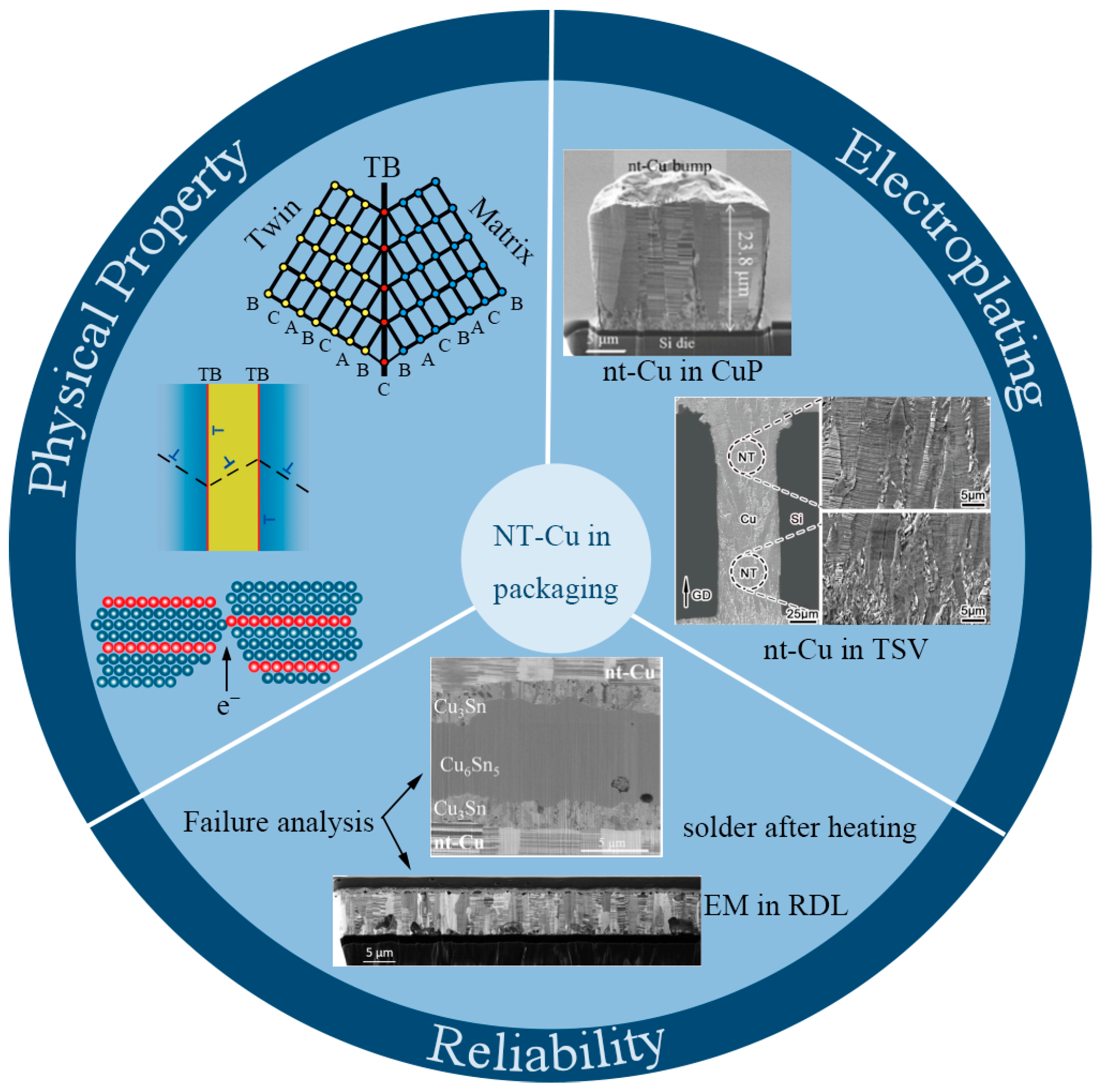
2. Microstructure and Property Optimization of nt-Cu
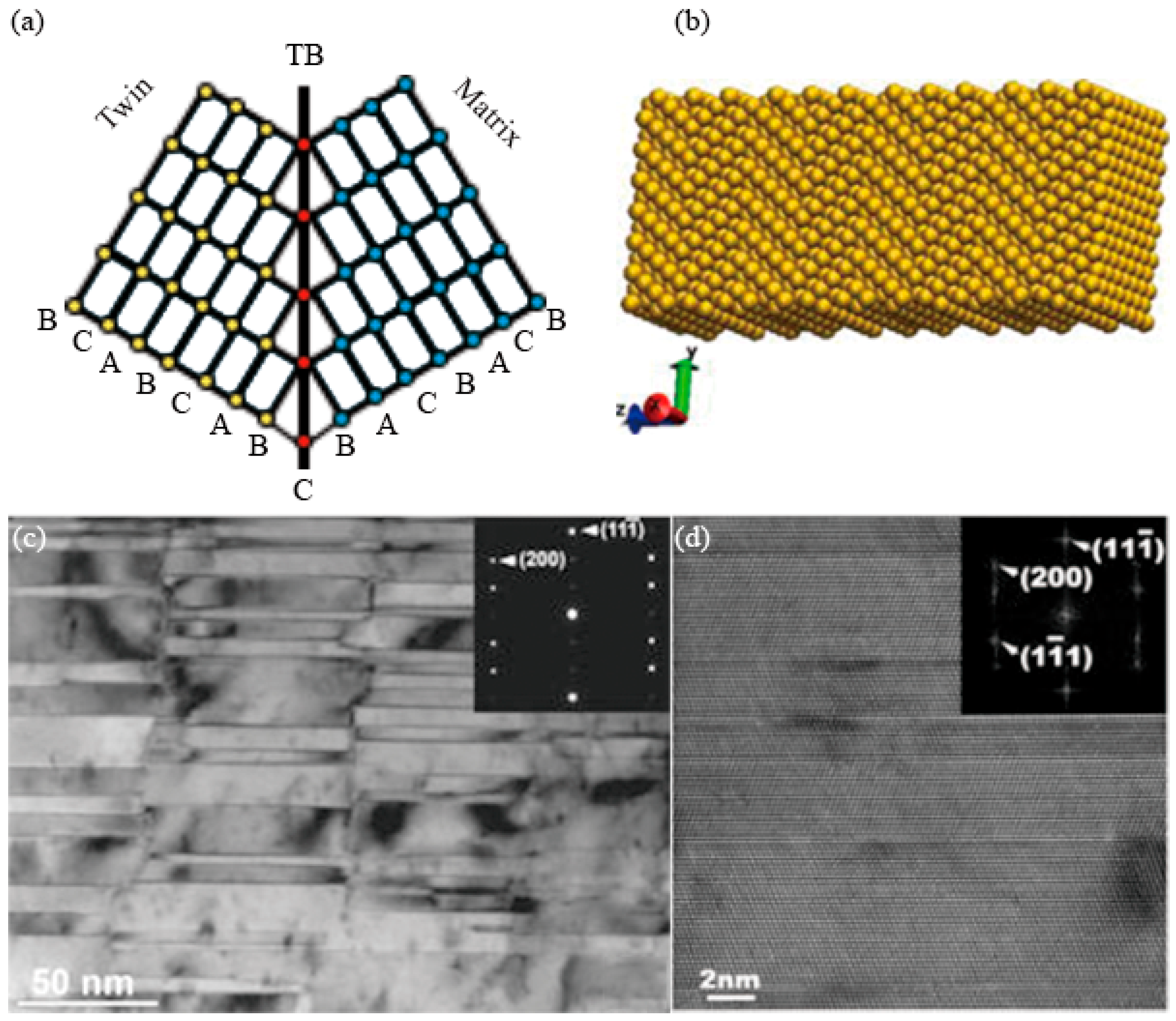
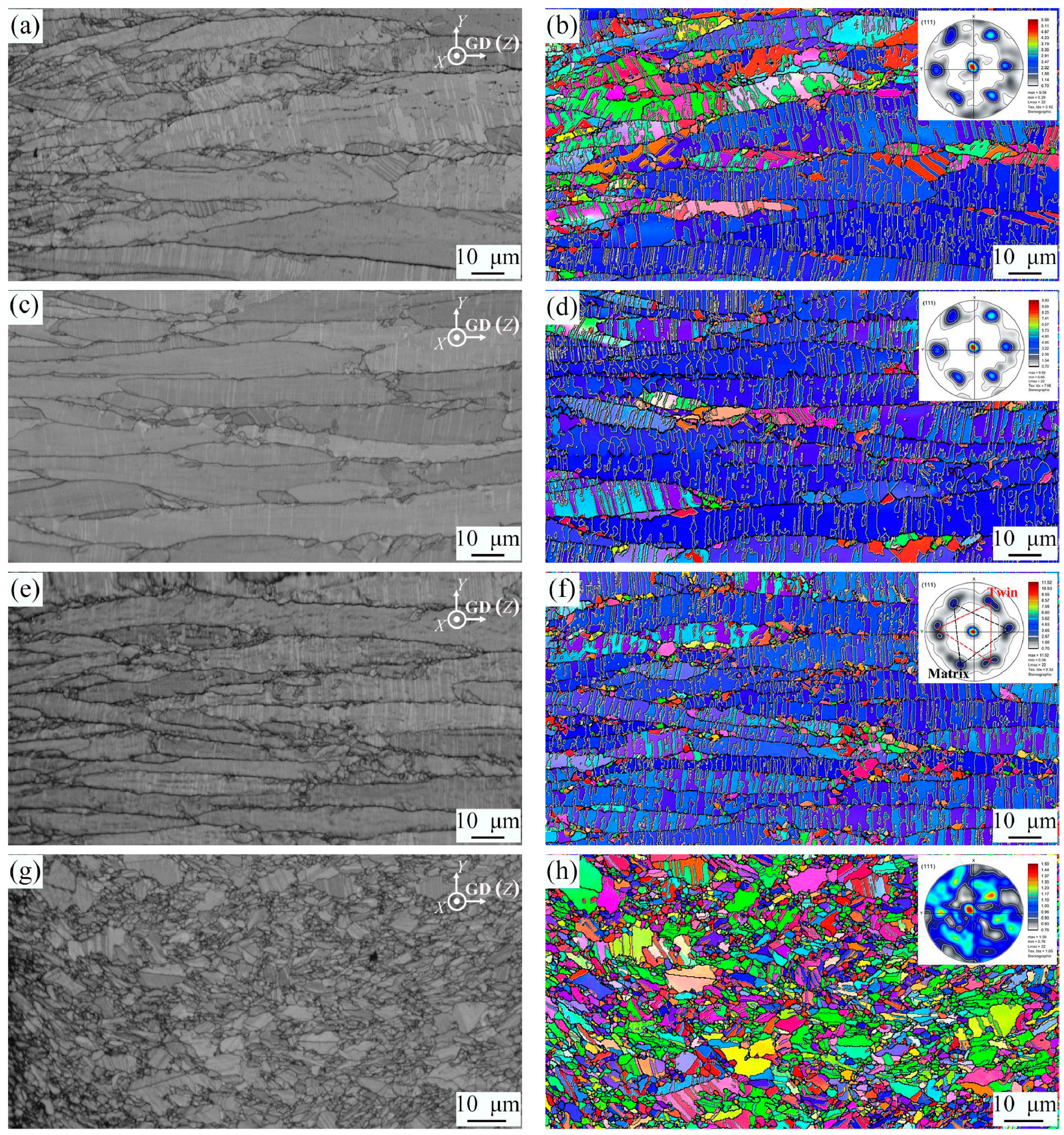
2.1. Lattice and Atomic Arrangement of nt-Cu
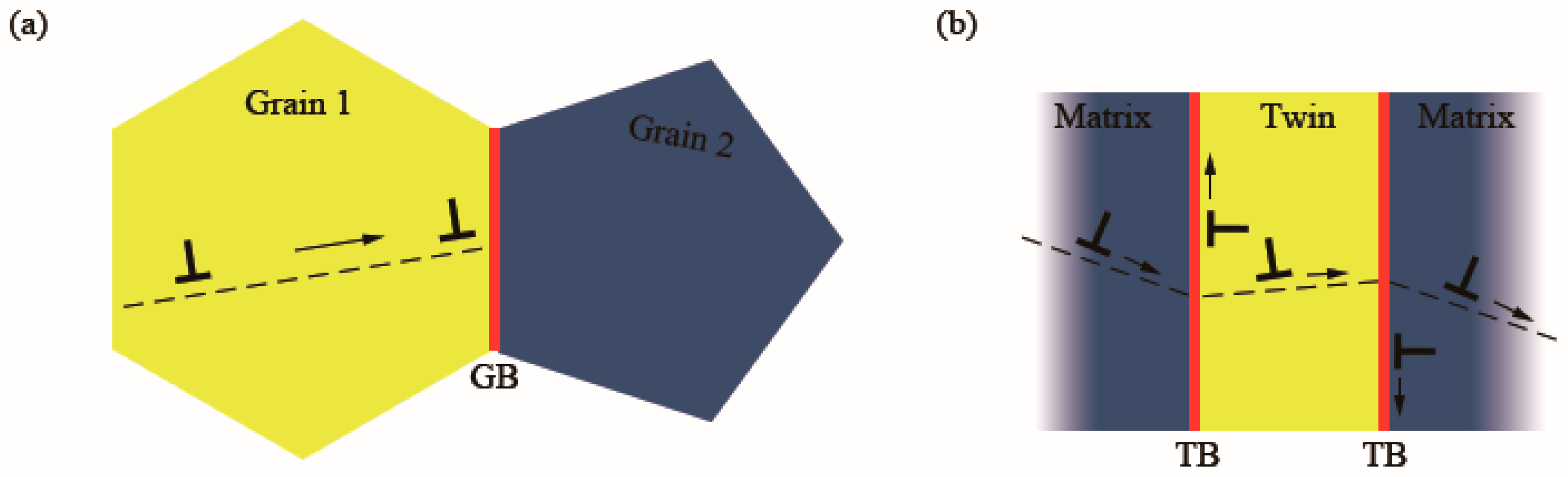
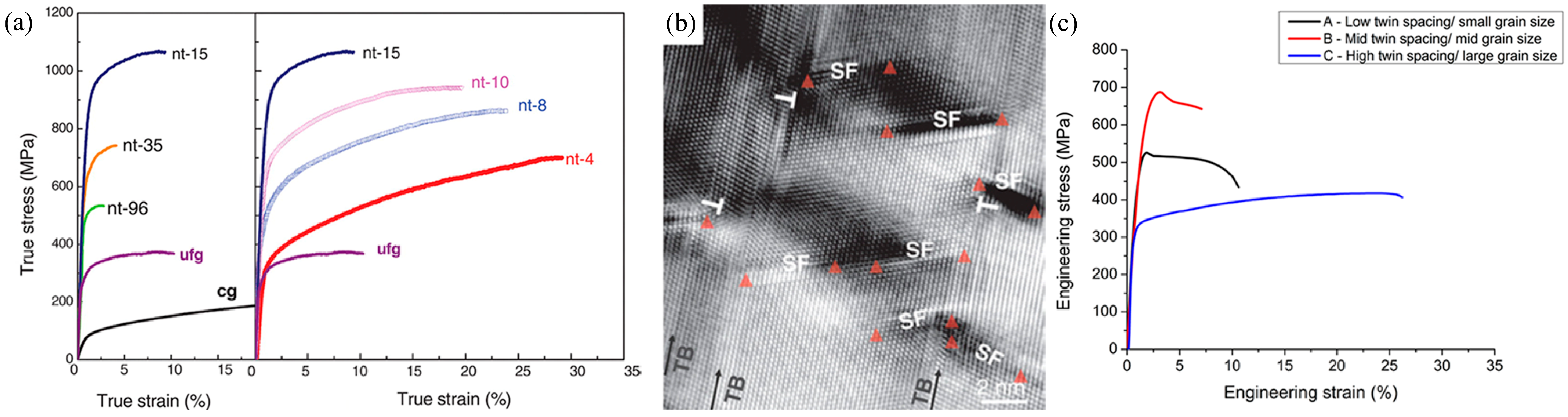
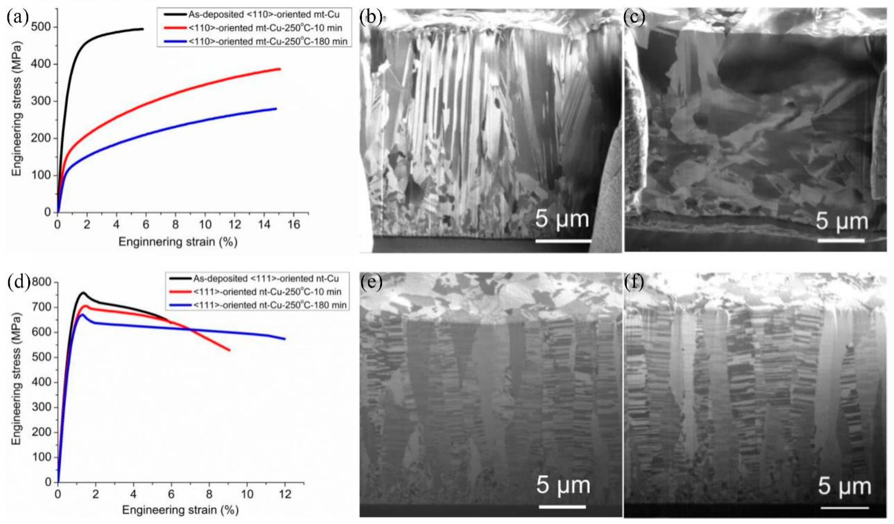
2.2. Mechanical Properties of nt-Cu
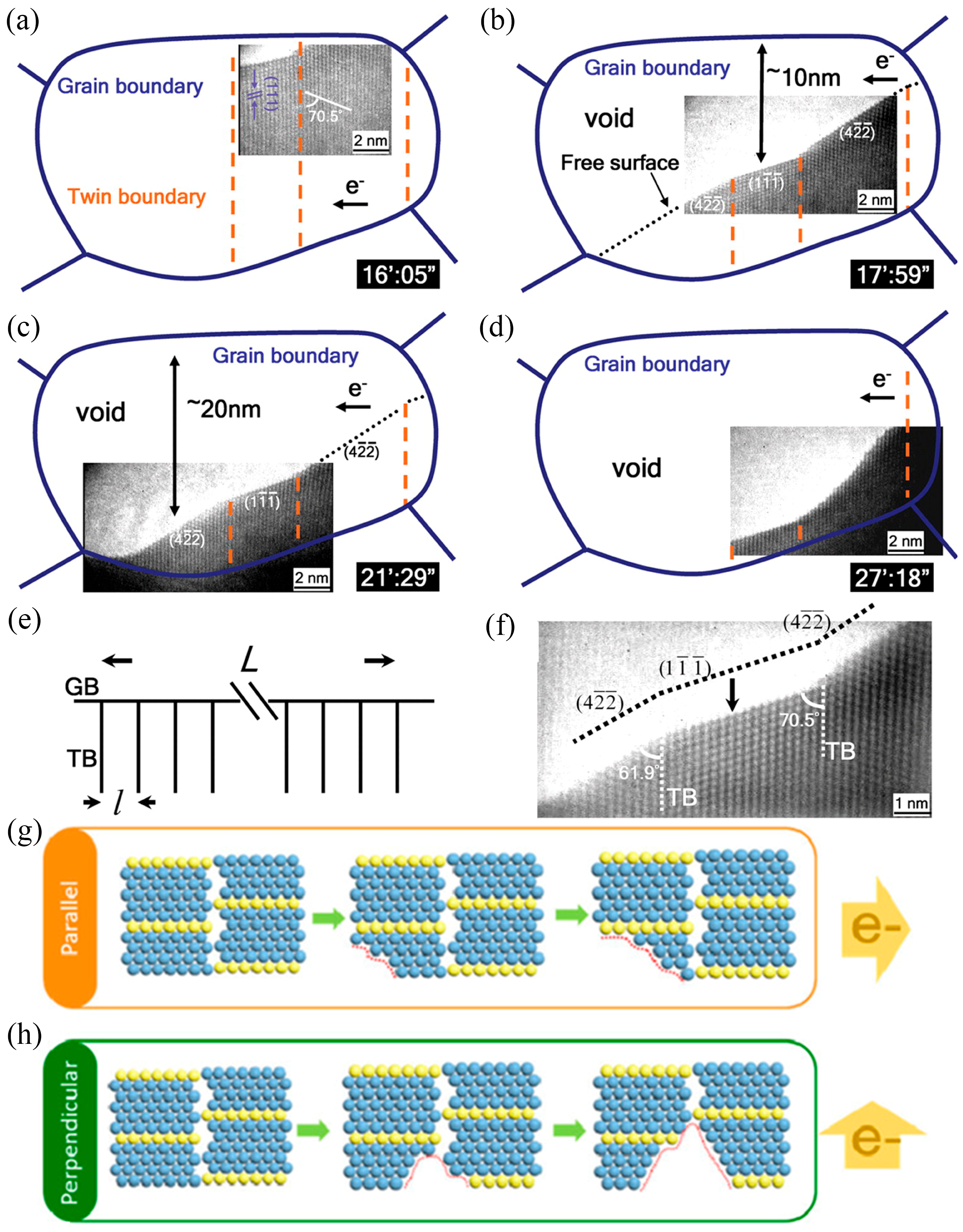
2.3. Electrical Properties of nt-Cu
2.4. Thermal Stability and Corrosion and Oxidation Resistance of nt-Cu
3. Electroplating nt-Cu in the Field of Microelectronic Packaging
3.1. Electroplating Process of nt-Cu
3.1.1. Effect of Pulse Parameters
3.1.2. Effects of Other Influencing Factors
3.2. Electroplating Solutions of nt-Cu
3.2.1. Effect of Acidity
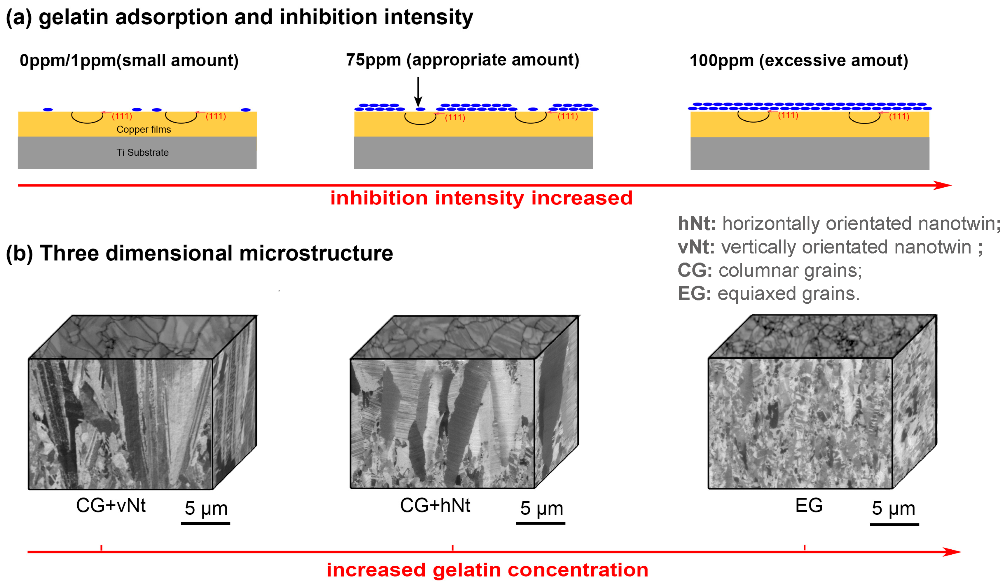
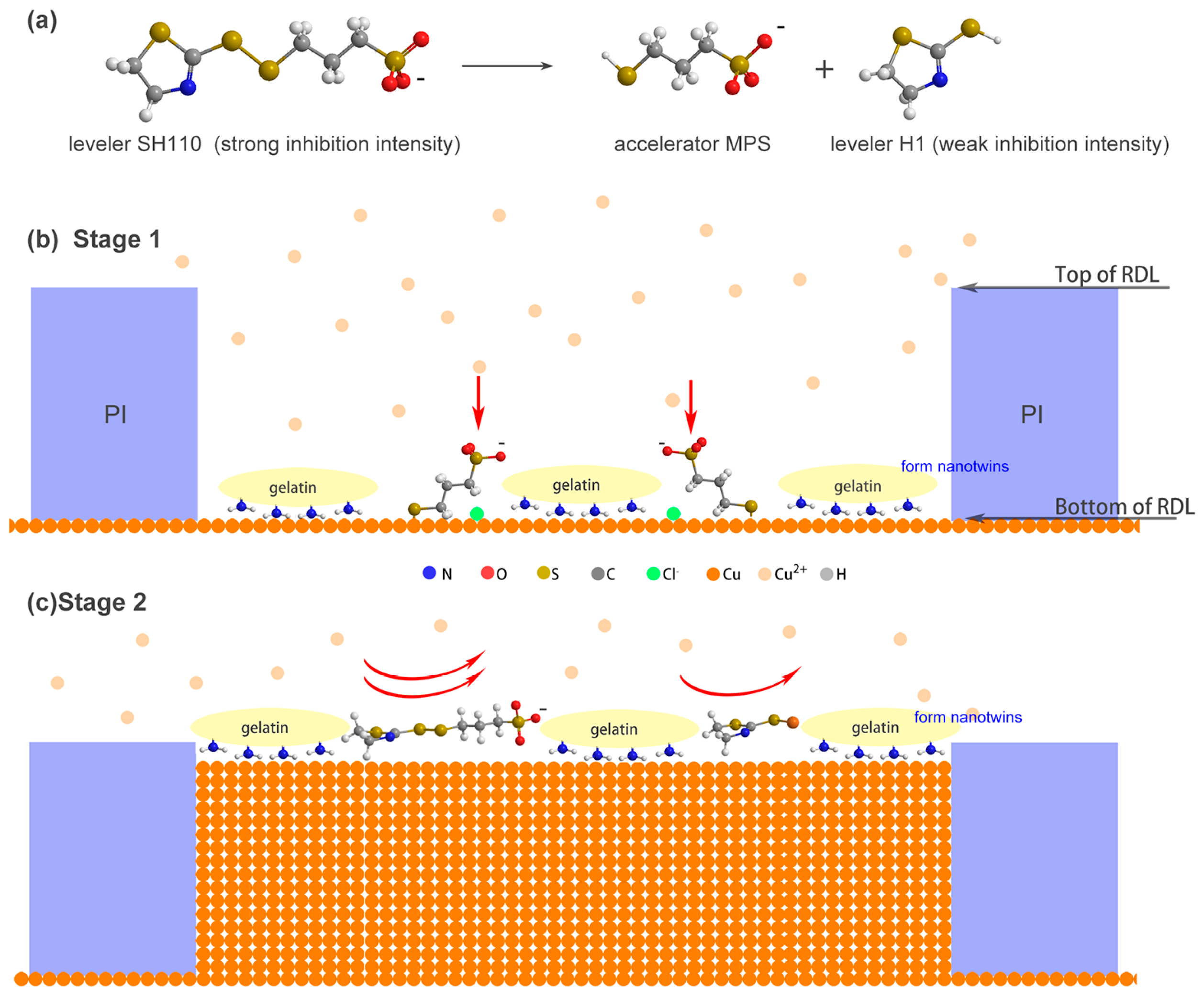
3.2.2. Effect of Additives
3.3. Electroplating nt-Cu Applied in Microelectronic Packaging
4. Reliability of nt-Cu in Electronic Packaging
4.1. Interfacial Reaction Layers
4.2. Redistribution Layers (RDLs)
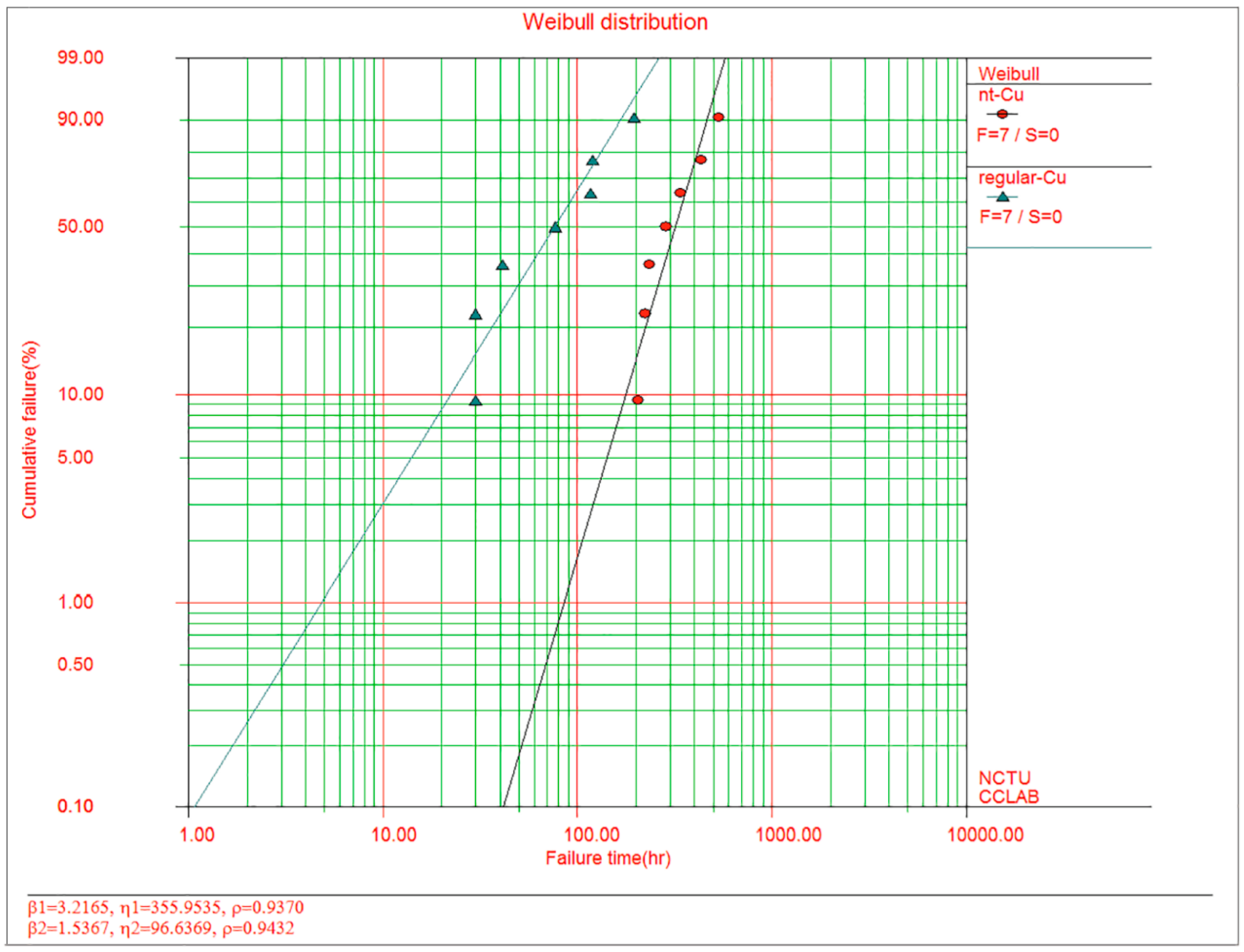
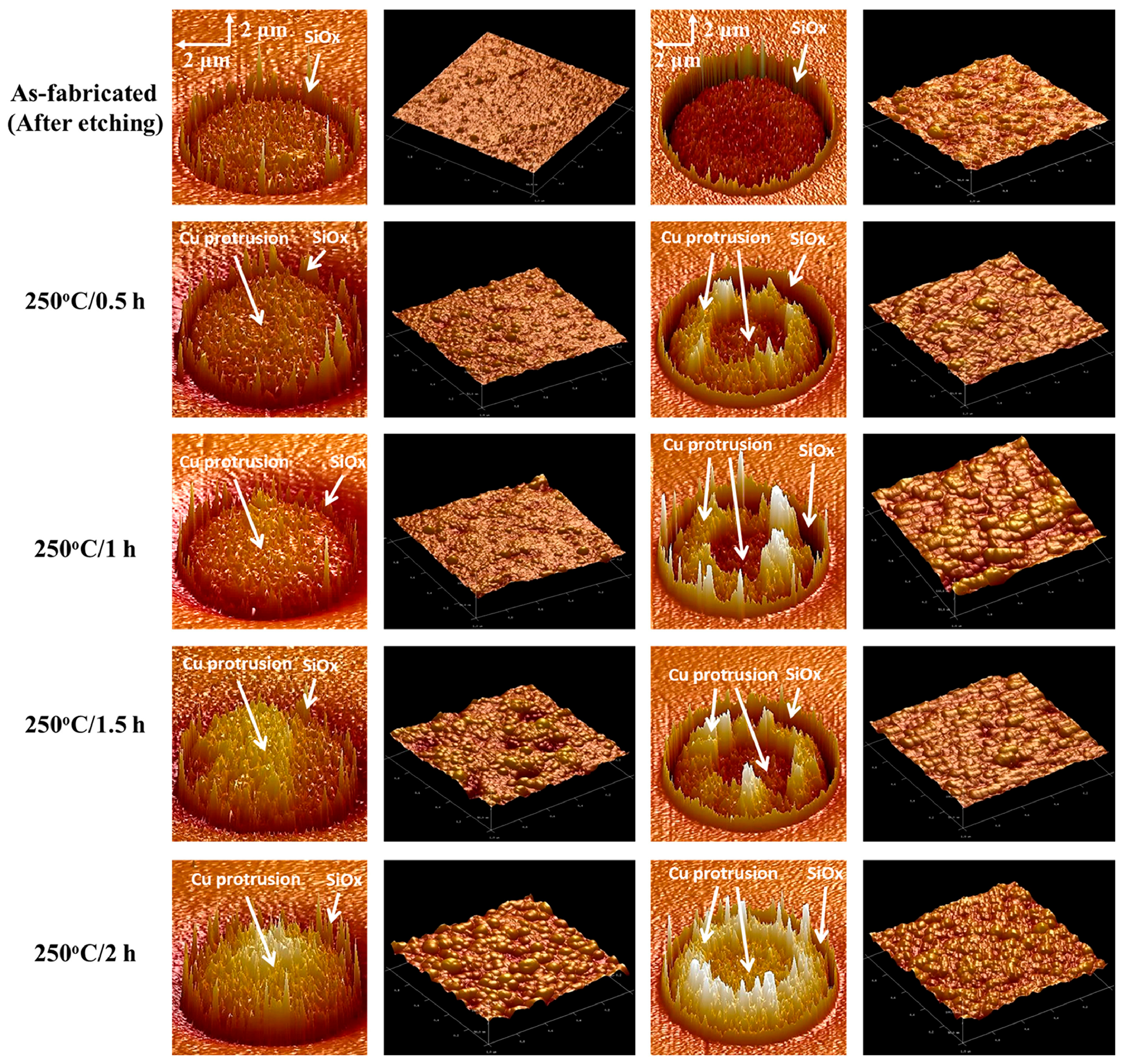
4.3. Through-Silicon Vias (TSVs)
4.4. Other Applications in Microelectronic Packaging
5. Conclusions
- Enhancement of microstructure regularity and reduction of impurity concentration to ensure the good physical properties of nt-Cu under the trend of electronic packaging miniaturization.
- Improvement of the filling performance of nt-Cu electrolytes for different patterns on wafers.
- Evaluation of thorough reliabilities (force, thermal, and electrical aspects) for specific applications.
Author Contributions
Funding
Institutional Review Board Statement
Informed Consent Statement
Data Availability Statement
Conflicts of Interest
References
- Zheng, Z.; Huang, Y.-T.; Wang, Z.; Zhang, M.; Wang, W.-T.; Chung, C.-C.; Cherng, S.-J.; Tsai, Y.-H.; Li, P.-C.; Lu, Z.; et al. Electrodeposition of (111)-oriented and nanotwin-doped nanocrystalline Cu with ultrahigh strength for 3D IC application. Nanotechnology 2021, 32, 225702. [Google Scholar] [CrossRef] [PubMed]
- Lau, J.-H. Heterogeneous Integrations; Springer: Singapore, 2019. [Google Scholar]
- Baklanov, M.R.; Adelmann, C.; Zhao, L.; De Gendt, S. Advanced Interconnects: Materials, Processing, and Reliability. ECS J. Solid State Sci. Technol. 2014, 4, Y1–Y4. [Google Scholar] [CrossRef]
- Cheng, Y.-L.; Lee, C.-Y.; Huang, Y.-L. Copper Metal for Semiconductor Interconnects. In Noble and Precious Metals; Mohindar Singh, S., Alan, D.B., Eds.; IntechOpen: Rijeka, Croatia, 2018. [Google Scholar]
- Wei, Q. Progress in research on carbon nanotubes interconnection. J. Funct. Mater. Devices 2012, 18, 63–69. [Google Scholar]
- Taubenblatt, M.-A. Optical Interconnects for High-Performance Computing. J. Lightwave Technol. 2012, 30, 448–457. [Google Scholar] [CrossRef]
- Amanov, A. Microstructural evolution and mechanical properties of Cu-based alloy by post-sintering ultrasonic nanocrystal surface modification. Mater. Lett. 2022, 308, 131124. [Google Scholar] [CrossRef]
- Zhao, H.-Z.; You, Z.-S.; Tao, N.-R.; Lu, L. Anisotropic toughening of nanotwin bundles in the heterogeneous nanostructured Cu. Acta Mater. 2022, 228, 117748. [Google Scholar] [CrossRef]
- Kou, Z.; Huang, R.; Yang, Y.; Feng, T.; Tang, S.; Lan, S.; Yang, L. Revealing the atomic-scale evolution of sessile disconnections on twin boundaries during deformation. Scr. Mater. 2022, 221, 114956. [Google Scholar] [CrossRef]
- Shi, Z.; Gao, L.-Y.; Zhang, Y.-B.; Liu, Z.-Q. The serving behavior of nanotwinned copper under the reliability test of high temperature high humidity and electromigration test. In Proceedings of the 2022 23rd International Conference on Electronic Packaging Technology (ICEPT), Dalian, China, 10–13 August 2022. [Google Scholar] [CrossRef]
- Lu, L.; Shen, Y.; Chen, X.; Qian, L.; Lu, K. Ultrahigh Strength and High Electrical Conductivity in Copper. Science 2004, 304, 422–426. [Google Scholar] [CrossRef] [Green Version]
- Lu, L.; Schwaiger, R.; Shan, Z.-W.; Dao, M.; Lu, K.; Suresh, S. Nano-sized twins induce high rate sensitivity of flow stress in pure copper. Acta Mater. 2005, 53, 2169–2179. [Google Scholar] [CrossRef]
- Shen, Y.-F.; Lu, L.; Lu, Q.-H.; Jin, Z.-H.; Lu, K. Tensile properties of copper with nano-scale twins. Scr. Mater. 2005, 52, 989–994. [Google Scholar] [CrossRef]
- Zhang, Y.-S.; Wang, K.; Han, Z.; Liu, G. Dry sliding wear behavior of copper with nano-scaled twins. Wear 2007, 262, 1463–1470. [Google Scholar] [CrossRef]
- Cheng, Z.; Zhou, H.; Lu, Q.; Gao, H.; Lu, L. Extra strengthening and work hardening in gradient nanotwinned metals. Science 2018, 362, eaau1925. [Google Scholar] [CrossRef] [Green Version]
- Fan, C.-C.; Xie, D.-Y.; Li, J.; Shang, Z.-X.; Chen, Y.-X.; Xue, S.-C.; Wang, J.; Li, M.-M.; El-Azab, A.; Wang, H.-Y.; et al. 9R phase enabled superior radiation stability of nanotwinned Cu alloys via in situ radiation at elevated temperature. Acta Mater. 2019, 167, 248–256. [Google Scholar] [CrossRef] [Green Version]
- Li, X.; Li, Y.; Wang, Q.; Yin, J.; Li, J.; Yu, J.; Guo, W. Oxygen-suppressed selective growth of monolayer hexagonal boron nitride on copper twin crystals. Nano Res. 2017, 10, 826–833. [Google Scholar] [CrossRef]
- Huang, C.-L.; Sasaki, K.; Senthil-Raja, D.; Hsieh, C.-T.; Wu, Y.-J.; Su, J.-T.; Cheng, C.-C.; Cheng, P.-Y.; Lin, S.-H.; Choi, Y.-M.; et al. Twinning Enhances Efficiencies of Metallic Catalysts toward Electrolytic Water Splitting. Adv. Energy Mater. 2021, 11, 2101827. [Google Scholar] [CrossRef]
- Cheng, H.-Y.; Tran, D.-P.; Tu, K.-N.; Chen, C. Effect of deposition temperature on mechanical properties of nanotwinned Cu fabricated by rotary electroplating. Mater. Sci. Eng. A 2021, 811, 141065. [Google Scholar] [CrossRef]
- Lin, C.-C.; Chen, Z.; Euchner, H.; Eisenmann, T.; Geng, K.; Diemant, T.; Fang, S.; Yen, C.-H.; Passerini, S.; Hu, C.-C.; et al. Nanotwinned Copper Foil for “Zero Excess” Lithium–Metal Batteries. ACS Appl. Energ. Mater. 2023, 6, 2140–2150. [Google Scholar] [CrossRef]
- Hsiao, H.-Y.; Liu, C.-M.; Lin, H.-W.; Liu, T.-C.; Lu, C.-L.; Huang, Y.-S.; Chen, C.; Tu, K.-N. Unidirectional growth of microbumps on (111)-oriented and nanotwinned copper. Science 2012, 336, 1007–1010. [Google Scholar] [CrossRef] [Green Version]
- Lu, K.; Lu, L.; Suresh, S. Strengthening Materials by Engineering Coherent Internal Boundaries at the Nanoscale. Science 2009, 324, 349–352. [Google Scholar] [CrossRef] [Green Version]
- Shen, F.-C.; Huang, C.-Y.; Lo, H.-Y.; Hsu, W.-Y.; Wang, C.-H.; Chen, C.; Wu, W.-W. Atomic-Scale Investigation of Electromigration with Different Directions of Electron Flow into High-Density Nanotwinned Copper through In Situ HRTEM. Acta Mater. 2021, 219, 117250. [Google Scholar] [CrossRef]
- Juang, J.-Y.; Lu, C.-L.; Chen, K.-J.; Chen, C.-A.; Hsu, P.-N.; Chen, C.; Tu, K.-N. Copper-to-copper direct bonding on highly (111)-oriented nanotwinned copper in no-vacuum ambient. Sci. Rep. 2018, 8, 13910. [Google Scholar] [CrossRef] [PubMed] [Green Version]
- Sun, F.-L.; Liu, Z.-Q.; Li, C.-F.; Zhu, Q.-S.; Zhang, H.; Suganuma, K. Bottom-Up Electrodeposition of Large-Scale Nanotwinned Copper within 3D Through Silicon Via. Materials 2018, 11, 319. [Google Scholar] [CrossRef] [PubMed] [Green Version]
- Tseng, I.-H.; Hsu, P.-N.; Lu, T.-L.; Tu, K.-N.; Chen, C. Electromigration failure mechanisms of <111>-oriented nanotwinned Cu redistribution lines with polyimide capping. Results Phys. 2021, 24, 104154. [Google Scholar]
- Chan, T.-C.; Lin, Y.-M.; Tsai, H.-W.; Wang, Z.-M.; Liao, C.-N.; Chueh, Y.-L. Growth of large-scale nanotwinned Cu nanowire arrays from anodic aluminum oxide membrane by electrochemical deposition process: Controllable nanotwin density and growth orientation with enhanced electrical endurance performance. Nanoscale 2014, 6, 7332–7338. [Google Scholar] [CrossRef]
- Xu, D.; Kwan, W.-L.; Chen, K.; Zhang, X.; Ozoliņš, V.; Tu, K.-N. Nanotwin formation in copper thin films by stress/strain relaxation in pulse electrodeposition. Appl. Phys. Lett. 2007, 91, 254105. [Google Scholar] [CrossRef]
- Anderoglu, O.; Misra, A.; Wang, H.; Ronning, F.; Hundley, M.-F.; Zhang, X. Epitaxial nanotwinned Cu films with high strength and high conductivity. Appl. Phys. Lett. 2008, 93, 083108. [Google Scholar] [CrossRef]
- Zhang, X.; Wang, H.; Chen, X.-H.; Lu, L.; Lu, K.; Hoagland, R.-G.; Misra, A. High-strength sputter-deposited Cu foils with preferred orientation of nanoscale growth twins. Appl. Phys. Lett. 2006, 88, 173116. [Google Scholar] [CrossRef] [Green Version]
- Park, S.-W.; Eom, H.-W.; Kim, M.-J.; Kim, J.-J. Electrodeposition of Nano-Twinned Cu and their Applications in Electronics. J. Electrochem. Soc. 2022, 169, 112503. [Google Scholar] [CrossRef]
- Lu, L. Current Progress of Mechanical Properties of Metals with Nano-scale Twins. J. Mater. Sci. Technol. 2008, 24, 473–482. [Google Scholar]
- Lu, L.; Chen, X.; Huang, X.; Lu, K. Revealing the maximum strength in nanotwinned copper. Science 2009, 323, 607–610. [Google Scholar] [CrossRef]
- Li, Y.-J.; Tu, K.-N.; Chen, C. Tensile Properties of <111>-Oriented Nanotwinned Cu with Different Columnar Grain Structures. Materials 2020, 13, 1310. [Google Scholar]
- Li, Z.-G.; Gao, L.-Y.; Liu, Z.-Q. The effect of transition layer on the strength of nanotwinned copper film by DC electrodeposition. In Proceedings of the 2020 21st International Conference on Electronic Packaging Technology (ICEPT), Guangzhou, China, 12–15 August 2020; pp. 1–3. [Google Scholar] [CrossRef]
- Kim, T.-H.; Zhang, X.-G.; Nicholson, D.-M.; Evans, B.-M.; Kulkarni, N.-S.; Radhakrishnan, B.; Kenik, E.-A.; Li, A.-P. Large discrete resistance jump at grain boundary in copper nanowire. Nano Lett. 2010, 10, 3096–3100. [Google Scholar] [CrossRef]
- Yue, L.; Zhang, H.; Li, D.-Y. Defect generation in nano-twinned, nano-grained and single crystal Cu systems caused by wear: A molecular dynamics study. Scr. Mater. 2010, 63, 1116–1119. [Google Scholar] [CrossRef]
- Chen, K.-C.; Wu, W.-W.; Liao, C.-N.; Chen, L.-J.; Tu, K.-N. Observation of atomic diffusion at twin-modified grain boundaries in copper. Science 2008, 321, 1066–1069. [Google Scholar] [CrossRef] [Green Version]
- Chen, H.-P.; Huang, C.-W.; Wang, C.-W.; Wu, W.-W.; Liao, C.-N.; Chen, L.-J.; Tu, K.-N. Optimization of the nanotwin-induced zigzag surface of copper by electromigration. Nanoscale 2016, 8, 2584–2588. [Google Scholar] [CrossRef]
- Anderoglu, O.; Misra, A.; Wang, H.; Zhang, X. Thermal stability of sputtered Cu films with nanoscale growth twins. J. Appl. Phys. 2008, 103, 094322. [Google Scholar] [CrossRef]
- Saldana, C.; King, A.-H.; Stach, E.-A.; Compton, W.-D.; Chandrasekar, S. Vacancies, twins, and the thermal stability of ultrafine-grained copper. Appl. Phys. Lett. 2011, 99, 231911. [Google Scholar] [CrossRef] [Green Version]
- Li, Y.-J.; Tu, K.-N.; Chen, C. Tensile Properties and Thermal Stability of Unidirectionally <111>-Oriented Nanotwinned and <110>-Oriented Microtwinned Copper. Materials 2020, 13, 1211. [Google Scholar]
- Zhang, M.; Gao, L.-Y.; Wang, Y.-X.; Dong, W.; Zhao, N.; Liu, Z.-Q.; Sun, R. Thermal stability of electroplated Cu films with different microstructure by annealing treatment. In Proceedings of the 2022 23rd International Conference on Electronic Packaging Technology (ICEPT), Dalian, China, 10–13 August 2022. [Google Scholar] [CrossRef]
- Chen, K.-J.; Wu, J.-A.; Chen, C. Effect of Reverse Currents during Electroplating on the ⟨111⟩-Oriented and Nanotwinned Columnar Grain Growth of Copper Films. Cryst. Growth Des. 2020, 20, 3834–3841. [Google Scholar] [CrossRef]
- Huang, C.-L.; Liao, C.-N. Chemical reactivity of twin-modified copper nanowire surfaces. Appl. Phys. Lett. 2015, 107, 021601. [Google Scholar] [CrossRef]
- Zhao, W.; Tao, N.; Guo, J.; Lu, Q.; Lu, K. High density nano-scale twins in Cu induced by dynamic plastic deformation. Scr. Mater. 2005, 53, 745–749. [Google Scholar] [CrossRef]
- Roy, B.; Das, J. Strengthening face centered cubic crystals by annealing induced nano-twins. Sci. Rep. 2017, 7, 17512. [Google Scholar] [CrossRef] [PubMed] [Green Version]
- Hodge, A.-M.; Wang, Y.-M.; Barbee, T.-W. Large-scale production of nano-twinned, ultrafine-grained copper. Mater. Sci. Eng. A 2006, 429, 272–276. [Google Scholar] [CrossRef] [Green Version]
- Hodge, A.-M.; Wang, Y.-M.; Barbee, T.-W. Mechanical deformation of high-purity sputter-deposited nano-twinned copper. Scr. Mater. 2008, 59, 163–166. [Google Scholar] [CrossRef]
- Natter, H.; Schmelzer, M.; Hempelmann, R. Nanocrystalline nickel and nickel-copper alloys: Synthesis, characterization, and thermal stability. J. Mater. Res. 1998, 13, 1186–1197. [Google Scholar] [CrossRef]
- Xu, D.; Sriram, V.; Ozolins, V.; Yang, J.-M.; Tu, K.-N.; Stafford, G.-R.; Beauchamp, C. In situ measurements of stress evolution for nanotwin formation during pulse electrodeposition of copper. J. Appl. Phys. 2009, 105, 023521. [Google Scholar] [CrossRef] [Green Version]
- Zhan, X.; Lian, J.; Li, H.; Wang, X.; Zhou, J.; Trieu, K.; Zhang, X. Preparation of highly (111) textured nanotwinned copper by medium-frequency pulsed electrodeposition in an additive-free electrolyte. Electrochim. Acta 2021, 365, 137391. [Google Scholar] [CrossRef]
- Chen, J.; Pan, Y.; Wu, R. Growth mechanism of twinned SiC nanowires synthesized by a simple thermal evaporation method. Physica E 2010, 42, 2335–2340. [Google Scholar] [CrossRef]
- Ming, N.-B.; Sunagawa, I. Twin lamellae as possible self-perpetuating step sources. J. Cryst. Growth 1988, 87, 13–17. [Google Scholar] [CrossRef]
- Chandrasekar, M.-S.; Pushpavanam, M. Pulse and pulse reverse plating—Conceptual, advantages and applications. Electrochim. Acta 2008, 53, 3313–3322. [Google Scholar] [CrossRef]
- Wang, Y.-X.; Gao, L.-Y.; Wan, Y.-Q.; Liu, Z.-Q.; Sun, R. Effect of pulse off time on microstructure and properties of twinned copper films by pulse electrodeposition. In Proceedings of the 2022 23rd International Conference on Electronic Packaging Technology (ICEPT), Dalian, China, 10–13 August 2022. [Google Scholar] [CrossRef]
- Marro, J.-B.; Darroudi, T.; Okoro, C.-A.; Obeng, Y.-S.; Richardson, K.-C. The influence of pulse plating frequency and duty cycle on the microstructure and stress state of electroplated copper films. Thin Solid Films 2017, 621, 91–97. [Google Scholar] [CrossRef] [Green Version]
- Winand, R. Electrodeposition of metals and alloys—New results and perspectives. Electrochim. Acta 1994, 39, 1091–1105. [Google Scholar] [CrossRef]
- Hasegawa, M.; Mieszala, M.; Zhang, Y.; Erni, R.; Michler, J.; Philippe, L. Orientation-controlled nanotwinned copper prepared by electrodeposition. Electrochim. Acta 2015, 178, 458–467. [Google Scholar] [CrossRef]
- Liu, T.-C.; Liu, C.-M.; Hsiao, H.-Y.; Lu, J.-L.; Huang, Y.-S.; Chen, C. Fabrication and Characterization of (111)-Oriented and Nanotwinned Cu by Dc Electrodeposition. Cryst. Growth Des. 2012, 12, 5012–5016. [Google Scholar] [CrossRef]
- Bai, Y.; Hu, H.; Ling, H.; Hang, T.; Hu, A.; Wu, Y.; Li, M. Communication—Fabrication of Vertical Nanotwinned Copper with (220) Texture by Direct Current Electrodeposition. J. Electrochem. Soc. 2021, 168, 082506. [Google Scholar] [CrossRef]
- Li, Z.-G.; Gao, L.-Y.; Li, Z.; Sun, R.; Liu, Z.-Q. Regulating the orientation and distribution of nanotwins by trace of gelatin during direct current electroplating copper on titanium substrate. J. Mater. Sci. 2022, 57, 17797–17811. [Google Scholar] [CrossRef]
- Lee, C.-H.; Lin, E.-J.; Wang, J.-Y.; Lin, Y.-X.; Wu, C.-Y.; Chiu, C.-Y.; Yeh, C.-Y.; Huang, B.-R.; Fu, K.-L.; Liu, C.-Y. Effect of De-Twinning on Tensile Strength of Nano-Twinned Cu Films. Nanomaterials 2021, 11, 1630. [Google Scholar] [CrossRef]
- Tseng, C.-H.; Chen, C. Growth of Highly (111)-Oriented Nanotwinned Cu with the Addition of Sulfuric Acid in CuSO4 Based Electrolyte. Cryst. Growth Des. 2018, 19, 81–89. [Google Scholar] [CrossRef]
- Sun, F.-L.; Gao, L.-Y.; Liu, Z.-Q. Electrodeposition of nanotwinned copper film as under bump metallization. In Proceedings of the 2017 18th International Conference on Electronic Packaging Technology (ICEPT), Harbin, China, 16–19 August 2017. [Google Scholar] [CrossRef]
- Sun, F.-L.; Gao, L.-Y.; Liu, Z.-Q.; Zhang, H.; Sugahara, T.; Nagao, S.; Suganuma, K. Electrodeposition and growth mechanism of preferentially orientated nanotwinned Cu on silicon wafer substrate. J. Mater. Sci. Technol. 2018, 34, 1885–1890. [Google Scholar] [CrossRef]
- Wang, Y.-X.; Gao, L.-X.; Wan, Y.-Q.; Liu, Z.-Q. Pulse Electroplating of Nanotwinned Copper using MPS-PEG Two-additive System for Damascene via Filling Process. J. Electrochem. 2022. [Google Scholar] [CrossRef]
- Huang, J.; Li, Z.-G.; Gao, L.-Y. Effect of methylene blue on the microstructure and mechanical properties of nanotwinned copper during DC electroplating. J. Integr. Technol. 2021, 10, 55–62. [Google Scholar]
- Dong, Y.; Li, Z.; Gao, L.-Y.; Li, X.; Liu, Z.-Q.; Sun, R. Effects of cetyltrimethylammonium bromide (CTAB) on electroplating twin-structured copper interconnects. In Proceedings of the 2021 22nd International Conference on Electronic Packaging Technology (ICEPT), Xiamen, China, 14–17 September 2021. [Google Scholar] [CrossRef]
- Huang, J.; Gao, L.-Y.; Liu, Z.-Q. The electrochemical behavior of leveler JGB during electroplating of nanotwinned copper. In Proceedings of the 2020 21st International Conference on Electronic Packaging Technology (ICEPT), Guangzhou, China, 12–15 August 2020. [Google Scholar] [CrossRef]
- Huang, J.; Gao, L.-Y.; Peng, Z.-J.; Li, Z.; Liu, Z.-Q.; Sun, R. Effect of sodium thiazolinyl dithiopropane sulphonate (SH110) addition on electroplating nanotwinned copper films and their filling performance of fine-pitch redistributed layer (RDL). Nat. Nanotechnol. 2023, 34, 015710. [Google Scholar] [CrossRef] [PubMed]
- Xu, L.; Dixit, P.; Miao, J.; Pang, J.-H.-L.; Zhang, X.; Tu, K.-N.; Preisser, R. Through-wafer electroplated copper interconnect with ultrafine grains and high density of nanotwins. Appl. Phys. Lett. 2007, 90, 033111. [Google Scholar] [CrossRef]
- Bufford, D.-C.; Wang, Y.-M.; Liu, Y.; Lu, L. Synthesis and microstructure of electrodeposited and sputtered nanotwinned face-centered-cubic metals. MRS Bull. 2016, 41, 286–291. [Google Scholar] [CrossRef] [Green Version]
- Wu, Y.; Huang, M.-L.; Zhang, S.-N. Mechanism on preferred orientation roof-type Cu6Sn5 grain formation in micro-bump with (111) nanotwinned copper UBM. Mater. Charact. 2021, 179, 111316. [Google Scholar] [CrossRef]
- Wu, Y.; Huang, M.-L. Anomalous growth of interfacial intermetallic compounds on (111)-oriented nanotwinned Cu substrate. J. Alloys Compd. 2021, 858, 158340. [Google Scholar] [CrossRef]
- Li, X.; Lei, Z.-G.; Li, Z.; Gao, L.-Y.; Jia, Z.-W.; Liu, Z.-Q.; Sun, R. 8-inch wafer-level electroplating of nanotwinned copper redistribution layer for advanced packaging. In Proceedings of the 2022 23rd International Conference on Electronic Packaging Technology (ICEPT), Dalian, China, 10–13 August 2022. [Google Scholar] [CrossRef]
- Cheng, G.; Li, H.; Xu, G.; Gai, W.; Luo, L. In situ observation of nanotwins formation through twin terrace growth in pulse electrodeposited Cu films. Sci. Rep. 2017, 7, 12393. [Google Scholar] [CrossRef] [Green Version]
- Dong, M.; Chen, P.; Hang, T.; Li, M. Nanotwinned copper micro-cone array fabricated by pulse electrodeposition for low-temperature bonding. Mater. Lett. 2021, 290, 129470. [Google Scholar] [CrossRef]
- Cheng, G.; Luo, L.; Xu, G.; Yang, H. Effects of microstructure of copper used in redistribution layer on wafer warpage evolution during the thermal process. J. Mater. Sci. Mater. Electron. 2019, 30, 11136–11144. [Google Scholar] [CrossRef]
- Jin, S.; Seo, S.; Wang, G.; Yoo, B. Electrodeposition of Nanotwin Cu by Pulse Current for Through-Si-Via (TSV) Process. J. Nanosci. Nanotechnol. 2016, 16, 5410–5414. [Google Scholar] [CrossRef]
- Dixit, P.; Miao, J.; Preisser, R. Fabrication of High Aspect Ratio 35 μm Pitch Through-Wafer Copper Interconnects by Electroplating for 3-D Wafer Stacking. Electrochem. Solid State Lett. 2006, 9, G305–G308. [Google Scholar] [CrossRef]
- Xu, L.; Xu, D.; Tu, K.-N.; Cai, Y.; Wang, N.; Dixit, P.; Pang, J.-H.-L.; Miao, J. Structure and migration of (112) step on (111) twin boundaries in nanocrystalline copper. J. Appl. Phys. 2008, 104, 113717. [Google Scholar] [CrossRef]
- Ratanaphan, S.; Raabe, D.; Sarochawikasit, R.; Olmsted, D.-L.; Rohrer, G.-S.; Tu, K.-N. Grain boundary character distribution in electroplated nanotwinned copper. J. Mater. Sci. 2016, 52, 4070–4085. [Google Scholar] [CrossRef]
- Lee, H.; Wang, Y.-A.; Chen, C.-M. Development of nanotwins in electroplated copper and its effect on shear strength of tin/copper joint. J. Alloys Compd. 2018, 765, 335–342. [Google Scholar] [CrossRef]
- Lin, C.-C.; Hu, C.-C. The Ultrahigh-Rate Growth of Nanotwinned Copper Induced by Thiol Organic Additives. J. Electrochem. Soc. 2020, 167, 082505. [Google Scholar] [CrossRef]
- Juang, J.-Y.; Lu, C.-L.; Li, Y.-J.; Tu, K.-N.; Chen, C. Correlation between the Microstructures of Bonding Interfaces and the Shear Strength of Cu-to-Cu Joints Using (111)-Oriented and Nanotwinned Cu. Materials 2018, 11, 2368. [Google Scholar] [CrossRef] [Green Version]
- Shen, Y.-A.; Chang, L.; Chang, S.-Y.; Chou, Y.-C.; Tu, K.-N.; Chen, C. Nanotwin orientation on history-dependent stress decay in Cu nanopillar under constant strain. Nat. Nanotechnol. 2022, 33, 155708. [Google Scholar] [CrossRef]
- Liu, T.-C.; Liu, C.-M.; Huang, Y.-S.; Chen, C.; Tu, K.-N. Eliminate Kirkendall voids in solder reactions on nanotwinned copper. Scr. Mater. 2013, 68, 241–244. [Google Scholar] [CrossRef]
- Chiang, P.-C.; Shen, Y.-A.; Feng, S.-P.; Chen, C.-M. Electrodeposition of Twinned Cu with Strong Texture Effect on Voiding Propensity in Electroplated Cu Solder Joints. J. Electrochem. Soc. 2021, 167, 162516. [Google Scholar] [CrossRef]
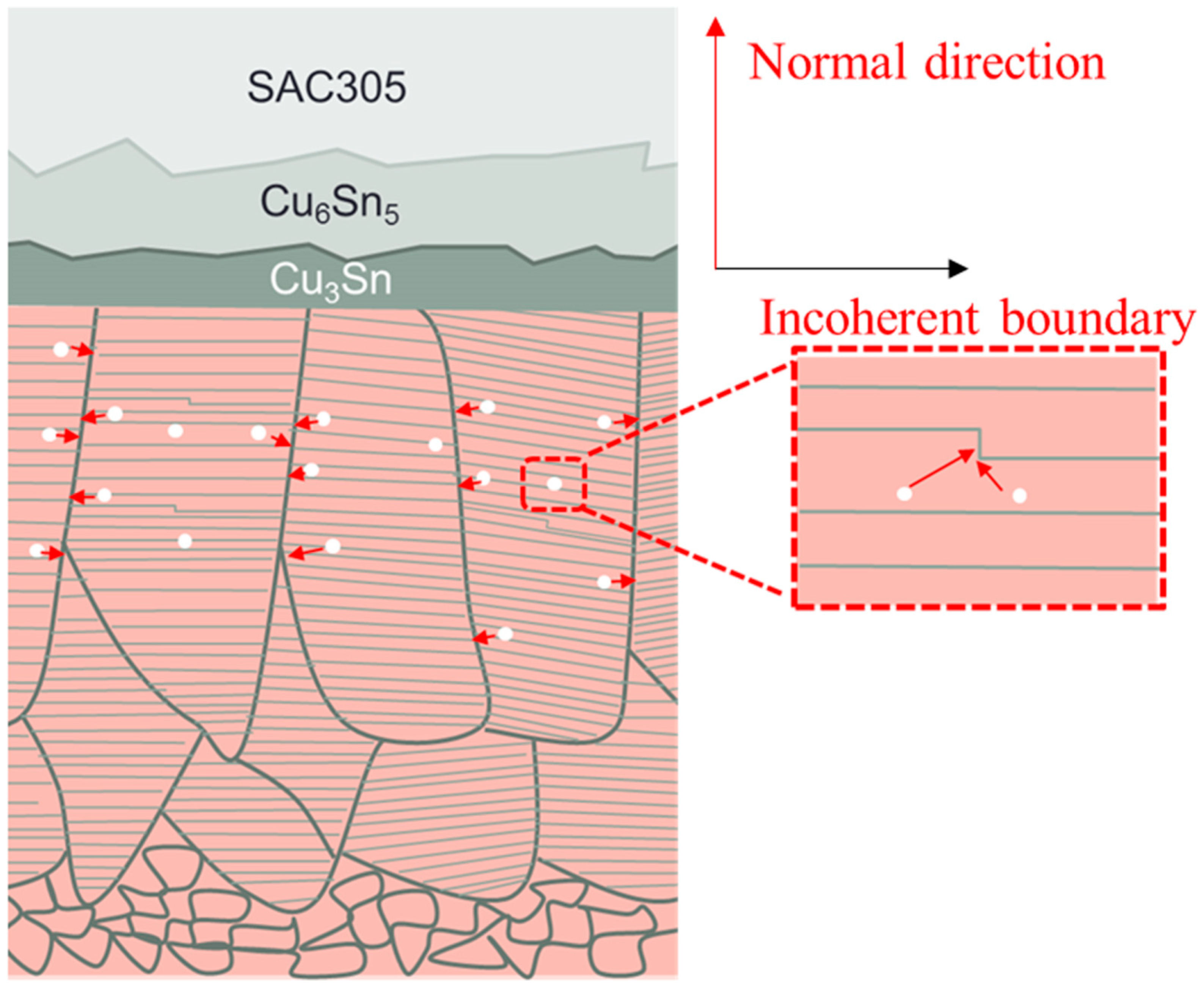
- Zhou, S.; Zhang, Y.B.; Gao, L.Y.; Li, Z.; Liu, Z.Q. The self-healing of Kirkendall voids on the interface between Sn and (111) oriented nanotwinned Cu under thermal aging. Appl. Surf. Sci. 2022, 588, 152900. [Google Scholar] [CrossRef]
- Tsai, S.-T.; Chiang, P.-C.; Liu, C.; Feng, S.-P.; Chen, C.-M. Suppression of Void Formation at Sn/Cu Joint Due to Twin Formation in Cu Electrodeposit. Jom 2019, 71, 3012–3022. [Google Scholar] [CrossRef]
- Lee, H.; Tsai, S.-T.; Wu, P.-H.; Dow, W.-P.; Chen, C.-M. Influence of additives on electroplated copper films and their solder joints. Mater. Charact. 2019, 147, 57–63. [Google Scholar] [CrossRef]
- Tseng, I.-H.; Hsu, Y.-T.; Leu, J.; Tu, K.-N.; Chen, C. Effect of thermal stress on anisotropic grain growth in nano-twinned and un-twinned copper films. Acta Mater. 2021, 206, 116637. [Google Scholar] [CrossRef]
- Hsu, W.-Y.; Tseng, I.-H.; Chiang, C.-Y.; Tu, K.-N.; Chen, C. Distribution of elastic stress as a function of temperature in a 2-μm redistribution line of Cu measured with X-ray nanodiffraction analysis. J. Mater. Res. Technol JMRT 2022, 20, 2799–2808. [Google Scholar] [CrossRef]
- Zhang, Y.-B.; Gao, L.-Y.; Li, X.; Li, Z.; Ma, X.-L.; Liu, Z.-Q.; Sun, R. Electroplating nanotwinned copper for ultrafine pitch redistribution layer (RDL) of advanced packaging technology. In Proceedings of the 2021 22nd International Conference on Electronic Packaging Technology (ICEPT), Xiamen, China, 14–17 September 2021. [Google Scholar] [CrossRef]
- Jin, S.; Wang, G.; Yoo, B. Through-Silicon-Via (TSV) Filling by Electrodeposition of Cu with Pulse Current at Ultra-Short Duty Cycle. J. Electrochem. Soc. 2013, 160, D3300–D3305. [Google Scholar] [CrossRef]
- Kim, Y.; Jin, S.; Park, K.; Lee, J.; Lim, J.-H.; Yoo, B. Effect of Pulse Current and Pre-annealing on Thermal Extrusion of Cu in Through-Silicon via (TSV). Front. Chem. 2020, 8, 771. [Google Scholar] [CrossRef]
- Lin, T.-C.; Liang, C.-L.; Wang, S.-B.; Lin, Y.-S.; Kao, C.-L.; Tarng, D.; Lin, K.-L. Inhibiting the detrimental Cu protrusion in Cu through-silicon-via by highly (111)-oriented nanotwinned Cu. Scr. Mater. 2021, 197, 113782. [Google Scholar] [CrossRef]
- Guo, R.-M.; Xiao, Y.-B.; Gao, Y.; Zhou, S.-Q.; Liu, Y.; Liu, Z.-Q. Interfacial enhancement of Ag and Cu particles sintering using (111)-oriented nanotwinned Cu as substrate for die-attachment. China Welding 2022, 31, 22–28. [Google Scholar]
- Shie, K.-C.; Juang, J.-Y.; Chen, C. Instant Cu-to-Cu direct bonding enabled by 〈111〉-oriented nanotwinned Cu bumps. Jpn. J. Appl. Phys. 2020, 59, SBBA03. [Google Scholar] [CrossRef]
- Ong, J.-J.; Chiu, W.-L.; Lee, O.-H.; Chiang, C.-W.; Chang, H.-H.; Wang, C.-H.; Shie, K.-C.; Yang, S.-C.; Tran, D.-P.; Tu, K.-N.; et al. Low-Temperature Cu/SiO2 Hybrid Bonding with Low Contact Resistance Using (111)-Oriented Cu Surfaces. Materials 2022, 15, 1888. [Google Scholar] [CrossRef]
- Liu, C.-M.; Lin, H.-W.; Huang, Y.-S.; Chu, Y.-C.; Chen, C.; Lyu, D.-R.; Chen, K.-N.; Tu, K.-N. Low-temperature direct copper-to-copper bonding enabled by creep on (111) surfaces of nanotwinned Cu. Sci. Rep. 2015, 5, 9734. [Google Scholar] [CrossRef] [Green Version]
- Shie, K.-C.; Hsu, P.-N.; Li, Y.-J.; Tran, D.-P.; Chen, C. Failure Mechanisms of Cu-Cu Bumps under Thermal Cycling. Materials 2021, 14, 5522. [Google Scholar] [CrossRef]
- Chang, S.-Y.; Chu, Y.-C.; Tu, K.-N.; Chen, C. Effect of anisotropic grain growth on improving the bonding strength of <111>-oriented nanotwinned copper films. Mater. Sci. Eng. A 2021, 804, 140754. [Google Scholar]


| Reference | Electric Field | Environment | VMS | Additives | Nature of nt-Cu |
|---|---|---|---|---|---|
| Lei. Lu [11] | PED: ton = 0.02 s; toff = 2 s; Jpeak = 0.5 A/cm2 | pH~1 20 ± 1 °C | CuSO4 | / | Film: The average grain size was about 400 nm and contained a high density of growth twins of the {111}/[112] type. |
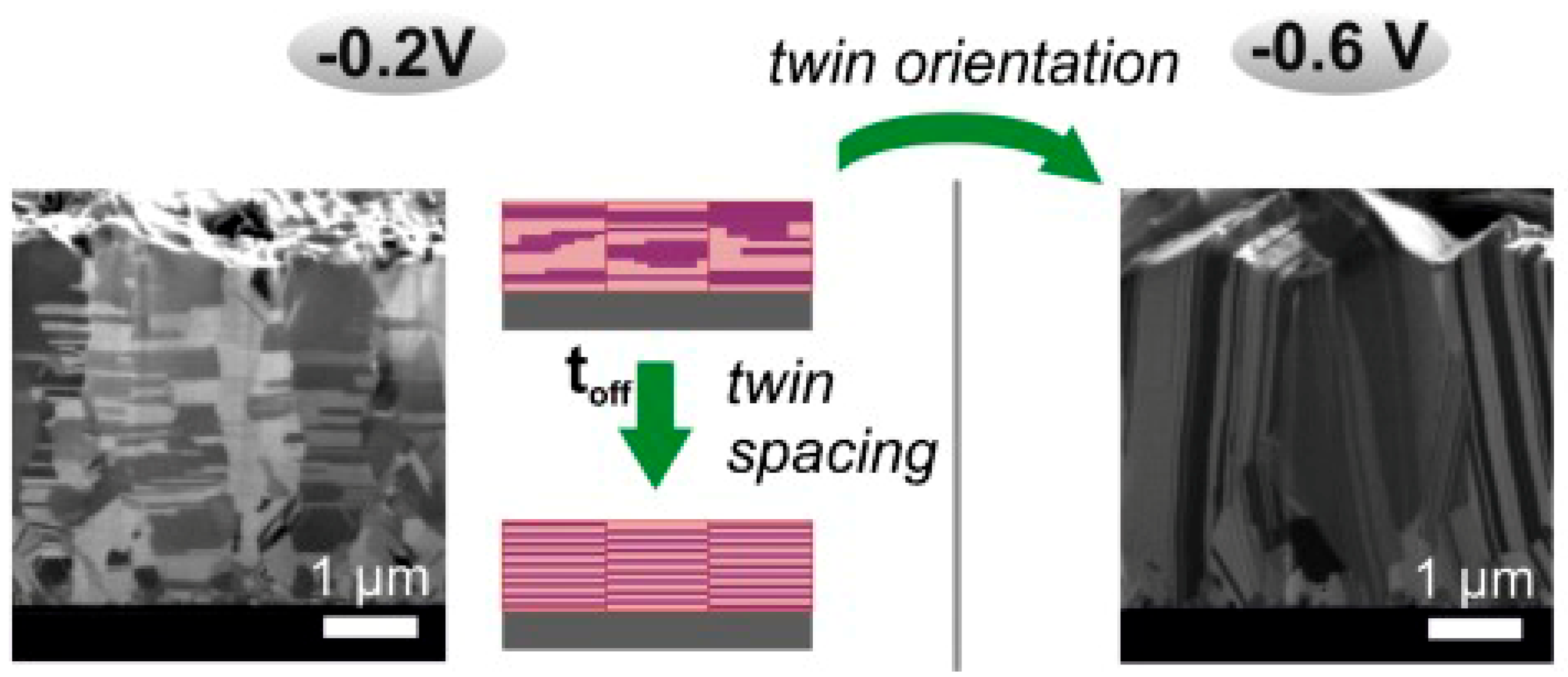
| Madoka Hasegawa [59] | PED: −0.2 V or −0.6 V vs. SCE; ton = 0.02 s; toff = 1–4 s | standard three-electrode cell with a Pt mesh and a saturated calomel electrode | 65 g/L CuSO4· 5H2O 1196 g/L H2SO4 50 mg/L HCl | 100 mg/L polyethylene glycol (Mw 4000) 10 mg/L 3-Mercapto-1-propanesulfonic acid sodium salt | Film: Horizontal nt-Cu obtained at −0.2 V vs. SCE, and twin spacing reduced with increasing toff; vertical nt-Cu obtained at −0.6 V vs. SCE. |
| Gong Cheng [77] | PED: Jpeak = 100 mA/cm2; frequency = 2.5 Hz; Javg = 1 ASD | pH = 1 | 80 g/L CuSO4 50 ppm Cl− | / | Film: The average grain diameter was about 1.93 μm. The average twin lamella thickness was about 116.2 nm. |
| Xiaodei Zhan [52] | PED: Javg = 2 ASD; γ = 30% | Stirring rate: 800 rpm | 15–125 g/L CuSO4· 5H2O 184 g/L H2SO4 10 ppm Cl− | / | Film: Twin thickness decrease with increase in the pulse frequency; a spiral feature of a hexagonal pyramid was found on the top of nt-Cu. |
| Mengya Dong [78] | PED: Jpeak = 4 A/cm2; ton = 20 ms; toff = 1 s; 2000 cycles | pH = 1 25 °C | 1.0 M CuSO4 NaCl | / | Cu micro-cone arrays with densely packed vertical nanotwins. |
| Gong Cheng [79] | PED: ton = 4 ms; toff = 196 ms; Javg = 2 ASD | pH = 1 | CuSO4 80 g/L 50 ppm Cl− | / | RDL: The thickness of Cu foils was about 7 μm. The clear twin lamellae averaged 116.2 nm and were perpendicular to the film surface. |
| Sanghyun Jin [80] | PED: Jpeak = 50–200 mA/cm2; ton = 0.02 s; toff = 0.65 s | pH = 0.8 | 0.8 M CuSO4 50 ppm HCl | 1 mL/L S-Additive A (Samsung Electronics Co.) 5 mL/L S-Additive B (Samsung Electronics Co.) | TSV: The aspect ratio of via was 9.17 (diameter = 6 μm, depth = 55 μm; v-shaped TSV filling; win spacing was about several tens of nanometers. |
| Yu-Xi Wang [67] | PED: Jpeak = 60 ASD; ton = 0.02 s; toff = 0.5–4 s | Stirring rate: 300 rpm 25 ± 1 °C | 50–100 g/L CuSO4· 5H2O H2SO4 50 ppm Cl− | PEG 0–40 ppm MPS | Damascene via: The via was about 1.4 μm deep,1.4 μm wide at the bottom, and 1.9 μm wide at the top; the aspect ratio was about 1:1. |
| Kuan-Ju Chen [44] | Periodic-reverse (PR) wave forms: Jpeak/Jzvg = 8/8 or 8/4 ASD; ton/trev = 40/1–40/6 | / | 196 g/L CuSO4 40 ppm Cl− | 4 mL/L organic additive | Film: Highly <111>-oriented columnar nt-Cu with thin transition layers. |
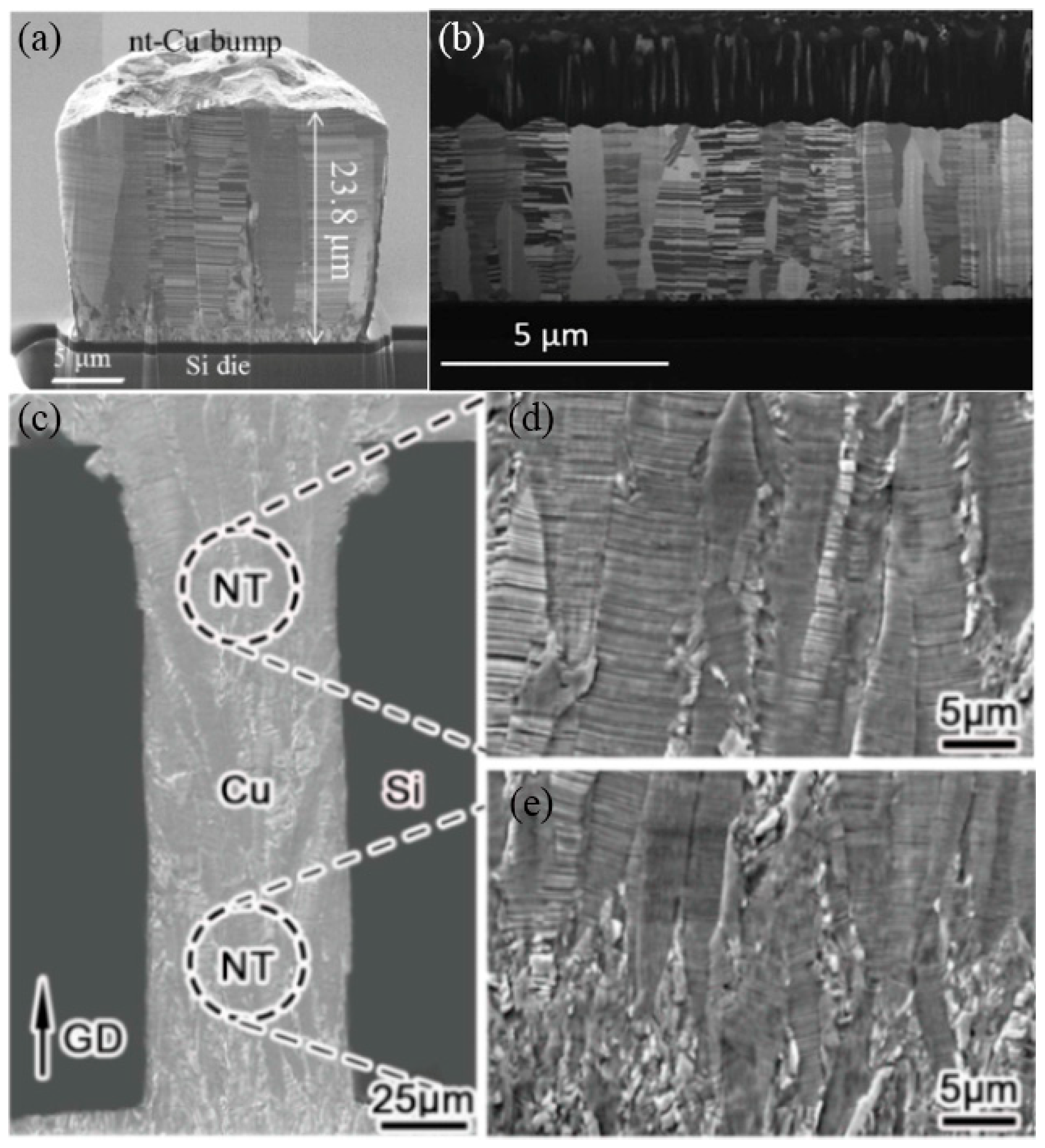
| I-Hsin Tseng [26] | Periodic-reverse electroplating: Jon-time = 4 ASD, ton = 40 ms Joff-time = −1 ASD, toff = 4 ms | / | 0.8 M Cu2+ in CuSO4 40 ppm HCl 100 g/L H2SO4 | additives | RDL: The length was 800 μm, the height was 5 μm, and the width was 10 μm with a denser nt-Cu with a thin area of fine grain at the bottom. |
| K. N. Tu’s group [72,81,82,83] | Aspect-ratio-dependent electroplating 30 h | / | Cu 40 g/L Sulfuric acid 150 g/L Chloride 50 mg/L | Leveler 15 mL/L Brightener 10 mL/L | Through-wafer Cu interconnection: Twin lamellar width was ~20 nm. |
| Hsuan Lee [84] | DC: 0.34 ASD | 28 °C | 0.88 M CuSO4· 5H2O 0.54 M H2SO4 60 ppm NaCl | PEG (8000 g/mol) | Film: Slender columnar nanotwins with Σ3 TBs (60° rotation at <111>) perpendicular to the substrate. |
| Chih-Han Tseng [64] | DC: 5–11 ASD 8 min | Stirring rate: 1200 rpm | 0.8 M Cu2+ 50–110 g/L H2SO4 80 ppm Cl− | 4000 ppm ECD-107A | Film: (111)-oriented columnar nt-Cu grains. Twin thickness increased with current density. |
| Chun-Cheng Lin [85] | DC: 400 mA/cm2 | 12 ± 0.2 °C | 1.08 M CuSO4· 5H2O 25 mM H2SO4 0.7 mM NaCl | 60–300 ppm MPS | Film: Thickness of twin lamella ranged from 10–240 nm; large columnar grains composed of highly ordered twin lamellae with a v-shaped grain boundary. |
| Yu Bai [61] | DC: 1–5 ASD | Stirring rate: 200 rpm | 195 g/L CuSO4· 5H2O 13 mL/L H2SO4 40 ppm NaCl | commercial additive | Film: Vertical nt-Cu with a (220) texture. |
| Fu-Long Sun [66] | DC: 30 mA/cm2 | Stirring rate: 300 rpm | 0.8 mol/L Cu2+ 3–17 mL/L H2SO4 40 ppm NaCl | organic additive | Film: Equiaxed crystals of small size (grain size of about 100 nm) near the bottom substrate, columnar twin-free grains in the middle (lateral size of about 6.8 μm), and columnar nanotwinned grains near the top surface (lateral size of about 7.9 μm). |
| K. N. Tu’ group [24,86,87] | DC: 40–100 mA/cm2 | Stirring rate: 1200 rpm | CuSO4 solution 40 ppm HCl | surfactants | CuP: Densely-packed (111) nanotwins aligned vertically in the growth direction. |
| Hsiang-Yao Hsiao [21] | DC: 80 mA/cm2 | Stirring rate: 600–1200 rpm | CuSO4 40 ppm HCl | proper surfactants | UBM: 20 μm thick (111)-oriented columnar nt-Cu. |
| Tao-Chi Liu [60] | DC: 20–70 mA/cm2 | Stirring rate: 400–1500 rpm | 0.8 M Cu2+ in CuSO4 solution with 40 ppm HCl | surfactants | UBM: 20 μm thick Cu pad with a 100 μm diameter; the columnar grains were [111]-riented. The average grain size was 3.4 ± 0.7 μm. |
| Jing Huang [71] | DC: 30 mA/cm2 | Stirring rate: 300–900 rpm 25 ± 2 °C | 120–200 g/L CuSO4· 5H2O 3–80 mL/L H2SO4 30–100 ppm NaCl | 0–100 ppm gelatin 0–20 ppm SH110 | RDL: The width and pitch of the RDLs were both 15 μm; equiaxed fine grains near the seed layer and columnar grains at the top of the RDLs. |
| Fu-Long Sun [25] | DC: 30 mA/cm2 | Stirring rate: 300 rpm | 75 g/L CuSO4 3 mg/L H2SO4 | 5–70 mg/L gelatin | TSV: Diameter of 30~50 μm and aspect ratio of ~4. The average twin thickness was about 22 nm. |
Disclaimer/Publisher’s Note: The statements, opinions and data contained in all publications are solely those of the individual author(s) and contributor(s) and not of MDPI and/or the editor(s). MDPI and/or the editor(s) disclaim responsibility for any injury to people or property resulting from any ideas, methods, instructions or products referred to in the content. |
© 2023 by the authors. Licensee MDPI, Basel, Switzerland. This article is an open access article distributed under the terms and conditions of the Creative Commons Attribution (CC BY) license (https://creativecommons.org/licenses/by/4.0/).
Share and Cite
Chen, K.-X.; Gao, L.-Y.; Li, Z.; Sun, R.; Liu, Z.-Q. Research Progress of Electroplated Nanotwinned Copper in Microelectronic Packaging. Materials 2023, 16, 4614. https://doi.org/10.3390/ma16134614
Chen K-X, Gao L-Y, Li Z, Sun R, Liu Z-Q. Research Progress of Electroplated Nanotwinned Copper in Microelectronic Packaging. Materials. 2023; 16(13):4614. https://doi.org/10.3390/ma16134614
Chicago/Turabian StyleChen, Ke-Xin, Li-Yin Gao, Zhe Li, Rong Sun, and Zhi-Quan Liu. 2023. "Research Progress of Electroplated Nanotwinned Copper in Microelectronic Packaging" Materials 16, no. 13: 4614. https://doi.org/10.3390/ma16134614
APA StyleChen, K.-X., Gao, L.-Y., Li, Z., Sun, R., & Liu, Z.-Q. (2023). Research Progress of Electroplated Nanotwinned Copper in Microelectronic Packaging. Materials, 16(13), 4614. https://doi.org/10.3390/ma16134614