
Luminescence Properties of Epitaxial Cu2O Thin Films Electrodeposited on Metallic Substrates and Cu2O Single Crystals

 ,
,
Abstract
1. Introduction
2. Materials and Methods
3. Results
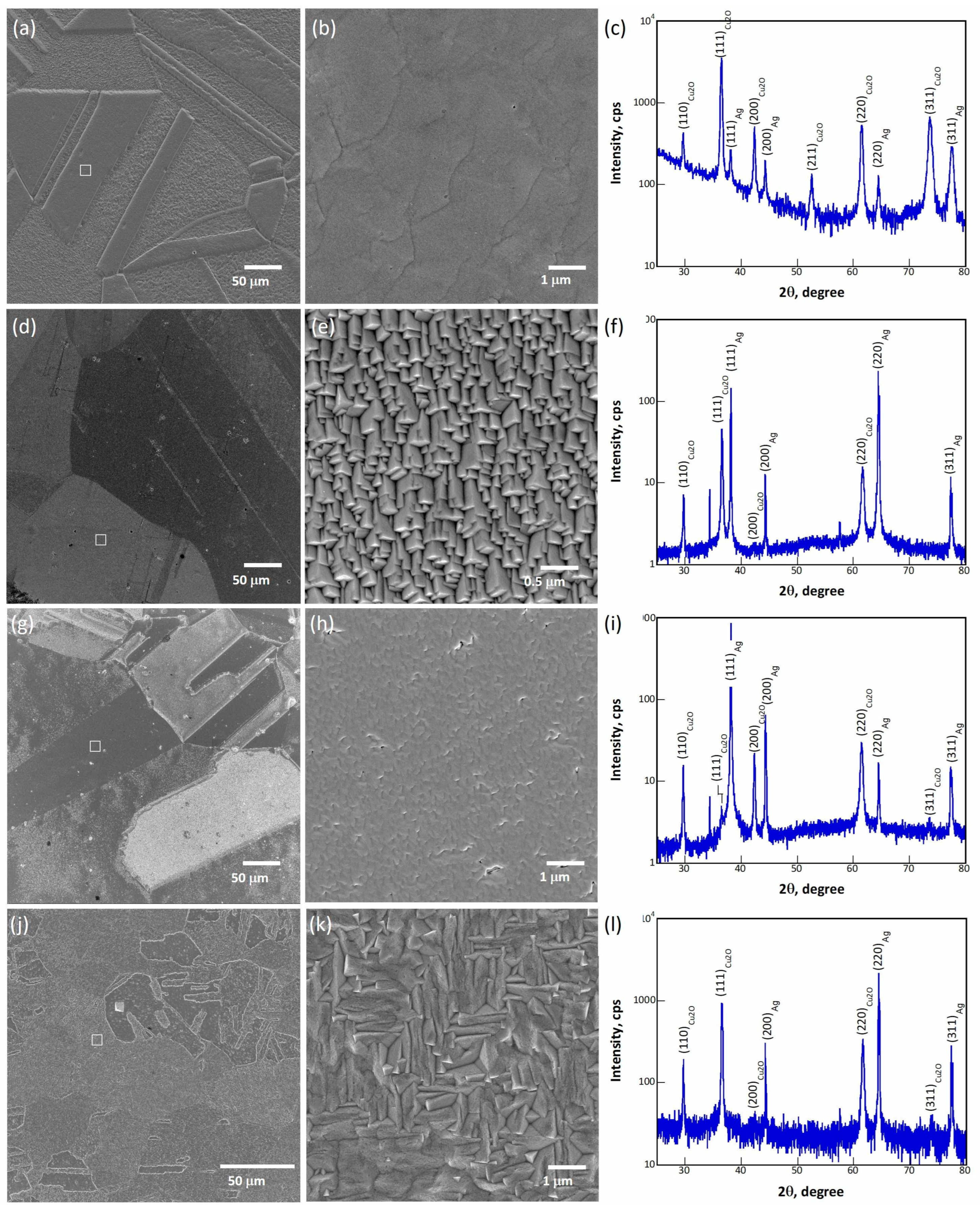
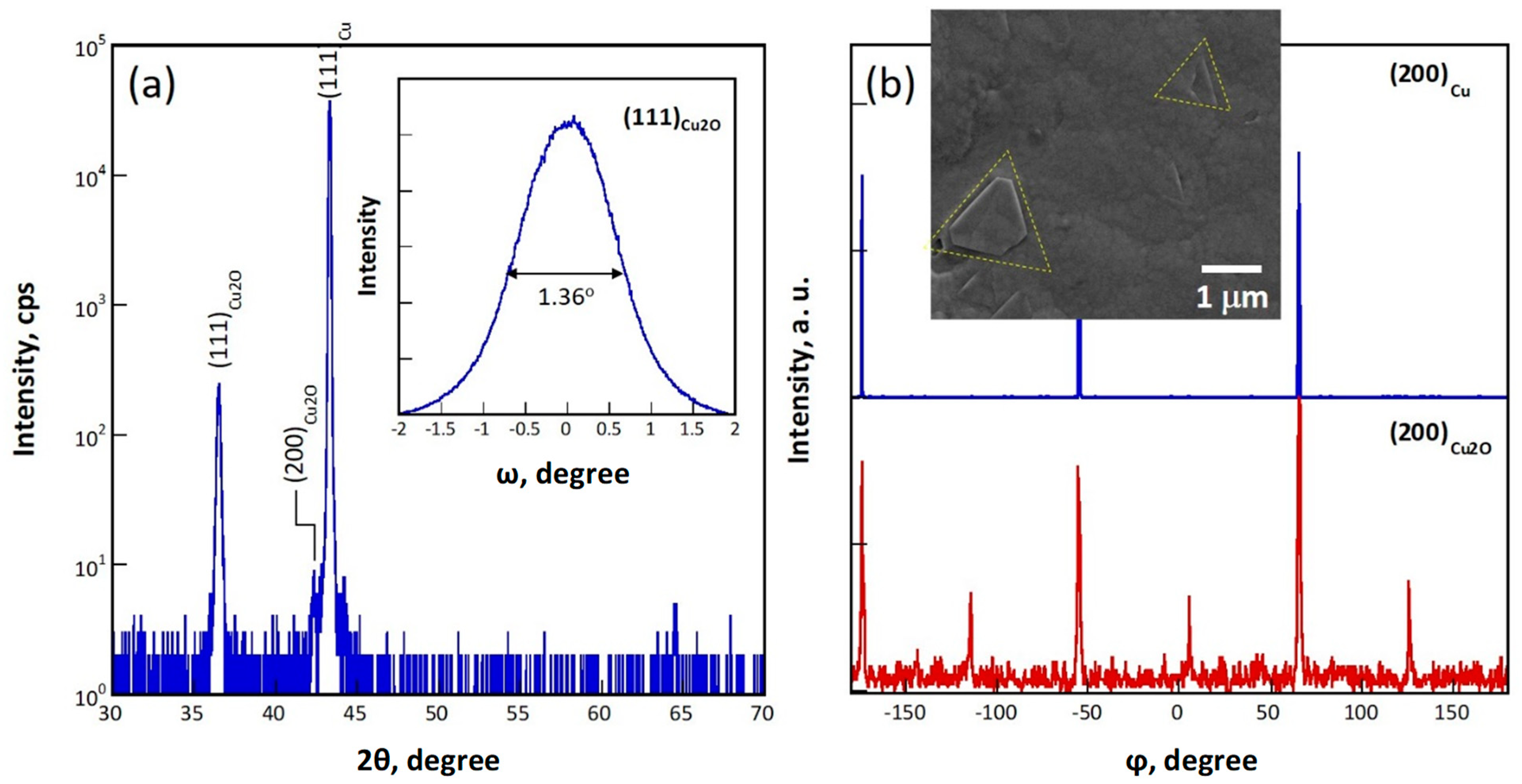
3.1. Microstructure
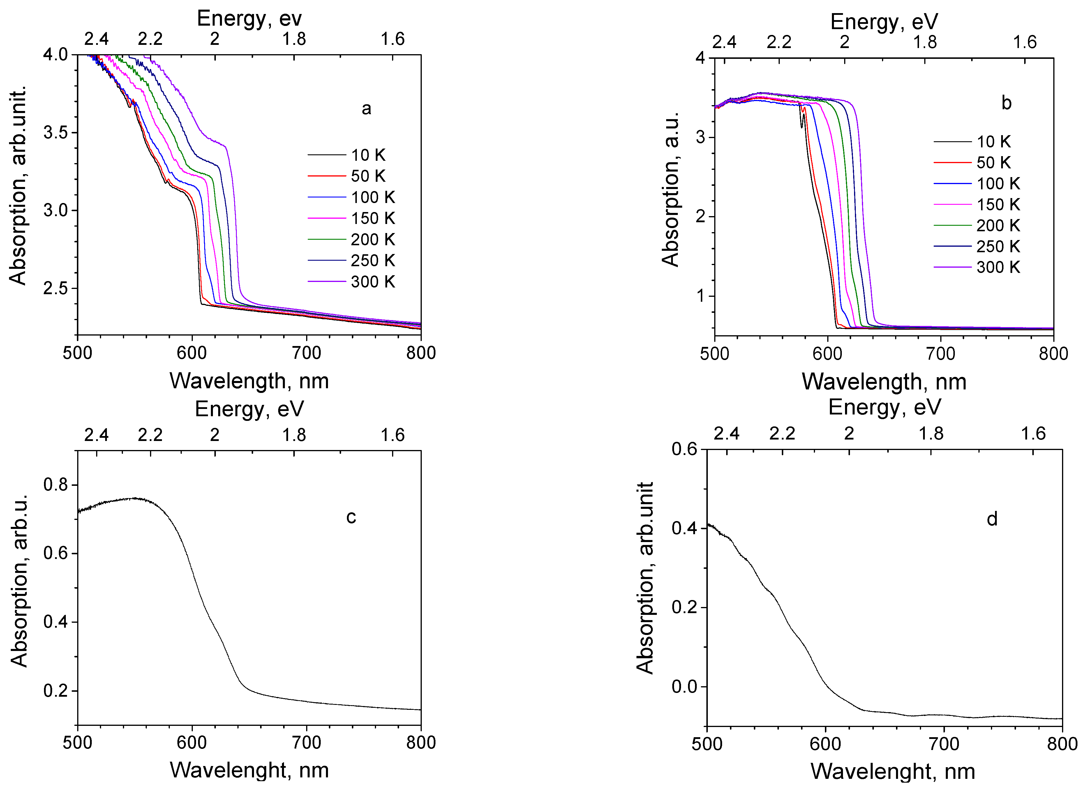
3.2. Absorption
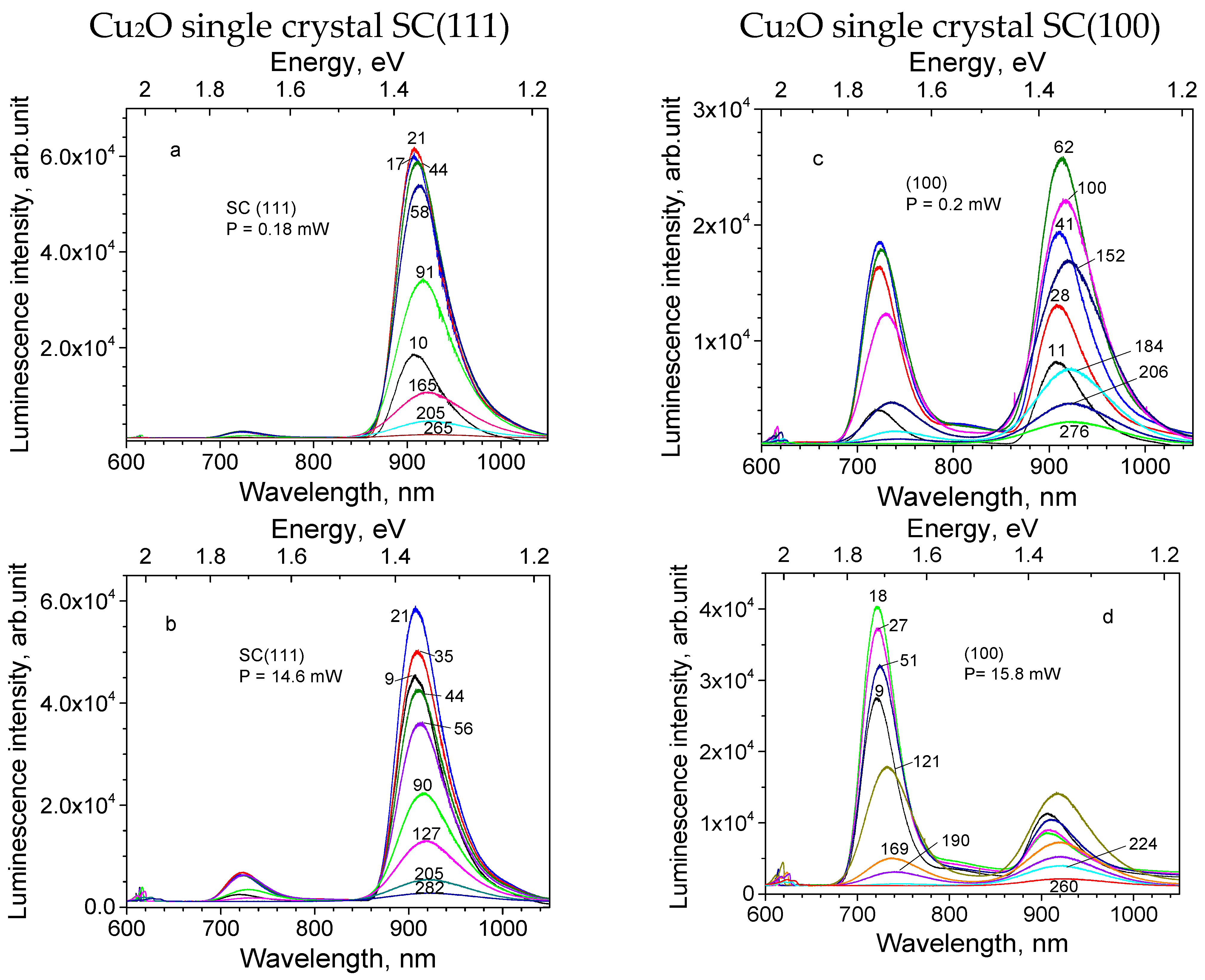
3.3. Photoluminescence
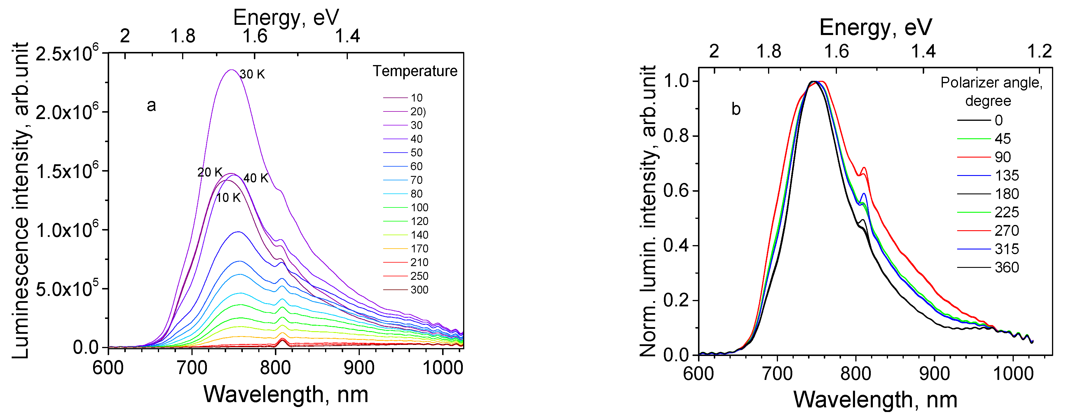
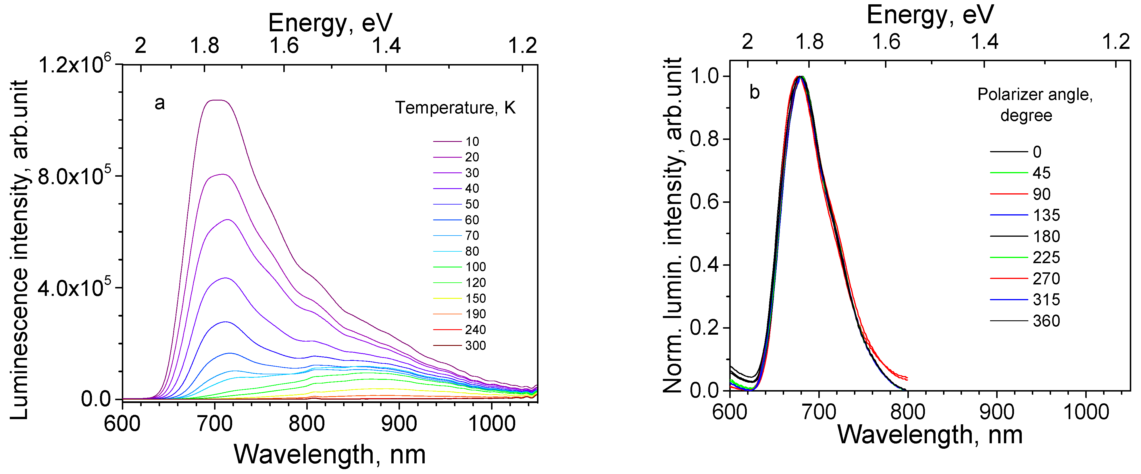
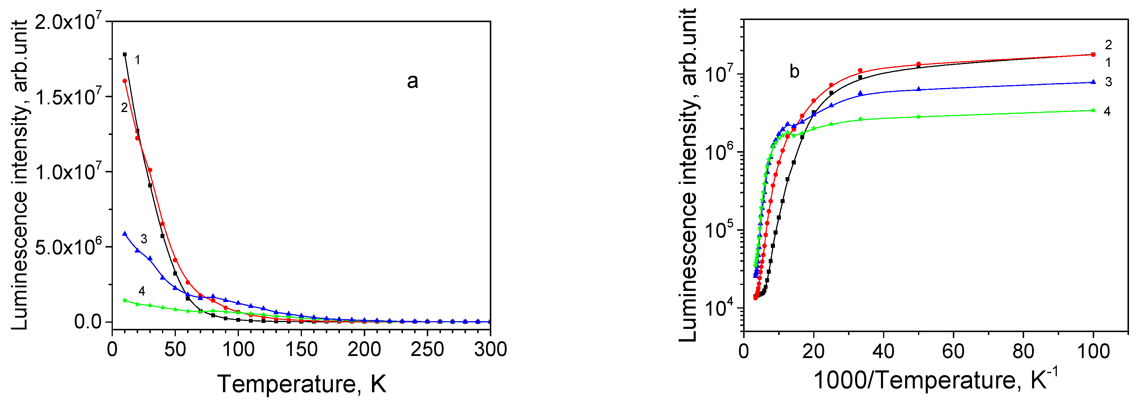
3.3.1. Cu2O Single Crystals
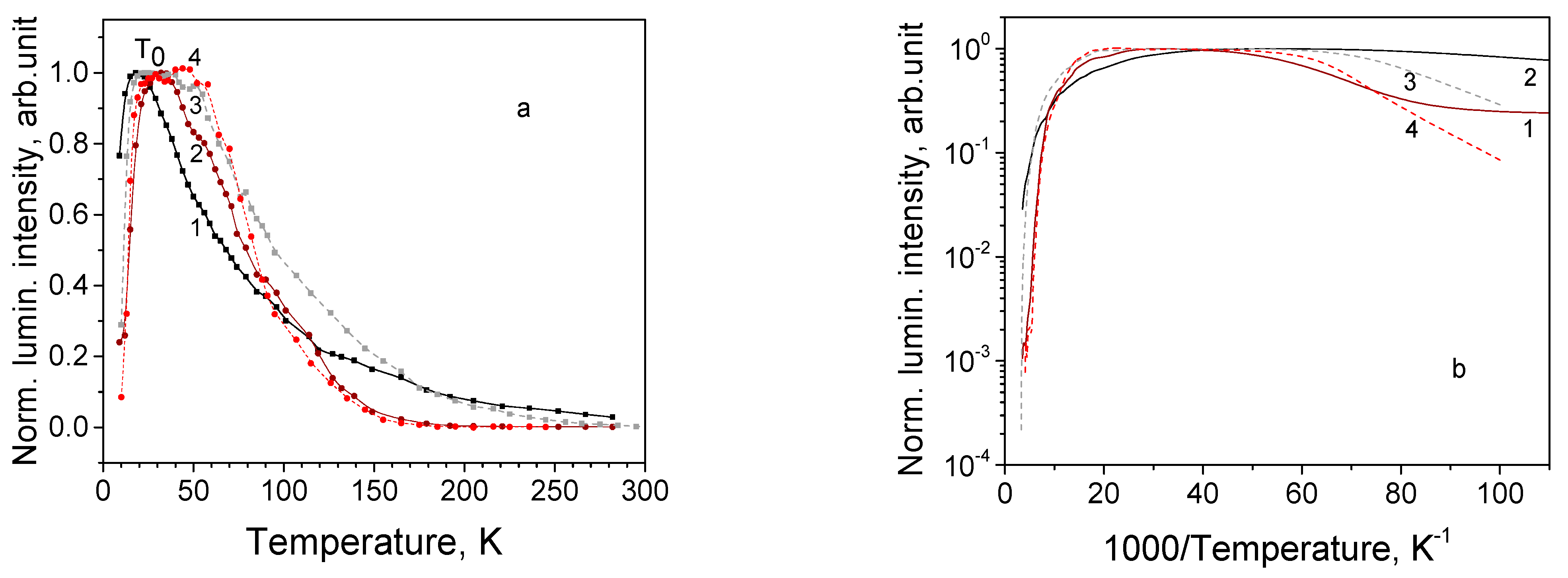
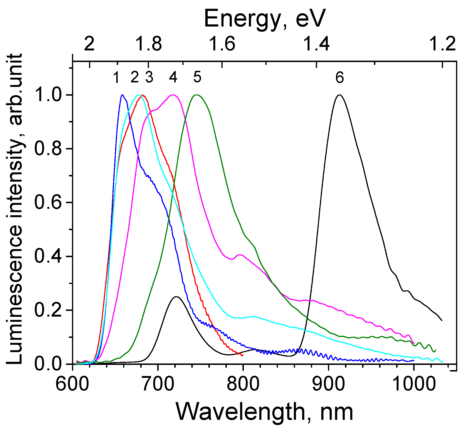
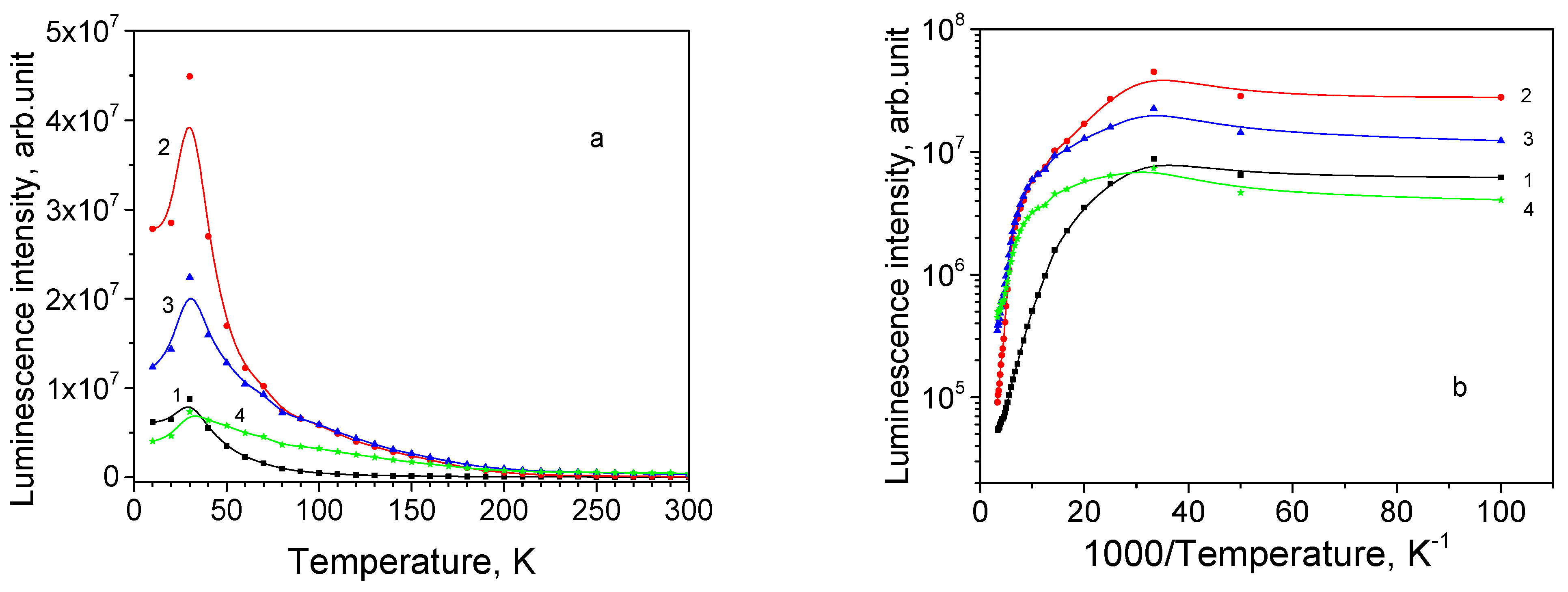
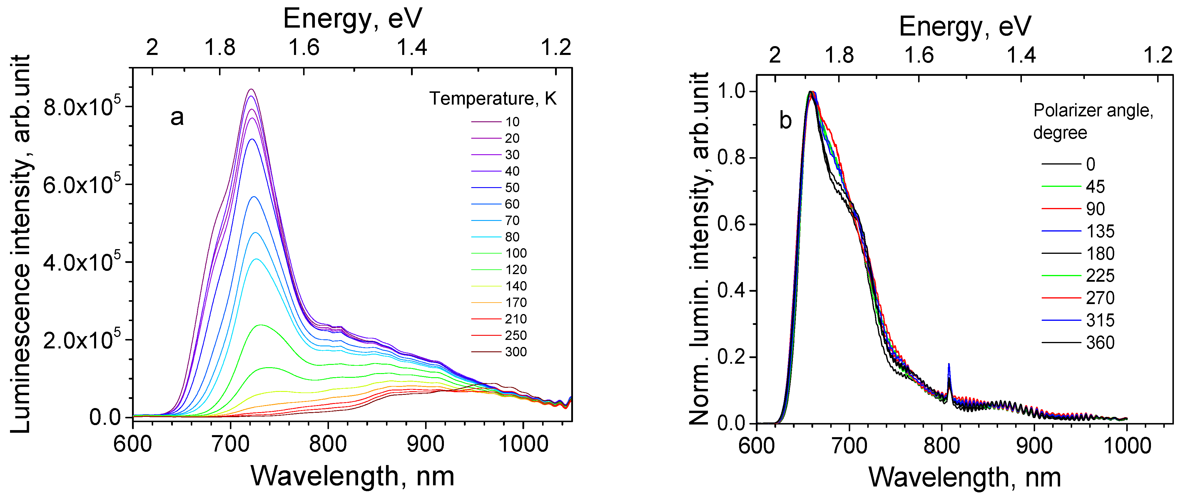
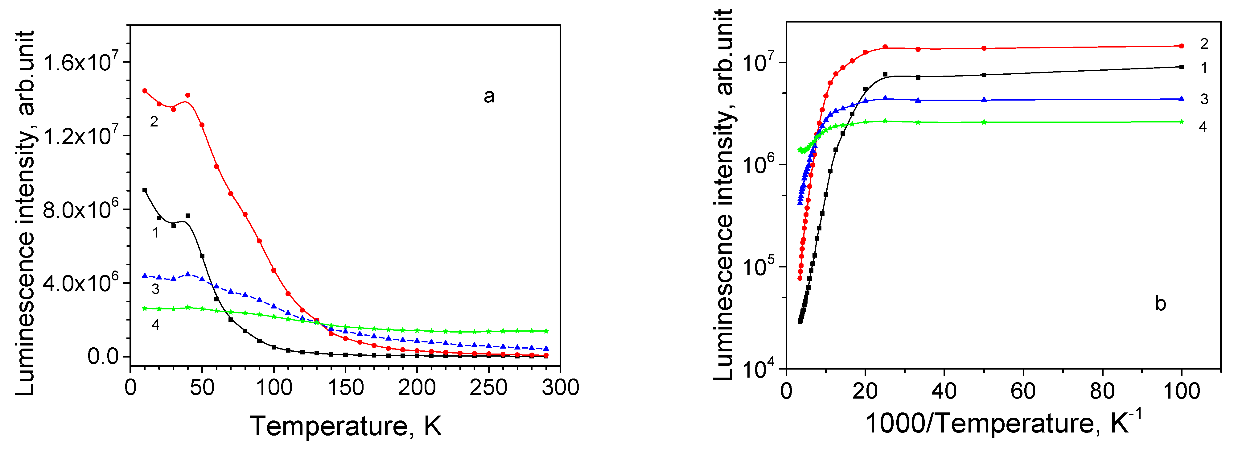
3.3.2. Cu2O Thin Films
4. Discussion
4.1. Absorption
4.2. Photoluminescence
4.2.1. Single Crystals
4.2.2. Thin Films
5. Conclusions
Supplementary Materials
Author Contributions
Funding
Institutional Review Board Statement
Informed Consent Statement
Data Availability Statement
Conflicts of Interest
References
- Joint Committee on Powder Diffraction Standards. American Society for Testing and Materials Selected Powder Diffraction Data for Minerals: Data Book; Set 1-5 (Revised), File 5-0667; Joint Committee on Powder Diffraction Standards: Pennsylvania, PA, USA, 1974; p. 664. [Google Scholar]
- Raebiger, H.; Lany, S.; Zunger, A. Origins of the p-type nature and cation deficiency in Cu2O and related materials. Phys. Rev. B 2007, 76, 045209. [Google Scholar] [CrossRef]
- Han, S.; Flewitt, A.J. Analysis of the conduction mechanism and copper vacancy density in p-type Cu2O thin films. Sci. Rep. 2017, 7, 5766. [Google Scholar] [CrossRef] [PubMed]
- Hayashi, M.; Katsuki, K. Hydrogen-Like Absorption Spectrum of Cuprous Oxide. J. Phys. Soc. Jpn. 1952, 7, 599–603. [Google Scholar] [CrossRef]
- Li, J.; Mei, Z.; Ye, D.; Liang, H.; Liu, L.; Liu, Y.; Galeckas, A.; Kuznetsov, A.Y.; Du, X. Engineering of optically defect free Cu2O enabling exciton luminescence at room temperature. Opt. Mater. Express 2013, 3, 2072–2077. [Google Scholar] [CrossRef]
- Ito, T.; Masumi, T. Detailed examination of relaxation processes of excitons in photoluminescence spectra of Cu2O. J. Phys. Soc. Jpn. 1997, 66, 2185–2193. [Google Scholar] [CrossRef]
- Kazimierczuk, T.; Fröhlich, D.; Scheel, S.; Stolz, H.; Bayer, M. Giant Rydberg excitons in the copper oxide Cu2O. Nature 2014, 514, 343–347. [Google Scholar] [CrossRef]
- Versteegh, M.A.M.; Steinhauer, S.; Bajo, J.; Lettner, T.; Soro, A.; Romanova, A.; Gyger, S.; Schweickert, L.; Mysyrowicz, A.; Zwiller, V. Giant Rydberg excitons in Cu2O probed by photoluminescence excitation spectroscopy. Phys. Rev. B 2021, 104, 245206. [Google Scholar] [CrossRef]
- Trinkler, L.; Aulika, I.; Krieke, G.; Nilova, D.; Ruska, R.; Butikova, J.; Berzina, B.; Chou, M.M.-C.; Chang, L.; Wen, M.-C.; et al. Characterization of wurtzite Zn1−xMgxO epilayers grown on ScAlMgO4 substrate by methods of optical spectroscopy. J. Alloys Compd. 2022, 912, 165178. [Google Scholar] [CrossRef]
- Li, J.; Mei, Z.; Liu, L.; Liang, H.; Azarov, A.; Kuznetsov, A.; Liu, Y.; Ji, A.; Meng, Q.; Du, X. Probing defects in nitrogen-doped Cu2O. Sci. Rep. 2014, 4, 7240. [Google Scholar] [CrossRef]
- Sun, S.; Zhang, X.; Yang, Q.; Liang, S.; Zhang, X.; Yang, Z. Cuprous oxide (Cu2O) crystals with tailored architectures: A comprehensive review on synthesis, fundamental properties, functional modification and applications. Prog. Mater. Sci. 2018, 96, 111–173. [Google Scholar] [CrossRef]
- Zoolfakar, A.S.; Rani, R.A.; Morfa, A.J.; O’Mullane, A.P.; Kalantar-Zadeh, K. Nanostructured copper oxide semiconductors: A perspective on materials, synthesis methods and applications. J. Mater. Chem. C 2014, 2, 5247–5270. [Google Scholar] [CrossRef]
- Brandt, I.S.; Tumelero, M.A.; Pelegrini, S.; Zangari, G.; Pasa, A.A. Electrodeposition of Cu2O: Growth, properties, and applications. J. Solid State Electrochem. 2017, 21, 1999–2020. [Google Scholar] [CrossRef]
- Murali, D.S.; Kumar, S.; Choudhary, R.J.; Wadikar, A.D.; Jain, M.K.; Subrahmanyam, A. Synthesis of Cu2O from CuO thin films: Optical and electrical properties. AIP Adv. 2015, 5, 047143. [Google Scholar] [CrossRef]
- Wong, T.K.S.; Zhuk, S.; Masudy-Panah, S.; Dalapati, G.K. Current status and future prospects of copper oxide heterojunction solar cells. Materials 2016, 9, 271. [Google Scholar] [CrossRef]
- Al-Jawhari, H.A. A review of recent advances in transparent p-type Cu2O-based thin film transistors. Mater. Sci. Semicond. Process. 2015, 40, 241–252. [Google Scholar] [CrossRef]
- Chen, L.C. Review of preparation and optoelectronic characteristics of Cu2O-based solar cells with nanostructure. Mater. Sci. Semicond. Process. 2013, 16, 1172–1185. [Google Scholar] [CrossRef]
- Yeh, H.H.; Wen, M.C.; Chang, L.; Ploog, K.H.; Chou, M.M.C. Epitaxial growth of Cu2O on Cu substrate—A combinatorial substrate approach. J. Cryst. Growth 2019, 512, 124–130. [Google Scholar] [CrossRef]
- Kobayashi, H.; Nakamura, T.; Takahashi, N. Preparation of Cu2O films on MgO (1 1 0) substrate by means of halide chemical vapor deposition under atmospheric pressure. Mater. Chem. Phys. 2007, 106, 292–295. [Google Scholar] [CrossRef]
- Wang, Y.; Ghanbaja, J.; Soldera, F.; Boulet, P.; Horwat, D.; Mücklich, F.; Pierson, J.F. Controlling the preferred orientation in sputter-deposited Cu2O thin films: Influence of the initial growth stage and homoepitaxial growth mechanism. Acta Mater. 2014, 76, 207–212. [Google Scholar] [CrossRef]
- Liu, X.; Xu, M.; Zhang, X.; Wang, W.; Feng, X.; Song, A. Pulsed-laser-deposited, single-crystalline Cu2O films with low resistivity achieved through manipulating the oxygen pressure. Appl. Surf. Sci. 2018, 435, 305–311. [Google Scholar] [CrossRef]
- Ha, T.; Park, I.; Sim, K.I.; Lee, H.; Bae, J.-S.; Kim, S.J.; Kim, J.P.; Kim, T.-T.; Kim, J.H.; Jang, J.I.; et al. Single-crystalline Cu2O thin films of optical quality as obtained by the oxidation of single-crystal Cu thin films at low temperature. APL Mater. 2019, 7, 031115. [Google Scholar] [CrossRef]
- Elmahdy, M.M.; El-Shaer, A. Structural, optical and dielectric investigations of electrodeposited p-type Cu2O. J. Mater. Sci. Mater. Electron. 2019, 30, 19894–19905. [Google Scholar] [CrossRef]
- Izaki, M.; Sasaki, S.; Mohamad, F.B.; Shinagawa, T.; Ohta, T.; Watase, S.; Sasano, J. Effects of preparation temperature on optical and electrical characteristics of (111)-oriented Cu2O films electrodeposited on (111)-Au film. Thin Solid Films 2012, 520, 1779–1783. [Google Scholar] [CrossRef]
- Liu, Y.L.; Mu, R.; Yang, H.; Shao, C.L.; Zhang, J.Y.; Lu, Y.M.; Shen, D.Z.; Fan, X.W. The structural and optical properties of Cu2O films electrodeposited on different substrates. Semicond. Sci. Technol. 2005, 20, 44–50. [Google Scholar] [CrossRef]
- Gloystein, A.; Nilius, N. Luminescence from cuprous oxide in a scanning tunneling microscope: Competition between plasmonic and excitonic response. ACS Photonics 2022, 9, 3625–3632. [Google Scholar] [CrossRef]
- Ravichandiran, C.; Sakthivelu, A.; Davidprabu, R.; Valanarasu, S.; Kathalingam, A.; Ganesh, V.; Shkir, M.; Algarni, H.; AlFaify, S. In-depth study on structural, optical, photoluminescence and electrical properties of electrodeposited Cu2O thin films for optoelectronics: An effect of solution pH. Microelectron. Eng. 2019, 210, 27–34. [Google Scholar] [CrossRef]
- Frazer, L.; Chang, K.B.; Schaller, R.D.; Poeppelmeier, K.R.; Ketterson, J.B. Vacancy relaxation in cuprous oxide (Cu2−xO1−y). J. Lumin. 2017, 183, 281–290. [Google Scholar] [CrossRef]
- Bohannan, E.W.; Shumsky, M.G.; Switzer, J.A. Epitaxial electrodeposition of copper (I) oxide on single-crystal gold(100). Chem. Mater. 1999, 11, 2289–2291. [Google Scholar] [CrossRef]
- Dai, D.; Huang, P.-Y.; Wu, T.-Y.; Shih, C.-H. Chang Epitaxial electrodeposition of Cu2O on Ag substrates in sulfate baths. J. Cryst. Growth 2023, 603, 126983. [Google Scholar] [CrossRef]
- Kaufman, R.G.; Hawkins, R.T. Defect Luminescence of Thin Films of Cu2O on Copper. J. Electrochem. Soc. 1984, 131, 385. [Google Scholar] [CrossRef]
- Duvvury, C.; Kenway, D.J.; Weichman, F.L. Excitation characteristics of the IR luminescence in Cu2O. J. Lumin. 1975, 10, 415. [Google Scholar] [CrossRef]
- Solache-Carranco, H.; Juárez-Díaz, G.; Esparza-García, A.; Briseño-García, M.; Galván-Arellano, M.; Martínez-Juárez, J.; Romero-Paredes, G.; Peña-Sierra, R. Romero-Paredes, and R. Pena-Sierra, Photoluminescence and X-ray diffraction studies on Cu2O. J. Lumin. 2009, 129, 1483. [Google Scholar] [CrossRef]
- Sun, S.; He, L.; Yang, M.; Cui, J.; Liang, S. Facet junction engineering for photocatalysis: A comprehensive review on elementary knowledge, facet-synergistic mechanisms, functional modifications, and future perspectives. Adv. Funct. Mater. 2022, 32, 2106982. [Google Scholar] [CrossRef]
- Li, Y.; Wang, Z.; Tao, R.; Fan, Y.; Xu, J.; Yu, L.; Ren, N.; Wu, J.; Chen, D.; Shao, Z. Preparation strategies of p-type cuprous oxide and its solar energy conversion performance. Adv. Funct. Mater. 2020, 30, 2002606. [Google Scholar] [CrossRef]
- Tan, C.-S.; Hsu, S.-C.; Ke, W.-H.; Chen, L.-J.; Huang, M.H. Facet-dependent electrical conductivity properties of Cu2O crystals. Nano Lett. 2015, 15, 2155–2160. [Google Scholar] [CrossRef]
- Dai, D.; Yao, W.-T.; Yan, T.; Chang, L. Effect of electrolyte concentration on the epitaxial growth of ZnO on Cu substrate in electrochemical deposition. J. Electrochem. Soc. 2020, 167, 162505. [Google Scholar] [CrossRef]
- Baker, S.P.; Hoffman, B.; Timian, L.; Silvernail, A.; Ellis, E.A. Texture transformations in Ag thin films. Acta Mater. 2013, 61, 7121–7132. [Google Scholar] [CrossRef]
- Williamson, G.K.; Hall, W.H. X-ray line broadening from filed aluminium and wolfram. Acta Metall. 1953, 1, 22–31. [Google Scholar] [CrossRef]
- Kracht, M.; Schörmann, J.; Eickhoff, M. Plasma assisted molecular beam epitaxy of Cu2O on MgO(001): Influence of copper flux on epitaxial orientation. J. Cryst. Growth 2016, 436, 87–91. [Google Scholar] [CrossRef]
- Dhanabalan, K.; Ravichandran, A.T.; Ravichandran, K.; Valanarasu, S.; Mantha, S. Effect of Co doped material on the structural, optical and magnetic properties of Cu2O thin films by SILAR technique. J. Mater. Sci. Mater. Electron. 2017, 28, 4431–4439. [Google Scholar] [CrossRef]
- Meyer, B.K.; Polity, A.; Reppin, D.; Becker, M.; Hering, P.; Klar, P.J.; Sander, T.; Reindl, C.; Benz, J.; Eickhoff, M.; et al. Binary copper oxide semiconductors: From materials towards devices. Phys. Stat. Sol. B 2012, 249, 1487–1509. [Google Scholar] [CrossRef]
- Cakir, D. Enhanced Raman Signatures on Copper-Based Materials. Ph.D. Thesis, Universite Montpelier, Montpelier, France, 2017. (In English). [Google Scholar]
- Ito, T.; Yamaguchi, H.; Okabe, K.; Masumi, T. Single crystal growth and characterization of Cu2O and CuO. J. Mater. Sci. 1998, 33, 3555–3566. Available online: https://rdcu.be/c9o9D (accessed on 15 January 2023). [CrossRef]
- Steinhauer, S.; Versteegh, M.A.M.; Gyger, S.; Elshaari, A.W.; Kunert, B.; Mysyrowicz, A.; Zwiller, V. Rydberg excitons in Cu2O microcrystals grown on a silicon platform. Commun. Mater. 2020, 1, 11. [Google Scholar] [CrossRef]
- Reshchikov, M.A. Temperature dependence of defect-related photoluminescence in III–V and II–VI semiconductors. J. Appl. Phys. 2014, 115, 012010. [Google Scholar] [CrossRef]
- Reshchikov, M. Mechanisms of thermal quenching of defect-related luminescence in semiconductors. Phys. Status Solidi A 2021, 218, 20002101. [Google Scholar] [CrossRef]
- Tangi, M.; Shakfa, M.K.; Mishra, P.; Li, M.-Y.; Chiu, M.-H.; Ng, T.K.; Li, L.-J.; Ooi, B.S. Anomalous photoluminescence thermal quenching of sandwiched single layer MoS2. Opt. Mater. Express 2017, 7, 3697–3705. [Google Scholar] [CrossRef]
- Ding, X.; Dai, R.; Zhao, Z.; Wang, Z.; Sun, Z.; Zhang, Z.; Ding, Z. Irreversible temperature quenching and antiquenching of photoluminescence of ZnS/CdS:Mn/ZnS quantum well quantum dots. Chem. Phys. Lett. 2015, 625, 147–150. [Google Scholar] [CrossRef]
- Gurney, R.W.; Mott, N.F. Luminescence in solids. Trans. Faraday Soc. 1939, 35, 69. [Google Scholar] [CrossRef]
- Gastev, S.V.; Kaplyanskii, A.A.; Sokolov, N.S. Relaxed excitons in Cu2O. Solid State Commun. 1982, 42, 389–391. [Google Scholar] [CrossRef]
- Watanabe, M.; Sakai, M.; Shibata, H.; Satou, C.; Satou, S.; Shibayama, T.; Tampo, H.; Yamada, A.; Matsubara, K.; Sakurai, K.; et al. Negative thermal quenching of photoluminescence in ZnO. Phys. B Condens. 2006, 376–377, 711–714. [Google Scholar] [CrossRef]
- Yu, P.; Liu, W.; Shao, T.; Gao, P.; Jiang, B.; Liu, C.; Ma, Z. Abnormal negative thermal quenching of photoluminescence in CdMnTe: In crystals. Opt. Mater. 2021, 119, 111379. [Google Scholar] [CrossRef]
- Chen, M.; Yang, S.; Yuan, Y.; Shen, X.; Liu, Y.; Wang, Q.; Cao, D.; Xu, C. Thermal quenching and antiquenching of photoluminescence in solution-grown Cs4PbBr6 perovskite single crystals. J. Phys. Chem. C 2021, 125, 11278–11284. [Google Scholar] [CrossRef]
- Agekyan, V.F.; Serov, A.Y.; Filosofov, N.G. Photoluminescence of Cu2O crystals of different origins. Phys. Solid State 2019, 61, 2010–2013. [Google Scholar] [CrossRef]
- Park, J.-W.; Jang, H.; Kim, S.; Choi, S.-H.; Lee, H.; Kang, J.; Wei, S.-H. Microstructure, optical property, and electronic band structure of cuprous oxide thin films. J. Appl. Phys. 2011, 110, 103503. [Google Scholar] [CrossRef]
- Soltanmohammadi, M.; Spurio, E.; Gloystein, A.; Luches, P.; Nilius, N. Photoluminescence spectroscopy of cuprous oxide: Bulk crystal versus crystalline films. Phys. Status Solidi A 2023, 220, 0887. [Google Scholar] [CrossRef]
- Tissot, H.; Wang, C.; Stenlid, J.H.; Brinck, T.; Weissenrieder, J. The surface structure of Cu2O (100); Nature of defects. J. Phys. Chem. C 2018, 123, 7696–7704. [Google Scholar] [CrossRef]
- Ishizuka, S.; Kato, S.; Okamoto, Y.; Akimoto, K. Hydrogen treatment for polycrystalline nitrogen-doped Cu2O thin film. J. Cryst. Growth 2002, 237–239, 616–620. [Google Scholar] [CrossRef]


| Sample Number | Substrate | Lactic Acid Concentration, M | pH | Thickness, μm | Current Density (G)/Potential (P) |
|---|---|---|---|---|---|
| 13 | PC Ag | 1.3 | 12 | 8.7 | −0.38 V (P) |
| 30 | PC Ag | 3.0 | 12 | 1.3 | −0.44 V (P) |
| 39 | PC Ag | 3.0 | 9 | 1.3 | −0.15 V (P) |
| 40 | PC Ag | 4.0 | 12 | 1.3 | −0.43 V (P) |
| 111 | (111) Cu | 1.3 | 12 | 1.0 | 0.25 mA/cm2 (G) |
| Sample | fhkl | Texture | Facet Plane | ||||
|---|---|---|---|---|---|---|---|
| <111> | <200> | <211> | <220> | <311> | |||
| 13 | 0.64 | 0.05 | 0.02 | 0.16 | 0.13 | <111>//ND | {111} |
| 30 | 0.64 | 0 | 0 | 0.36 | 0 | <111>//ND + <220>//ND | {100} |
| 39 | 0.03 | 0.29 | 0 | 0.68 | 0 | <200>//ND + <220>//ND | {111} |
| 40 | 0.33 | 0 | 0 | 0.64 | 0 | <111>//ND + <220>//ND | {100} |
| 111 | <111>//ND | {111} | |||||
| Sample | Eg, eV SC (100) | Eg, eV SC (111) | Eg, eV # 111 | Eg, eV # 13 | Eg, eV # 30 | Eg, eV # 39 | Eg, eV # 40 | |
|---|---|---|---|---|---|---|---|---|
| T, K | ||||||||
| 10 | 2.04 ± 0.02 | 2.04 ± 0.02 | ||||||
| 300 | 1.94 ± 0.02 | 1.94 ± 0.02 | 1.92 ± 0.05 | 1.99 ± 0.05 | 1.98 ± 0.05 | 2.12 ± 0.05 | 2.02 ± 0.05 | |
| Sample | Ea, eV 660 nm | Ea, eV 680 nm | Ea, eV 720 nm | Ea, eV 810 nm | Ea, eV 920 nm | |
|---|---|---|---|---|---|---|
| Cu2O single crystal @ laser irradiation power | SC (111) @ 0.2 mW | 80 | 150 | |||
| SC (111) @ 15 mW | 93 | 190 | ||||
| SC (100) @ 0.2 mW | 89 | 22 | 135 | |||
| SC (100) @ 15 mW | 97 | 20 | 197 | |||
| Cu2O thin films | 111 | 32 | 77 | 42 | 15 + 37 | |
| 13 | 36 | 43 | 62 | 65 | ||
| 30 | 41 | 59 | 33 | 22 | ||
| 39 | 59 | 86 | 37 | 12 + 126 | ||
| 40 | 32 | 40 | 55 | 37 | 18 + 247 | |
Disclaimer/Publisher’s Note: The statements, opinions and data contained in all publications are solely those of the individual author(s) and contributor(s) and not of MDPI and/or the editor(s). MDPI and/or the editor(s) disclaim responsibility for any injury to people or property resulting from any ideas, methods, instructions or products referred to in the content. |
© 2023 by the authors. Licensee MDPI, Basel, Switzerland. This article is an open access article distributed under the terms and conditions of the Creative Commons Attribution (CC BY) license (https://creativecommons.org/licenses/by/4.0/).
Share and Cite
Trinkler, L.; Dai, D.; Chang, L.; Chou, M.M.-C.; Wu, T.-Y.; Gabrusenoks, J.; Nilova, D.; Ruska, R.; Berzina, B.; Nedzinskas, R. Luminescence Properties of Epitaxial Cu2O Thin Films Electrodeposited on Metallic Substrates and Cu2O Single Crystals. Materials 2023, 16, 4349. https://doi.org/10.3390/ma16124349
Trinkler L, Dai D, Chang L, Chou MM-C, Wu T-Y, Gabrusenoks J, Nilova D, Ruska R, Berzina B, Nedzinskas R. Luminescence Properties of Epitaxial Cu2O Thin Films Electrodeposited on Metallic Substrates and Cu2O Single Crystals. Materials. 2023; 16(12):4349. https://doi.org/10.3390/ma16124349
Chicago/Turabian StyleTrinkler, Laima, Dajin Dai, Liuwen Chang, Mitch Ming-Chi Chou, Tzu-Ying Wu, Jevgenijs Gabrusenoks, Dace Nilova, Rihards Ruska, Baiba Berzina, and Ramunas Nedzinskas. 2023. "Luminescence Properties of Epitaxial Cu2O Thin Films Electrodeposited on Metallic Substrates and Cu2O Single Crystals" Materials 16, no. 12: 4349. https://doi.org/10.3390/ma16124349
APA StyleTrinkler, L., Dai, D., Chang, L., Chou, M. M.-C., Wu, T.-Y., Gabrusenoks, J., Nilova, D., Ruska, R., Berzina, B., & Nedzinskas, R. (2023). Luminescence Properties of Epitaxial Cu2O Thin Films Electrodeposited on Metallic Substrates and Cu2O Single Crystals. Materials, 16(12), 4349. https://doi.org/10.3390/ma16124349