Article

Plasmonic Nanodomains Decorated on Two-Dimensional Oxide Semiconductors for Photonic-Assisted CO2 Conversion

by
Mohammad Karbalaei Akbari
1,2,*,
Nasrin Siraj Lopa
1,2,
Jihae Park
2,3 and
Serge Zhuiykov
1,2
1
Department of Solid-State Sciences, Faculty of Science, Ghent University, Krijgslaan 281/S1, 9000 Ghent, Belgium
2
Center for Environmental and Energy Research, Ghent University Global Campus, 119-5 Songdomunhwa-ro, Yeonsu-gu, Incheon 21985, Republic of Korea
3
Department of Animal Sciences and Aquatic Ecology, Faculty of Bioscience Engineering, Ghent University, Wetenschapspark 1, Bluebridge, 8400 Oostende, Belgium
*
Author to whom correspondence should be addressed.
Materials 2023, 16(10), 3675; https://doi.org/10.3390/ma16103675
Submission received: 15 March 2023 / Revised: 26 April 2023 / Accepted: 9 May 2023 / Published: 11 May 2023
(This article belongs to the Special Issue Novel Nanostructured Materials for Optoelectronic Applications)

Abstract

:
Plasmonic nanostructures ensure the reception and harvesting of visible lights for novel photonic applications. In this area, plasmonic crystalline nanodomains decorated on the surface of two-dimensional (2D) semiconductor materials represent a new class of hybrid nanostructures. These plasmonic nanodomains activate supplementary mechanisms at material heterointerfaces, enabling the transfer of photogenerated charge carriers from plasmonic antennae into adjacent 2D semiconductors and therefore activate a wide range of visible-light assisted applications. Here, the controlled growth of crystalline plasmonic nanodomains on 2D Ga2O3 nanosheets was achieved by sonochemical-assisted synthesis. In this technique, Ag and Se nanodomains grew on 2D surface oxide films of gallium-based alloy. The multiple contribution of plasmonic nanodomains enabled the visible-light-assisted hot-electron generation at 2D plasmonic hybrid interfaces, and therefore considerably altered the photonic properties of the 2D Ga2O3 nanosheets. Specifically, the multiple contribution of semiconductor–plasmonic hybrid 2D heterointerfaces enabled efficient CO2 conversion through combined photocatalysis and triboelectric-activated catalysis. The solar-powered acoustic-activated conversion approach of the present study enabled us to achieve the CO2 conversion efficiency of more than 94% in the reaction chambers containing 2D Ga2O3-Ag nanosheets.

1. Introduction

Plasmonic nanostructures have gained an outstanding position in novel photonic technologies during the last decade [1,2]. These photonic structures are capable of tuning and confining light waves at nanoscale dimensions, enabling the generation of the surface plasmon resonance (SPR) phenomenon at plasmonic nanodomains and junctions [3]. The light-matter interactions in plasmonic nanostructures and the following surface plasmon generation actively confine the electromagnetic fields of lights at nanoscale dimensions, triggering a wide range of intricate photonic interactions at plasmonic heterointerfaces [4]. Plasmonic characteristics were observed in a variety of materials, including metals [5], semiconductors [6], and dielectric and conductive oxides [7]. In the conventional metal–semiconductor plasmonic nanostructure, a plasmonic metal (e.g., Au, Ag) is in contact with semiconductor materials [8]. This configuration suffers from radiative loss, high energy dissipation, and a complicated fabrication process [9]. The efficient conversion of visible light through plasmonic nanostructures faces technological challenges, and consequently tremendous efforts have been devoted to enhancing the functionality and efficiency of plasmonic-based nanostructures for functional applications.
Distinguished light–matter interactions and quantum confinement effects are among the main electronic characteristics of 2D materials [10]. These properties provide great opportunities for the development of photonic technologies based on 2D structures. The 2D nanostructures are able to receive various wavelengths of solar radiation from UV to infrared regions [11,12]. Bandgap modulation and heterointerface engineering are the main approaches toward the alteration of electro-photonic characteristics of 2D materials [13,14]. In this area of photonic technology, 2D plasmonic nanostructures represent a novel class of photonic materials with the capability of reception of visible and infrared wavelengths of lights [15]. The formation of hot spots at metal–semiconductor plasmonic heterointerfaces and the following transfer of generated hot electrons to adjacent semiconductor are the well-known mechanisms of visible light harvesting in the metal–semiconductor plasmonic heterostructures [16]. To exploit the functional plasmonic capabilities, various strategies have been developed to control the light–matter interactions. The design of optical nanocavities and photonic junctions are among the main strategies [17]. Through novel design and fabrication technologies, various 2D plasmonic nanostructures have been developed for transparent electronics [18], artificial synaptic technologies [19,20,21,22], biosensing [23], neural interfacing [24], bioinspired technologies [25], and photovoltaics [26]. One of the main forthcoming applications of plasmonic 2D nanostructures is the development of climate-friendly solar-driven technologies for energy generation and environmental applications. The outstanding photonic properties of plasmonic 2D nanostructures accompanied by their physicochemical characteristics provide great opportunities for the conversion of greenhouse gases similar to CO2 into value-added byproducts and clean sources of energies [27].
The solar-assisted photocatalysis conversion of greenhouse gases into value-added byproducts is one of the most promising approaches toward the energy-efficient conversion of environmentally hazardous gases [28]. Due to the high thermal stability of C=O bonding, the activation thermal energy for the CO2 conversion into intermediate species is considerable (2000 °K), imposing a challenging burden for room-temperature catalytic conversion of CO2 [29], though 2D metal-oxide semiconductors are promising catalyst materials for efficient CO2 conversion. However, due to their intrinsic high bandgap, the solar-assisted photocatalytic functionalities of them are restricted [30]. Inspired by recent findings, it is believed that plasmonic heterointerfaces can effectively enhance the CO2 conversion efficiency [31]. Practical studies have revealed that the visible-light-assisted electron–hole generation at plasmonic interfaces of 2D metal-oxide semiconductors enables plasmonic photocatalysis [32]. The present study developed a novel type of plasmonic 2D hybrid interfaces for efficient room-temperature synergistic CO2 conversion. Accordingly, sonochemical functionalization enabled the growth of Ag and Se nanodomains on the surface of 2D Ga2O3 nanosheets. The 2D Ga2O3 nanosheets were extracted from the surface oxide films of a gallium-based room-temperature liquid–metal alloy called galinstan. Galinstan is a eutectic alloy of gallium (Ga), indium (In), and stanium (Sn), and therefore it is abbreviated as EGaInSn. In this context, the controlled decoration of 2D semiconductors with plasmonic nanodomains is a highly challenging process. Furthermore, the design of new technologies for efficient CO2 reduction is critically important for commercialization and sustainability targets. In this study, the triggering energy for CO2 conversion was supplied from combined sources of energies, i.e., simulated solar light and acoustic waves. Consequently, a CO2 conversion efficiency of 94.6% was achieved. The process was also accompanied by the generation of O2 gas and carbon byproducts. This unique acoustic-activated plasmonic photocatalysis system is expected to address various technical challenges and expectations toward sustainable photonic-assisted conversion of CO2 into environmentally friendly byproducts. These 2D plasmonic nanostructures show great potential for development of various types of photocatalyst materials for solar-powered conversion of greenhouse gases into value-added byproducts and clean sources of energy.

2. Materials and Methods

To synthesize 2D Ga2O3 nanostructures, the room-temperature liquid galinstan alloy (EGaInSn) was used in an ultrasonic reactor. The ultrasonic waves effectively dismantled the EGaInSn alloy and distributed the alloy into microsized and finally nanosized particles. The sequential tearing of EGaInSn alloy was accompanied by the separation of 2D surface oxide films of EGaInSn alloy from their parent metal followed by the oxidation of underlayer EGaInSn alloy (Figure 1a–d). These 2D surface oxide films performed as the plasmonic 2D nanostructures in the solar-powered acoustic-activated CO2 conversion system of this study. The 2D nanosheets were later extracted and refined after their separation from other products of the sonochemical synthesis process. In detail, after centrifugation, the heavy nanostructures aggregated at the bottom of centrifuge microtubes. The 2D nanosheets were later collected from the remaining liquid after centrifugation. To grow Ag and Se nanodomains on the surface of 2D Ga2O3 nanosheets of galinstan alloy, different solutions were prepared by the sonication of AgCl4, and SeCl4 in ethyl alcohol anhydrous fluid containing galinstan alloy. The slurries were probe-sonicated in the ionic solutions with different concentrations of AgCl4, and SeCl4 (0.1 and 1.0 μmol/L) for an hour (Figure 1b). For material characterization, the 2D Ga2O3 nanosheets were extracted, dried in controlled atmosphere and then investigated by various methods. A micro-Raman spectrometer (micro-Raman HORIBA Lab Ram ARAMIS) equipped with λ = 320 nm and 280 nm lasers was employed to extract the Raman and photoluminescence (PL) spectra of synthesized 2D nanostructures. To this end, the solutions containing 2D nanostructures were drop-casted on the Si/SiO2 substrate and then dried in a controlled atmosphere. The individual 2D nanostructures were selected under microscopy and the PL spectra were collected for 15 s. X-ray photoelectron spectroscopy (XPS) was later employed for analysis of surface composition of 2D nanostructures after functionalization (XPS-Scientific Theta Probe). An X-ray diffractometer (XRD, Bruker D8) was employed to identify the crystalline structure of as-grown nanodomains on 2D Ga2O3 nanosheets. Field-emission SEM (FESEM, JEOL 7800F), and high-resolution TEM (TEM, JEM-2100Plus) were employed to investigate the structural characteristics of synthesized nanostructures. An atomic force microscope (AFM Park System NX 10) was used to analyze the surface morphology of synthesized 2D nanosheets. In situ Fourier-transform infrared spectroscopy (FTIR-Nicolet iS5) with a predesigned gas chamber was employed to monitor the in situ reaction of CO2 with 2D Ga2O3. The efficient acoustic-activated CO2 reduction technique was developed by using 2D Ga2O3 nanosheets in an ultrasonic-assisted conversion reactor. In our setup, the suspension of 2D Ga2O3-Ag and 2D Ga2O3-Se nanostructures (50 gr/L) was agitated by ultrasonic waves in a quartz chamber containing ethyl alcohol anhydrous. A xenon lamp (DY. TCH) was used to simulate the solar radiation during reactions. The high-purity CO2 (99.9%) was introduced into a 30 mm reactor with input rate of ~5 sccm at 20 °C. The composition of extracted gases from the conversion chamber was monitored by a high-precession CO2/O2 gas sensor (Oxybabay M+ CO2/O2). The measurement limit of sensors was 10 ppm. The byproducts of the CO2 conversion process were later extracted and examined by TEM. To this end, TEM grids were immersed into the top layer of extracted liquid containing byproducts of CO2 conversion process and were dried later in a vacuum chamber.

3. Results

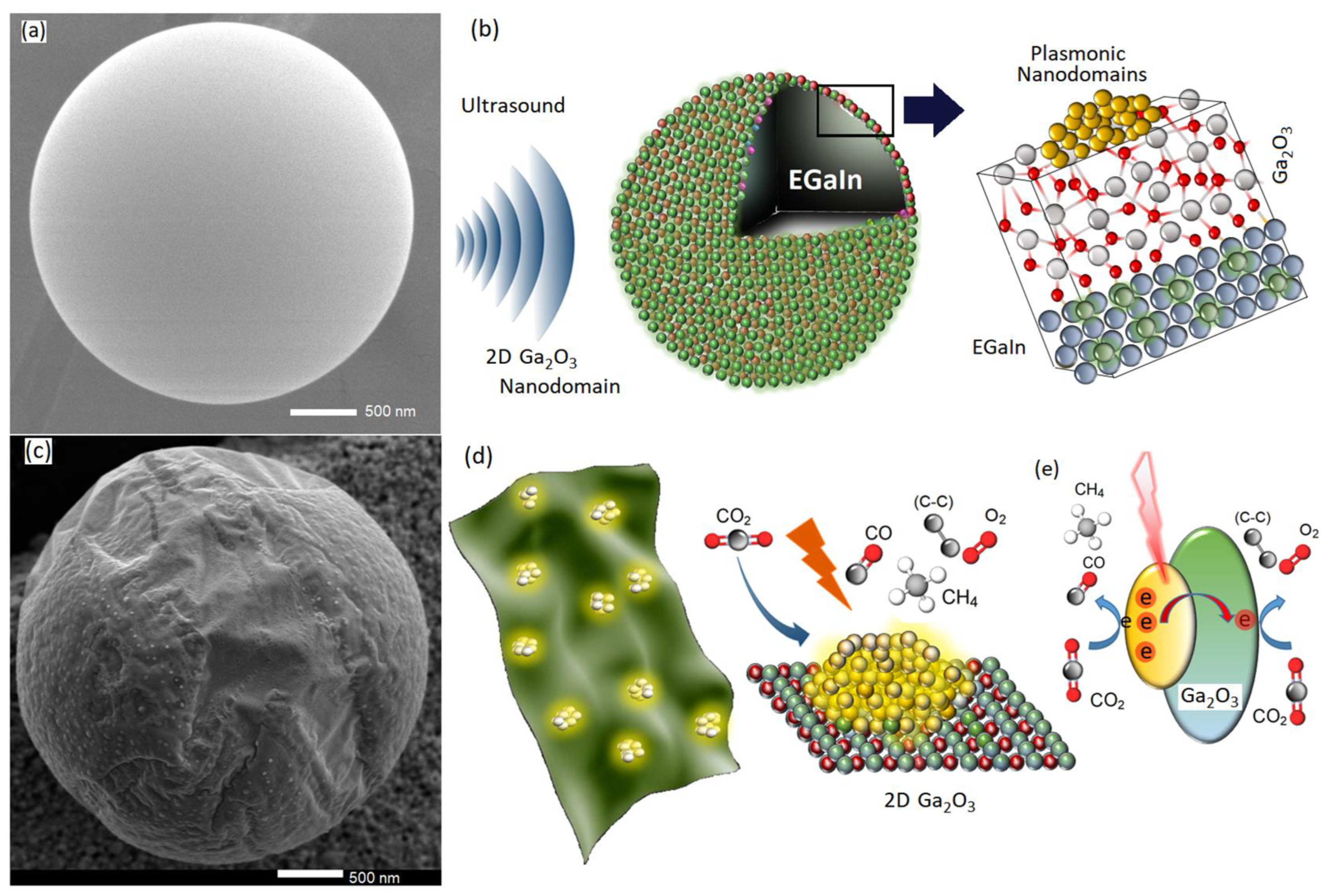
3.1. Synthesis of 2D Ga2O3 Nanosheets with Plasmonic Nanodomains

Generally, 2D materials are synthesized by different techniques. Mechanical exfoliation [33], chemical vapor deposition [34] and atomic layer deposition [35] are among the main commercially available techniques for fabrication of 2D nanostructures. Mechanical delamination of 2D layers of brittle structures in fluid medium is one of the most efficient techniques for large-scale synthesis of 2D materials [36]. The high surface tension of room-temperature liquid metal galinstan effectively suppresses the fragmentation of this alloy into ultrafine nanoparticles (NPs). Ultrasonic waves provide strong mechanical forces for functional applications [37]. Here, we developed a new concept to synthesize 2D Ga2O3 nanostructures from a gallium-based alloy. The ultrasonic waves were able to separate the natural surface oxide film of an EGaInSn alloy from its parent alloy (Figure 1b,c). The outward explosion and also the inward implosion of bubbles during sonication produce microjets and shock waves at ultrasound speeds that also accelerated the moving particles inside the liquid medium at several hundred meters per second (m/s) [38]. The high-energy/high-speed microjets provide strong shear forces for drastic mechanical fragmentation of materials, known as the sonofragmentation process [30,31,32,33,34,35,36,37,38,39,40,41]. Consequently, the acoustic-activated energy can effectively supply the driving force for sequential delamination of 2D surface oxide Ga2O3 nanosheets from their parent EGaInSn alloy [42]. Apart from the mechanical delamination of surface oxide 2D nanosheets, the ultrasonic waves are capable of synthesis of various types of nanostructures. The generated hot-spot regions in the ultrasonic process carry a high temperature (5000 K) and pressures (1000 atm) providing the supplied energies with a magnitude of 13 eV [43]. The high-energy particle collisions, plasma generation [43,44] and nuclear fusion [45] are observed in hot-spot regions generated during ultrasonication. Cooperative interactions between the precursors and ionic species inside acoustic bubble cores result in the synthesis of a wide range of nanostructured materials. The synthesis driving force is provided by the extremely unusual conditions in the core of hot-spot regions [46,47]. In detail, the diffusion of precursors into hot-spot cores is accompanied by the interaction of precursors and other components in the reaction medium, resulting in the synthesis of new nanostructures. The synthesized hot materials in the core of hot spots suddenly quench at the rate of 1010 K/s [48] after the eruption of magma matter into the surrounding fluid environment. The generated thermal shocks enable the immediate growth of various types of nanostructures [49]. Chemical reactions may also occur outside hot-spot regions due to interactions between ionic species and scattered radicals. In this mechanism, the synthesis conditions are free from the extraordinary physical states of hot spots. Therefore, the synthesized materials have properties similar to conventional nanostructures [46]. The control of precursor concentration and the reaction parameters fundamentally affect the sonochemical reactions and prompt the synthesis of new materials with stabilized growth directions. The sonochemical-assisted synthesis of 2D Ga2O3 in metal-ionic solutions enables the growth of crystalline nanostructures on the surface of 2D materials (Figure 1d). Here, the 2D Ga2O3 nanosheets act as the nucleation cites for growth of various nanostructures, including metallic nanodomains. The acoustic-assisted decoration of 2D nanostructures with crystalline nanodomains enables the development of 2D hybrid plasmonic interfaces. The plasmonic nanodomains decorated on 2D Ga2O3 nanosheets alter the electronic properties and energy band alignment at the metal–semiconductor plasmonic heterointerfaces. It is expected that the visible-light properties of these plasmonic 2D structures favor the solar-powered physical and chemical reactions during CO2 conversion through transfer of plasmonic-generated hot carriers into surrounding reaction locations (Figure 1d,e). The mechanism of CO2 conversion will be discussed later.

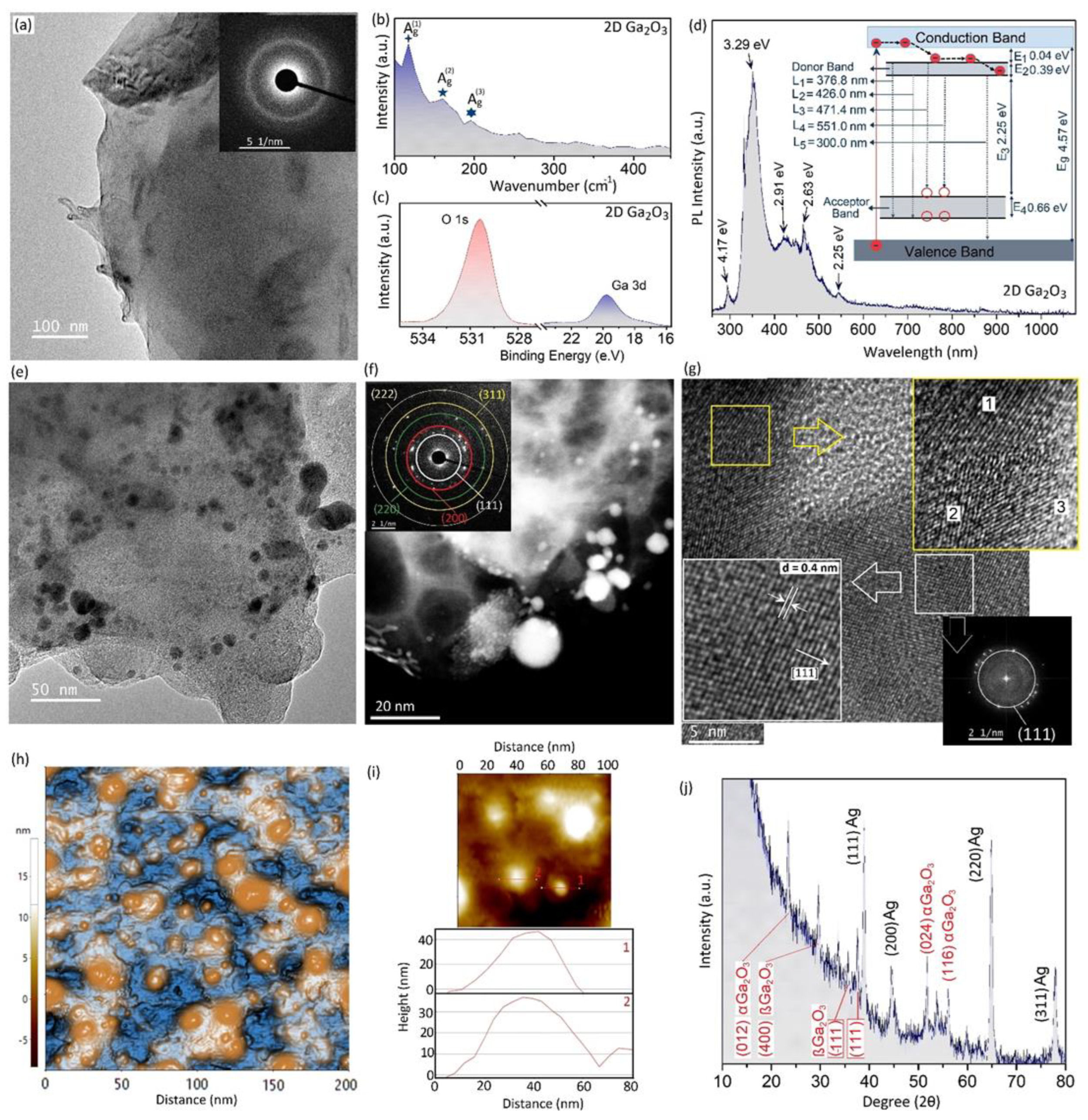
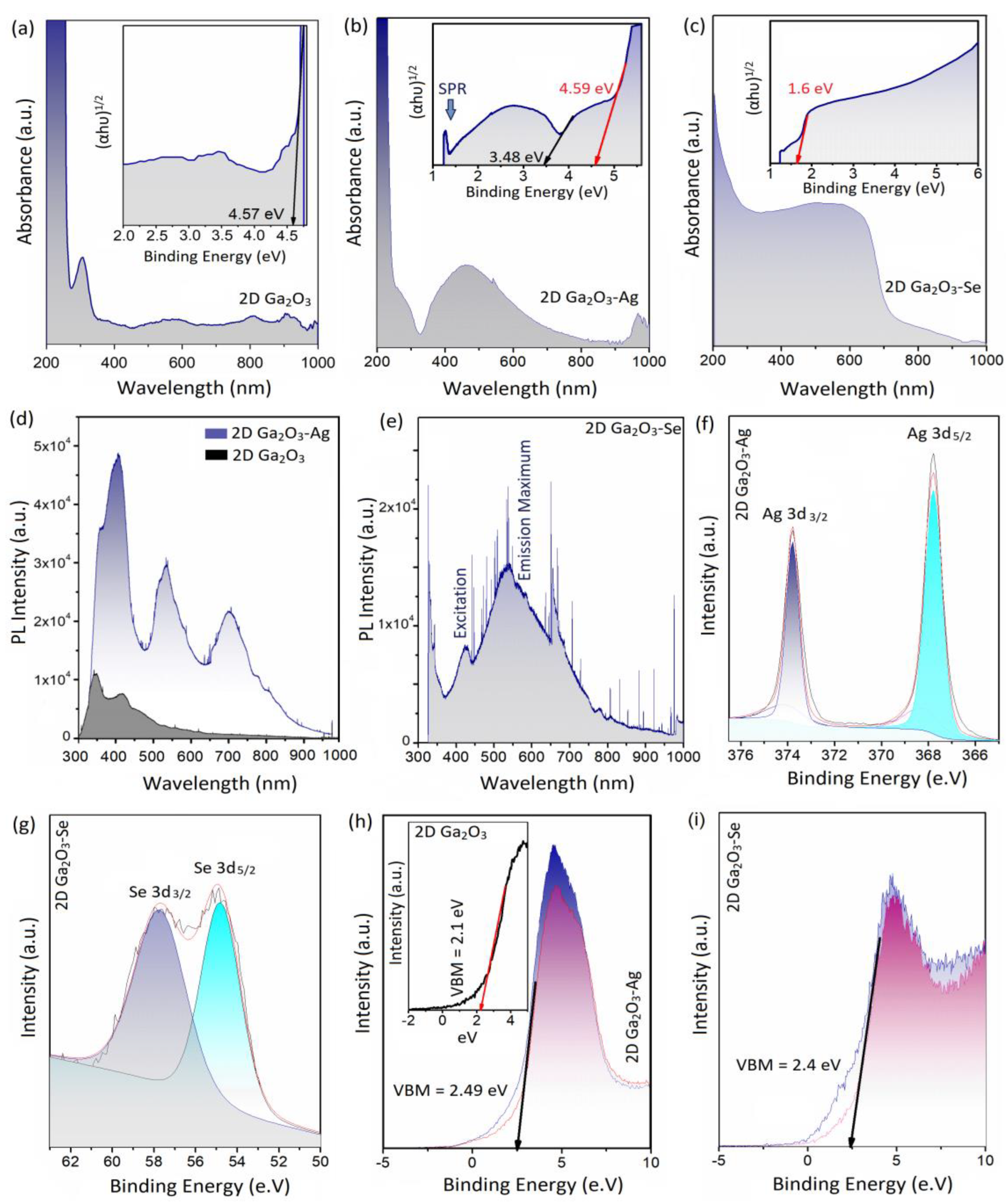
3.2. Characterization of 2D Ga2O3 Nanosheets

We initially investigated the properties of pristine 2D Ga2O3 nanosheets by characterization techniques. The TEM image and its corresponding SAED patterns of pristine 2D Ga2O3 nanosheets depict the halo rings confirming the disordered structural characteristics of these 2D nanostructures (Figure 2a). Therefore, it is expected that pristine 2D Ga2O3 has an amorphous nature. The thickness of pristine Ga2O3 nanosheets was in the range of a few nanometers to tens of nanometers (few cases). The lateral dimensions of 2D nanosheets were in the range of hundreds of micrometers. The following studies by Raman spectroscopy showed the characteristic peaks of A g 1   A g 2 and A g 3 , respectively, at 114 cm−1, 166 cm−1 and 199 cm−1 (Figure 2b). These peaks are related to the vibrational mode of ß-Ga2O3 structure [50]. The following XPS studies evidently showed the Ga 3d peak at 19.9 eV. The distinguished O 1s peak with central position of 529.6 eV is the characteristic peak of oxygen atoms, which is bonded to Ga atoms in Ga2O3 structures (Figure 2c). We further investigated the PL spectra of pristine 2D Ga2O3 nanosheets with a UV laser with λ = 280 nm wavelength. Figure 2d shows the typical PL spectra of pristine 2D Ga2O3 nanosheets. The PL spectra are characterized by several peaks. Two sharp peaks centered at ~300 nm and ~376 nm of the UV region and two peaks centered at ~426 nm and ~471.4 nm in blue regions were observed. A singular peak was also detected at 551.04 nm in the green region of spectrum. The relative intensity of UV luminescence is considerably higher than that of the peaks at blue and green regions (Figure 2d). The PL emission can be attributed to transition of electrons from the donor band to the acceptor and valence bands of 2D Ga2O3 [51]. Due to the disordered nature of pristine 2D nanosheets, it is expected that nonradioactive recombination occurs during the PL emissions [52]. In Figure 2d, the major emission bands are detected at 376.8 nm (L1, 3.29 eV), 426.0 nm (L2, 2.91 eV), 471.4 nm (L3, 2.63 eV), 551.0 nm (L4, 2.25 eV), and an individual minor peak at ~300.0 nm (L5, 4.17 eV). The detection of UV emission in pristine 2D Ga2O3 can be explained by a model that suggests the electrons and holes can be de-trapped due to photoexcitation [52,53]. The migration and incidence of these electron–hole pairs can form self-trapped excitons. These excitons can recombine and emit UV photons [52,53]. A similar mechanism for UV emission was previously reported for single crystal and nanostructured ß-Ga2O3 [52,53]. The UV-green emission in non-doped Ga2O3 structure can be attributed to the recombination of an electron on the donor band of Ga2O3 with another hole formed in the acceptor band of this material [54]. The oxygen vacancies and Ga2+ form a donor band, while the acceptor band can be formed by the gallium vacancy and pairs of gallium–oxygen vacancy [52]. A simplified model is extracted from the PL spectra of 2D pristine Ga2O3 nanosheets and is shown in Figure 2d. The donor band (E1) is located 0.04 eV below the conduction band minimum (CBM), which is attributed to the formed oxygen vacancies [52,54]. The electron photoexcitation from conduction band to valence band is accompanied by electron relaxation where the electron can freely move from conduction band to donor band before the occurrence of radiative recombination. The following electron–hole recombination between donor and acceptor bands yields in the generation of UV-green emission in the PL spectra of pristine Ga2O3 nanosheets (Figure 2d). We further analyzed different energy levels in the bandgap of pristine 2D Ga2O3 nanosheets, and the results are presented in the following lines and depicted in Figure 2d:
E (L1) − E (L2) = E2 = 0.39 eV
E (L3) − E (L4) = E2 = 0.39 eV
E (L1) − E (L3) = E4 = 0.66 eV
E (L2) − E (L4) = E4 = 0.66 eV
Eg (4.57 eV) − E1 − E2 = 4.17 eV
These results are employed to depict the energy band level for pristine Ga2O3 nanosheets (Figure 2d). The calculated value in (5) is equal to 4.17 eV, which is consistent with the energy level of detected minor peaks at ~300.0 nm. This emission is related to the recombination of electrons in the donor band with the holes in valence band edge [52].
The functionalization of 2D Ga2O3 nanosheets with plasmonic nanodomains was successfully achieved by sonochemistry-assisted technique. Figure 2e shows transparent 2D Ga2O3 nanosheets with Ag nanodomains on its surface. The silver NPs can be decorated on the Ga2O3 surface oxide of galinstan alloy either before or after delamination of 2D nanosheets from their parent alloy. It is believed that the 2D Ga2O3 nanosheets act as the nucleation cites for Ag NPs. Furthermore, the gallium on the surface of liquid–metal alloy can also take part in a galvanic reaction where the Ga0 atoms can be replaced by the ionic Ag+ according to the following Equation (6) [55]:
Ga0 + 3Ag+ → Ga3+ + 3Ag0
Ag nanodomains with average size of less than ~20 nm were grown during sonochemical synthesis on 2D Ga2O3 nanosheets. The TEM dark-field image (Figure 2f) shows the distribution of Ag NPs on 2D nanosheets. The distribution of Ag nanostructures on surfaces of 2D nanosheets confirms that these nanodomains grew independently during sonication. The SAED patterns of the same position on 2D nanosheets were collected and are presented in Figure 2f. The diffraction patterns show the growth of various crystalline planes of Ag i.e., (111), (200), (220), (331) and (222) [56]. Figure 2g presents an HRTEM image of two adjacent Ag NPs, their atomic arrangements and corresponding high-resolution fast Fourier-transform (FFT) pattern of an individual region. The HRTEM image in top-right section of Figure 2g demonstrates the heterojunction between three individual nanodomains with different crystalline growth directions. These regions are marked with numbers 1, 2 and 3. It further confirms that Ag nanodomains nucleated and grew individually at different locations on 2D Ga2O3 nanosheets without any preferential growth direction. The more detailed observations in Figure 2g (bottom-left) show the crystalline planes with corresponding distance of 0.4 nm. This interlayer distance can be attributed to the planar space between (111) planes of crystalline Ag nanodomains, which is also confirmed by the results of FFT studies (Figure 2g) [56]. The following study on the 2D Ga2O3 nanosheets by AFM shows the morphology of 2D Ga2O3 nanosheets and Ag nanostructures on it (Figure 2h). The Ag nanostructures on 2D nanosheets can be distinguished vividly. The thickness profiles of two individual Ag NPs are measured and presented in Figure 2i. A typical Ag nanostructure has the dimension of 20 nm (Figure 2i). The AFM studies provide valuable information about the morphology and surface characteristics of 2D Ga2O3 nanosheets and Ag nanodomains. Ag nanodomains grew uniformly on the surface of 2D Ga2O3 nanosheets. The XRD pattern of functionalized 2D Ga2O3-Ag nanosheets is depicted in Figure 2j. The XRD characteristics of crystalline planes of (111), (200), (220) and (311) of Ag are found, which are in agreement with JCPDS 04-0783 [56]. The other characterized peaks can be attributed to the crystalline planes of α- and ß-Ga2O3. It confirms the growth of crystalline phases of gallium oxide during the sonochemical synthesis process.
Material characterization studies also further confirmed the crystalline nature of synthesized Ag nanodomains decorated on the surface of 2D Ga2O3 nanosheets.
We further characterized the 2D Ga2O3-Se nanosheets. Figure 3a depicts a TEM image of 2D Ga2O3-Se nanosheets. The ultrasonic waves create extreme localized hot spots that enable complex physicochemical reactions. At the Ga2O3 surface, the interfacial reactive wetting is enhanced due to intensified turbulence, which consequently prompts a high level of ion mobility and mass transfer from the Se ionic regions to the surface of 2D Ga2O3. Generally, Se forms in amorphous, metallic and crystalline polymorphs [57]. Low melting (217 °C) and low glass transition (31 °C) temperatures facilitate the synthesis of amorphous Se at room temperature that can be transformed into trigonal Se in the conventional thermal synthesis methods [58]. The ultrasonic waves enabled the synthesis of Se nanostructures in unusual non-thermodynamic conditions [59]. At the initial stage of sonication treatment of the samples in Se containing ionic solution, the sequential decomposition of SeCl4 into Se2Cl2 and HCl leads to the rapid nucleation of Se nanostructures on nucleation sites of 2D Ga2O3. The Se atoms tend to form mono-Se particles on 2D Ga2O3 structures due to the elevated reactive wetting. Upon the increase in sonication time, Se nanostructures actively nucleate and grow on the surface of 2D nanosheets, which later agglomerate in the form of Se clusters and nanodomains. Figure 3b depicts the Se nanocrystalline structure with its corresponding HRTEM image. The HRTEM image shows the crystalline interlayer distance of 0.39 nm in the crystalline direction of (110). The following study on the SAED patterns of synthesized Se nanodomains confirmed the presence of crystallographic planes of (101), (110), (102) and (201) attributed to the crystalline Se nanostructure (Figure 3c) [60,61]. The flowing AFM studies on the surface morphology and characteristics of 2D Ga2O3-Se nanosheets depict the distribution of both singular and agglomerated Se nanostructures on the surface of 2D Ga2O3 nanosheets (Figure 3d). In some rare cases, the Se nanodomains formed clusters with an average size of 50 nm (Figure 3d). However, in most typical examples, the size of the Se nanodomains was less than 20 nm. Figure 3e provides the thickness profile of a Se nanodomain and its 3D surface morphology. We further investigated the crystalline state of synthesized Se nanodomains via XRD. To this end, 2D Ga2O3 nanosheets were sonicated in a solution containing 1 μmol SeCl4 in ethyl alcohol anhydrous. The extracted nanosheets were later dried in controlled atmosphere and tested. It was observed that the surfaces of samples were covered with a red-tinted Se layer. The XRD results confirmed the presence of planes of (100), (101) (110) 102) and (201) related to the crystalline plane of Se (JCPDS 06-0362) [62]. These results further confirmed the polycrystalline nature of sonochemically synthesized Se nanostructures.
UV-vis and PL spectroscopy are functional methods for investigation of photonic properties of 2D plasmonic structures. The bandgap measurements of 2D Ga2O3 and Ga2O3-Ag nanosheets gave interesting information on the electronic characteristics of them. The typical absorbance spectra (UV-vis test) of 2D Ga2O3 and Ga2O3-Ag nanosheets are presented in Figure 4a,b, respectively. The calculated (inset in Figure 4a) bandgap of ~4.57 eV can be attributed to the bandgap of pristine 2D Ga2O3 nanosheets. The typical absorbance spectrum of 2D Ga2O3-Ag nanostructures is also demonstrated in Figure 4b. The following calculations showed two individual bandgaps of ~4.59 eV and ~3.48 eV. The higher bandgap (4.59 eV) can be attributed to semiconducting characteristics of 2D Ga2O3 nanosheets. The Gaussian peak at 400 nm~500 nm was observed in absorption spectra of 2D Ga2O3-Ag nanosheets (Figure 4b). Similar observations were also reported in a study of UV-vis characteristics of synthesized silver nanoparticles [63]. This peak is attributed to the optical direct bandgap of silver nanoparticles, which was 3.48 eV in the present study. This number is mostly in agreement with the previously reported bandgap of silver NPs [63]. Furthermore, the plasmonic characteristics of Ag NPs can be responsible for the absorption peak at vicinity of 400 nm [64]. The strong plasmonic resonance absorption peak at the vicinity of λ = 410~430 is one the main characteristics of Ag nanoparticles known as the plasmonic resonance absorption peak [65,66]. The location and intensity of the plasmonic resonance peak are affected by the dimensions of silver NPs. It was shown that the plasmonic resonance absorption of Ag NPs with particle sizes of 10–20 nm occurs at the vicinity of λ = 400 nm [66]. It was reported that an increase in Ag particle size results in the increased scattering, and therefore the plasmonic resonance absorption peak broadened and shifted toward higher wavelengths, known as red shift of light [67]. The plasmonic resonance absorption peaks in this study were due to the presence of ultrafine Ag plasmonic nanoparticles decorated on 2D Ga2O3 nanosheets. The evidence of occurrence of surface plasmon resonance (SPR) was also observed by the detection of the broad peak at λ~500 nm related to the plasmonic characteristics of Ag nanodomains [66]. The photonic local field enhancement and SPR occurred at heterointerfaces between Ag nanodomains at 2D Ga2O3. Consequently, the SPR characteristic peaks appeared at absorption spectra of Ga2O3-Ag heterointerfaces. In practice, the refractive index of the adjacent environment considerably affects the extinction spectrum [67]. A high refractive index for materials similar to 2D Ga2O3 nanosheets can cause a red shift in the location of the extinction peak. The Ag nanodomains of this research are in contact with 2D Ga2O3 and air; therefore, the transfer of resonance adsorption and SPR peaks to higher wavelengths is expected in absorbance spectra of 2D Ga2O3-Ag nanostructures. The study on UV-vis spectra of 2D Ga2O3-Se nanosheets showed a bandgap of 1.6 eV, which is the characteristic bandgap of Se crystalline nanostructures (Figure 4c) [68].
In the PL spectroscopy, it is possible to focus on an individual 2D Ga2O3 nanosheets and collect the PL spectra of 2D nanostructures. Figure 4d depicts the PL spectra of pristine 2D Ga2O3 and 2D Ga2O3-Ag nanostructures. The PL spectra of 2D Ga2O3-Ag nanosheets demonstrate three individual peaks at wavelengths of 380 nm, 550 nm, and ~700 nm. These peaks originate from the PL characteristics of Ag nanoparticles enhanced by the strong local electric field of Ag nanodomains [69]. The peak around 340–400 nm is attributed to the interband radiative transitions in Ag nanoparticles [69]. The shoulder in the PL spectrum at 345 nm is close to the maximum of the PL band of bulk silver that occurs at 330 nm. This peak is attributed to the direct radiative interband recombination between the electrons in the conduction band and holes in the valence band of silver that had been scattered to momentum states (less than the Fermi momentum). The intense peak at 390 nm (3.2 eV) is quite close to the intraband absorption edge of bulk silver [69]. The recognized red shift in PL peaks of these NPs (compared with bulk silver) is due to the coupling of the exciting and emitted photons with SPR [69]. The peak in the vicinity of 450–500 nm is also close to the SPR of silver NPs. Therefore, this peak originated from the low-energy wings of the intraband PL peak and is enhanced by the SPR effects. Similar results were also observed in a study of PL spectra of Ag NPs, where the PL bands were located in the vicinity of SPR peaks [69]. The typical PL spectra of 2D Ga2O3-Se nanostructures are presented in Figure 4e. The PL studies on the same sample demonstrate two peaks at the λ = 340 nm, and λ = 427, and another broad peak centered at λ = 558 nm. These peaks (λ = 427 nm and λ = 558 nm) are respectively related to the excitation and emission peaks of Se nanodomains [68]. Another peak at λ = 650 nm was also detected. The broad peak at λ = 558 nm and the peak at λ = 650 are attributed to the excitation of surface plasmon of Se nanostructure. The red tint of synthesized 2D Ga2O3-Se nanostructures has been ascribed to the corresponding excitation of the surface plasmon resonance of Se nanostructure [70]. It appeared that the heterointerfaces between of 2D Ga2O3 nanosheets and Se nanodomains possessed a high level of blue luminesce peak. The PL spectra of 2D Ga2O3-Se is quite interesting, since the peaks of green and red luminescence are stronger than those of UV luminescence peaks. The Se nanostructures are well known for their photonic, photovoltaic, and semiconducting properties; therefore, these nanostructures can extensively contribute to the performance of 2D Ga2O3 nanosheets for photonic applications. It is worth mentioning that UV luminescence is affected by the recombination at the surface states by the surface characteristics of materials [71]. The dangling bands and other surface impurities act as the recombination cites for carriers. The presence of metallic nanodomains on the surface can enhance the density of permanent surface defects and therefore influence the PL intensity of 2D Ga2O3 nanosheets [71]. In blue and red luminescence phenomena, both electrons and holes are trapped in donor and acceptor levels within the bulk structure of materials. In contrast, it is expected that the photoexcited conduction band electrons diffuse to the surface of 2D nanosheets and then are trapped in the structural defects at surface of the Ga2O3 nanosheets decorated with crystalline nanoparticles. This phenomenon increases the possibility of non-radiative recombination and therefore affects the intensity of UV photoluminescence intensity [71].

3.3. Solar-Powered Acoustic-Activated CO2 Conversion

The gas adsorption on catalyst surface is one of the main characteristics of synthesized 2D materials. We investigated the in situ adsorption of CO2 gas on the surface of 2D Ga2O3 nanosheets via FT-IR. FT-IR spectra were recorded in absorbance mode on a Nicolet spectrometer equipped with a quartz gas chamber with KBr windows. To this end, a quartz chamber containing 2D Ga2O3 nanostructures was used in the FTIR machine and the adsorption characteristics were monitored sequentially at different stages of reactions. Figure 5a depicts the dynamic absorbance spectra of 2D Ga2O3-Ag nanostructures in sealed quartz chamber containing highly pure dry CO2 gas at room temperature. These results clearly showed that the adsorption of CO2 on the surface of 2D Ga2O3 nanosheets was accompanied by the formation of number of distinct carbonate and hydroxyl species on the surface. The detection and assignment of these carbonate groups are based on the last studies on CO2 adsorption process on Ga2O3 polymorphs [72]. A closer look at Figure 5a revels that the increase of reaction time leads to the formation of distinct signals of CO2 at ~2350 cm−1. Furthermore, the intensities of corresponding absorbance peaks of other carbonate groups also increased (Figure 5a). In detail, the intensities of the adsorption peaks at 1165 cm−1 (bicarbonate HC O 3 ), 1335 cm−1 (bicarbonate vs(OCO)), 1377 cm−1 (bicarbonate vs(CO3)), 1528 cm−1 (vas(C O 3 )), 1656 cm−1 (bridged carbonate vas(C O 3 )), and 1793 cm−1 (monodentate bicarbonate (vas(CO3)) increased vividly during interaction of 2D Ga2O3-Ag nanostructures with CO2 gas [73]. These results confirm the adsorption of CO2 and also the formation of various carbonate groups on the surface of 2D Ga2O3-Ag nanostructures. The detection of bicarbonate and monocarbonate groups is correlated with the adsorption of hydroxyl groups on the surface of 2D Ga2O3 nanosheets. It is realized that the fundamental stage in CO2 conversion is the chemisorption of CO2 molecules on the 2D Ga2O3 nanosheets via insertion into a basic hydroxyl group on the surface of 2D metal oxide nanosheets. This process leads to the formation of bicarbonate groups [73,74]. We further investigated the FTIR absorbance spectra of 2D Ga2O3-Se nanostructures under the dynamic exposure to the CO2 gas. A typical dynamic absorbance FTIR spectra of 2D Ga2O3-Se nanosheets demonstrates continues increase in the intensity of bicarbonate peaks (Figure 5b). A comparison between Figure 5a and b shows that the peak intensities of bicarbonate and monodentate bicarbonate groups on the surface of 2D Ga2O3-Se nanostructures are tangibly stronger than those of 2D Ga2O3-Ag structures. A possible explanation can be attributed to the effect of Se on the absorption of hydroxide groups on the surface. Se actively reacts with the hydroxyl groups in atmosphere. It can explain the higher intensity of absorption peaks of carbonates groups on the 2D Ga2O3-Se nanostructures, compared with that of 2D Ga2O3-Ag nanosheets. Therefore, the in situ FTIR results confirmed the time-dependent increasing capability of synthesized 2D nanostructures for chemisorption of CO2 molecules. We further investigated the CO2 conversion efficiency of these 2D nanostructures. Regarding the distinguished photonic and plasmonic properties of 2D Ga2O3-Ag and 2D Ga2O3-Se nanostructures, the solar-powered CO2 conversion capacity of these 2D nanostructures is investigated in the next section. Furthermore, we used the ultrasonic generators to combine the effects of acoustic waves and solar radiation for synergistic conversion of CO2 gas molecules.
Acoustic-activated CO2 reduction has recently been developed for efficient conversion of CO2 into value-added byproducts in the presence of gallium and Ga2O3 based catalyst nanostructures [75]. Driven by effects of acoustic energies, the efficient CO2 conversion was achieved when gallium-based nanoparticles were used as catalyst materials [75]. It is confirmed that the strong mechanical triboelectric forces efficiently provide the energy for CO2 conversion [75]. The sonochemical triboelectric forces contribute the interfacial phenomena in the heterointerfaces of catalyst materials. In the present study, we innovatively used both mechanical energy of acoustic waves and the solar-powered plasmonic effects to enable the efficient conversion of CO2. To this end, we designed a transparent quartz reactor was submerged in an ultrasonic bath (Figure 5c). The solar-powered energy was supplied by a solar simulator xenon lamp at the power of 250 W and output wavelength of 350–1100 nm (Figure 5c). It is worth mentioning that we investigated the amounts of CO2 and O2 in the input and exhaust gases to show the efficiency of our conversion technique. Therefore, precise CO2/O2 sensors with 10 ppm measurement limit were employed to monitor the input and exhaust gases. It should be mentioned that chamber was totally sealed and the process of extraction of exhaust products was done by the collection of output gases via a sealed gas box, mounted on the nozzle of the sonication system. After the CO2 conversion process, the solid byproducts of reactions were found suspended on the quartz vials (Figure 5d). After filtration of byproducts, the samples were investigated by SEM and TEM. The SEM image, EDX line analysis and corresponding SAED patterns of TEM studies are presented in Figure 5c. The EDS analysis confirmed that the extracted byproducts are composed of 83 wt.% carbon. The TEM studies showed halo rings in SAED patterns confirming the amorphous nature of carbon byproducts (Figure 5d). The exhaust gases were measured by the ppm level CO2 and O2 sensors to calculate the CO2 conversion efficiency of system. Figure 5e depicts the remaining CO2 content after the conversion process. It is necessary to mention that the exhaust gas is able to circulate in the reaction chamber. Therefore, the CO2 content was measured after 5, 10, 15, 20, 25 and 30 min from the start of cyclic conversion. It can be observed that the CO2 percentage decreased considerably in both 2D Ga2O3, 2D Ga2O3-Ag, and 2D Ga2O3-Se samples under solar radiation and mechanical agitation of acoustic waves. Results show that the triboelectric and photocatalytic mechanisms can lower the CO2 content to less than 20% after 30 min of cyclic reactions in the chamber containing pristine 2D Ga2O3 nanosheets. However, the effect of solar radiation on photonic conversion of CO2 became more visible when the 2D Ga2O3-Ag and 2D Ga2O3-Se nanosheets were employed in the reaction chamber. In an optimized case, the CO2 content in exhaust gases declined to the values less than 5% after 30 min of sequential conversion in the chamber containing 50 gr/L concentration of 2D Ga2O3-Ag nanosheets under 250 W radiation of solar-light simulator. Therefore, 94.6% CO2 conversion efficiency was achieved. This high conversion efficiency is gained through the combined effects of plasmonic photocatalysis accompanied by the acoustic-activated CO2 conversion mechanisms. The photonic mechanism of CO2 conversion can be explained based on the generation of hot electrons at plasmonic heterointerfaces (Figure 1e). In these 2D heterointerfaces, the plasmonic-generated hot electrons are transferred to the adjacent 2D Ga2O3 semiconductor to enable the conversion of adsorbed CO2 into O2 and carbon. The triboelectric forces accompanied by plasmonic nanostructures can activate the mechanism of C = O debonding and then enable the conversion of CO2 atoms into value-added byproducts [31,75]. Therefore, the photogenerated hot electrons at plasmonic 2D heterointerfaces between Ag and Se nanodomains and 2D Ga2O3 nanosheets have provided the excess electrons for the CO2 conversion through these reactions:
Electron   ( e 1 ) + CO 2   hole   ( h + ) + C O 2 °
C O 2 ° + e     CO   +   h +   +   O 2
CO + 2   e     C   +   2 h +   +   O 2
2 O 2     O 2   +   4 e
In these reactions, the plasmonic–triboelectric generated electron transfer to CO2 (Equation (7)). The following electron transfer to C O 2 ° radicals was accompanied by the generation of CO and O2− radicals (Equations (8) and (9)). The CO later turns into carbon-based materials, while the O2− turns into O2 after reduction (Equation (10)) [75]. We further investigated the CO2 conversion efficiency of 2D Ga2O3-Se nanostructures. Interestingly, in the similar conditions, the CO2 conversion efficiency of 2D Ga2O3-Se nanostructures was less than that of 2D Ga2O3-Ag nanostructures after 30 min of cyclic reactions in reactor. Despite the lower efficiency, the 2D Ga2O3-Se nanostructures still present a high CO2 conversion efficiency (higher than 92%) (Figure 5e). In the case of 2D Ga2O3-Se nanostructures, the effect of piezoelectric Se nanodomains should also be considered. The piezoelectric CO2 conversion was recently investigated in several studies. In this mechanism, it is expected that the 2D Ga2O3-Se heterointerfaces provide extra electrons to break the strong sp hybridization of CO2 atoms and activate the piezocatalytic conversion of CO2 into value-added by products [76]. The high-frequency ultrasound waves continuously polarize the 2D Ga2O3-Se heterointerfaces and establish the built-in electric field at the 2D piezoelectric structure. Consequently, electron–hole pairs are separated continuously from each other and move to opposite surface of piezoelectric material [76]. We further collected the carbon-rich byproducts of reactions to calculate their production rate. After stabilization of CO2 conversion in the chamber containing 2D Ga2O3-Ag nanosheets, the amount of ~180 μmol/g−1 of solid carbon was extracted after 30 min of catalysis reaction, which is equal to the carbon production rate of ~360 μmol g−1h−1 (Figure 5f). This number is higher than the conversion rate of most of the previously reported conversion performance of 2D-based photocatalysts for CO2 reduction (Table 1).
Table 1. A list of 2D materials employed for CO2 conversion process.
MaterialsSource of EnergyConversion Product & RateRef.
Ga2O3-Ag250 W Xenon-lamp + ultrasonic (20 Hz, 380 W)Solid carbon; ~360 μmol g−1h−1Present
TiO2 nanosheets300 W Hg lampHCOOH; 1.9 μmol g−1h−1[77]
TiO2 nanosheets/graphene300 W Xe lampCO; 52.3 μmol g−1h−1[78]
SnS2/TiO2 nanosheets300 W Xe lampCH4; 23.0 μmol g−1h−1[79]
Cu2O octahedrons/WO3 nanoflakes composite300 W Xe lampCO; 3.45 μmol g−1h−1[80]
ZnV2O6 nanosheet/RGO nanosheet35 W HID Xe lampCH3OH; 515.4 μmol g−1h−1[81]
Graphene bridged ZnV2O6/pCN nanosheets35 W Xe lampCH3OH; 542.92 μmol g−1h−1[82]
BiOBr nanosheets300 W Xe lampCO; 4.45 μmol g−1h−1[83]
Bi4O5Br2 nanosheet300 W Xe lampCO; 31.57 μmol g−1h−1[84]
BiOBr nanosheets with surface Bi vacancies300 W Xe lampCO; 20.1 μmol g−1h−1[85]
MoS2-nanosheets/TiO2-nanosheets300 W Xe lampCH3OH 10.6 μmol g−1h−1[86]
Cs2SnI6/SnS2 nanosheet100 W Xe lampCH4; 6.09 μmol g−1h−1[87]
Ni metaleorganic framework monolayers5 W white LED lightCO; 12,500 μmol g−1h−1[88]
CeO2/Ti3C2350 W Xe lampCO; 40.2 μmol g−1h−1[89]
CsPbBr3/Ti3C2Tx300 W Xe lampCO; 26.32 μmol g−1h−1
CH4 7.25 μmol g−1h−1
[90]

4. Conclusions

In summary, Ag and Se plasmonic polycrystalline nanodomains were grown on the surface of 2D Ga2O3 catalyst via sonochemical assisted synthesis. These 2D heterointerfaces were found highly efficient platforms for plasmonic CO2 photocatalysis in the presence of mechanical energies of acoustic waves. It was observed that the triboelectric energy accompanied by the plasmonic photocatalysis co-contributed to enhance the CO2 conversion efficiency to values higher than 94%. The challenging process of growth of plasmonic Ag and Se nanodomains was crucially dependent on the precursor selection as well as synthesis. The material characterization studies showed the polycrystalline nature of Ag and Se nanodomains grown on the surface of 2D Ga2O3 nanosheets. The AFM studies further confirmed the uniform distribution of plasmonic nanodomains on the surface of 2D nanostructures. PL spectroscopy further confirmed the local field enhancement and surface plasmon resonance (SPR) interactions of Ag and Se nanodomains on 2D Ga2O3 nanosheets. The enhanced CO2 conversion capability of these nanostructures originated from the following factors: the plasmonic photocatalysis at Ga2O3-Ag and Ga2O3-Se heterointerfaces, the plasmonic hot-electron transfer at catalyst interfaces, and finally the acoustic-activated CO2 debonding and conversion. Consequently, this principally developed novel technique for solar-activated acoustic photocatalysis of CO2 into value-added byproducts provides excellent opportunities for establishment of technological platforms for generation of clean fuels similar to O2 through solar-assisted conversion of greenhouse gases.

Author Contributions

Introduction of concept, experiments, original draft preparation, M.K.A. and N.S.L.; supervision of research and evaluation of results, J.P. and S.Z. All authors have read and agreed to the published version of the manuscript.

Funding

This research was funded by Ghent University Global Campus (Republic of Korea).

Institutional Review Board Statement

Not applicable.

Informed Consent Statement

Not Applicable.

Data Availability Statement

Available upon request from authors.

Acknowledgments

This work was supported by a research program of the Ghent University Global Campus, Republic of Korea.

Conflicts of Interest

The authors declare no conflict of interest.

References

  1. Linic, S.; Chavez, S.; Elias, R. Flow and extraction of energy and charge carriers in hybrid plasmonic nanostructures. Nat. Mater. 2021, 20, 916–924. [Google Scholar] [CrossRef]
  2. Wang, M.; Wang, T.; Ojambati, O.S.; Duffin, T.J.; Kang, K.; Lee, T.; Scheer, E.; Xiang, D.; Nijhuis, C.A. Plasmonic phenomena in molecular junctions: Principles and applications. Nat. Rev. Chem. 2022, 6, 681–704. [Google Scholar] [CrossRef] [PubMed]
  3. Gao, B.; Arya, G.; Tao, A. Self-orienting nanocubes for the assembly of plasmonic nanojunctions. Nat. Nanotechnol. 2012, 7, 433–437. [Google Scholar] [CrossRef] [PubMed]
  4. Yu, H.; Peng, Y.; Yang, Y.; Li, Z.Y. Plasmon-enhanced light–matter interactions and applications. NPJ Comput. Mater. 2019, 5, 45. [Google Scholar] [CrossRef] [Green Version]
  5. Koya, A.N.; Zhu, X.; Ohannesian, N.; Yanik, A.A.; Alabastri, A.; Zaccaria, R.P.; Krahne, R.; Shih, W.C.; Garoli, D. Nanoporous metals: From plasmonic properties to applications in enhanced spectroscopy and photocatalysis. ACS Nano 2021, 15, 6038–6060. [Google Scholar] [CrossRef]
  6. Agrawal, A.; Cho, S.H.; Zandi, O.; Ghosh, S.; Johns, R.W.; Milliron, D.J. Localized surface plasmon resonance in semiconductor nanocrystals. Chem. Rev. 2018, 118, 3121–3207. [Google Scholar] [CrossRef]
  7. Wallace, J.; Soham, S.; Vladimir, S.M.; Alexandra, B.; Marcello, F. Transparent conducting oxides: From all-dielectric plasmonics to a new paradigm in integrated photonics. Adv. Opt. Photonics 2022, 14, 148. [Google Scholar]
  8. Karbalaei Akbari, M.; Hai, Z.; Wei, Z.; Detavernier, C.; Solano, E.; Verpoort, F.; Zhuiykov, S. ALD-Developed plasmonic two-dimensional Au–WO3–TiO2 heterojunction architectonics for design of photovoltaic devices. ACS Appl. Mater. Interfaces 2018, 10, 10304–10314. [Google Scholar] [CrossRef]
  9. Xu, H.; Karbalaei Akbari, M.; Verpoort, F.; Zhuiykov, S. Nano-engineering and functionalization of hybrid Au–MexOy–TiO2 (Me = W, Ga) hetero-interfaces for optoelectronic receptors and nociceptors. Nanoscale 2020, 12, 20177–20188. [Google Scholar] [CrossRef]
  10. Stanford, M.G.; Rack, P.D.; Jariwala, D. Emerging nanofabrication and quantum confinement techniques for 2D materials beyond graphene. NPJ 2D Mater. Appl. 2018, 2, 20. [Google Scholar] [CrossRef] [Green Version]
  11. Karbalaei Akbari, M.; Zhuiykov, S. Photonic and plasmonic devices based on two-dimensional semiconductors. In Ultrathin Two-Dimensional Semiconductors for Novel Electronic Applications; CRC Press Tylor and Francis: Boca Raton, FL, USA, 2020; Volume 1, pp. 145–169. [Google Scholar]
  12. Turunen, M.; Brotons-Gisbert, M.; Dai, Y.; Wang, Y.; Scerri, E.; Bonato, C.; Jöns, K.L.; Sun, Z.; Gerardot, B.D. Quantum photonics with layered 2D materials. Nat. Rev. Phys. 2022, 4, 219–236. [Google Scholar] [CrossRef]
  13. Zhuiykov, S.; Karbalaei Akbari, M. Metal/semiconductor hetero-interface engineering for photocurrent controlling in plasmonic photodetectors. In Proceedings of the SMSI 2021-Sensors and Instrumentation, Nuremberg, Germany, 3 May 2021; pp. 165–166. [Google Scholar]
  14. Xu, H.; Karbalaei Akbari, M.; Zhuiykov, S. 2D semiconductor nanomaterials and heterostructures: Controlled synthesis and functional applications. Nanoscale Res. Lett. 2021, 16, 94. [Google Scholar] [CrossRef] [PubMed]
  15. Agarwal, A.; Vitiello, M.S.; Viti, L.; Cupolillo, A.; Politano, A. Plasmonics with two-dimensional semiconductors: From basic research to technological applications. Nanoscale 2018, 10, 8938–8946. [Google Scholar] [CrossRef] [PubMed] [Green Version]
  16. Rossi, T.P.; Erhart, P.; Kuisma, M. Hot-carrier generation in plasmonic nanoparticles: The importance of atomic structure. ACS Nano 2020, 14, 9963–9971. [Google Scholar] [CrossRef] [PubMed]
  17. Karbalaei Akbari, M.; Verpoort, F.; Zhuiykov, S. Bioinspired patterned photonic junctions for plasmon-enhanced metal photoluminescence and fluorescence: Design of optical cavities for near-infrared electronics. Mater. Today Energy 2022, 26, 101003. [Google Scholar] [CrossRef]
  18. Xu, G.; Liu, J.; Wang, Q.; Hui, R.; Chen, Z.; Maroni, V.A.; Wu, J. Plasmonic graphene transparent conductors. Adv. Mater. 2012, 24, OP71–OP76. [Google Scholar] [CrossRef] [PubMed]
  19. Xu, H.; Karbalaei Akbari, M.; Wang, S.; Chen, S.; Kats, E.; Verpoort, F.; Hue, J.; Zhuiyko, S. Tunability of near infrared opto-synaptic properties of thin MoO3 films fabricated by atomic layer deposition. Appl. Surf. Sci. 2022, 539, 153399. [Google Scholar] [CrossRef]
  20. Karbalaei Akbari, M.; Ramachandran, R.K.; Detavernier, C.; Hu, J.; Kim, J.; Verpoort, F.; Zhuiykov, S. Heterostructured plasmonic memristors with tunable optosynaptic functionalities. J. Mater. Chem. C 2021, 9, 2539–2549. [Google Scholar] [CrossRef]
  21. Karbalaei Akbari, M.; Hu, J.; Verpoort, F.; Lu, H.; Zhuiykov, S. Nanoscale all-oxide-heterostructured bio-inspired optoresponsive nociceptor. Nano-Micro Lett. 2020, 12, 83. [Google Scholar] [CrossRef] [Green Version]
  22. Karbalaei Akbari, M.; Zhuiykov, S. Optoelectronic nociceptive sensors based on heterostructured semiconductor films. In Proceedings of the SMSI 2021-Sensors and Instrumentation, Nuremberg, Germany, 3 May 2021; pp. 159–160. [Google Scholar]
  23. Oh, S.H.; Altug, H.; Jin, X.; Low, T.; Koester, S.J.; Ivanov, A.P.; Edel, J.B.; Avouris, P.; Strano, M.S. Nanophotonic biosensors harnessing van der Waals materials. Nat. Commun. 2021, 12, 3824. [Google Scholar] [CrossRef]
  24. Karbalaei Akbari, M.; Siraj Lopa, N.; Shahriari, M.; Najafzadehkhoee, A.; Galusek, D.; Zhuiykov, S. Functional Two-Dimensional Materials for Bioelectronic Neural Interfacing. J. Funct. Biomater. 2023, 14, 35. [Google Scholar] [CrossRef] [PubMed]
  25. Karbalaei Akbari, M.; Zhuiykov, S. A bioinspired optoelectronically engineered artificial neurorobotics device with sensorimotor functionalities. Nat. Commun. 2019, 10, 3873. [Google Scholar] [CrossRef] [PubMed] [Green Version]
  26. Wang, L.; Huang, L.; Tan, W.-C.; Feng, X.; Chen, L.; Huang, X.; Ang, K.-W. 2D photovoltaic devices: Progress and prospects. Small Methods 2018, 2, 1700294. [Google Scholar] [CrossRef]
  27. Berquist, Z.J.; Turaczy, K.K.; Lenert, A. Plasmon-enhanced greenhouse selectivity for high-temperature solar thermal energy conversion. ACS Nano 2020, 14, 12605–12613. [Google Scholar] [CrossRef] [PubMed]
  28. Gao, D.; Arán-Ais, R.M.; Jeon, H.S.; Cuenya, B.R. Rational catalyst and electrolyte design for CO2 electroreduction towards multicarbon products. Nat. Catal. 2019, 2, 198–210. [Google Scholar] [CrossRef]
  29. Ackermann, S.; Sauvin, L.R.; Castiglioni, R.; Rupp, J.L.M.; Scheffe, J.R.; Steinfeld, A. Kinetics of CO2 reduction over nonstoichiometric ceria. J. Phys. Chem. C 2015, 119, 16452–16461. [Google Scholar] [CrossRef] [Green Version]
  30. Karbalaei Akbari, M.; Verpoor, F.; Zhuiykov, S. State-of-the-art surface oxide semiconductors of liquid metals: An emerging platform for development of multifunctional two-dimensional materials. J. Mater. Chem. A 2021, 9, 34–73. [Google Scholar] [CrossRef]
  31. Verma, R.; Belgamwar, R.; Polshettiwar, V. Plasmonic photocatalysis for CO2 conversion to chemicals and fuels. ACS Mater. Lett. 2021, 3, 574–598. [Google Scholar] [CrossRef]
  32. Karbalaei Akbari, M.; Hai, Z.; Zhuiykov, S. Wafer-scale two-dimensional Au-TiO2 bilayer films for photocatalytic degradation of Palmitic acid under UV and visible light illumination. Mater. Res. Bull. 2017, 95, 380–391. [Google Scholar] [CrossRef]
  33. Huang, Y.; Pan, Y.H.; Yang, R.; Bao, L.H.; Meng, L.; Luo, H.L.; Cai, Y.Q.; Liu, G.D.; Zhao, W.J.; Zhou, Z.; et al. Universal mechanical exfoliation of large-area 2D crystals. Nat. Commun. 2020, 11, 2453. [Google Scholar] [CrossRef]
  34. Karbalaei Akbari, M.; Zhuiykov, S. Chemical vapor deposition of two-dimensional semiconductors. In Ultrathin Two-Dimensional Semiconductors for Novel Electronic Applications; CRC Press Tylor and Francis: Boca Raton, FL, USA, 2020; Volume 1, pp. 1–33. [Google Scholar]
  35. Karbalaei Akbari, M.; Zhuiykov, S. Atomic layer deposition of two-dimensional semiconductors. In Ultrathin Two-Dimensional Semiconductors for Novel Electronic Applications; CRC Press Tylor and Francis: Boca Raton, FL, USA, 2020; Volume 1, pp. 43–73. [Google Scholar]
  36. Karbalaei Akbari, M.; Zhuiykov, S. Self-limiting two-dimensional surface oxides of liquid metals. In Ultrathin Two-Dimensional Semiconductors for Novel Electronic Applications; CRC Press Tylor and Francis: Boca Raton, FL, USA, 2020; Volume 1, pp. 70–107. [Google Scholar]
  37. Pokhrel, N.; Vabbina, P.K.; Pala, N. Sonochemistry: Science and engineering. Ultrason. Sonochem. 2016, 29, 104–128. [Google Scholar] [CrossRef] [PubMed]
  38. Doktycz, S.; Suslick, K. Interparticle collisions driven by ultrasound. Science 1990, 247, 1067–1069. [Google Scholar] [CrossRef] [PubMed] [Green Version]
  39. Gopi, K.R.; Nagarajan, R. Advances in nanoalumina ceramic particle fabrication using sonofragmentation. IEEE Trans. Nanotechnol. 2008, 7, 532–537. [Google Scholar] [CrossRef]
  40. Pérez-Maqueda, L.A.; Duran, A.; Pérez-Rodríguez, J.L. Preparation of submicron talc particles by sonication. Appl. Clay Sci. 2005, 28, 245–255. [Google Scholar] [CrossRef]
  41. Zeiger, B.W.; Suslick, K.S. Sonofragmentation of molecular crystals. J. Am. Chem. Soc. 2011, 137, 14530–14533. [Google Scholar] [CrossRef]
  42. Karbalaei Akbari, M.; Hai, Z.; Wei, Z.; Ramachandran, R.K.; Detavernier, C.; Patel, M. Sonochemical functionalization of the low-dimensional surface oxide of galinstan for heterostructured optoelectronic applications. J. Mater. Chem. C 2019, 7, 5584–5595. [Google Scholar] [CrossRef]
  43. Flannigan, D.J.; Suslick, K.S. Plasma formation and temperature measurement during single-bubble cavitation. Nature 2005, 434, 52–55. [Google Scholar] [CrossRef] [Green Version]
  44. Didenko, Y.T.; McNamara, W.B.; Suslick, K.S. Molecular emission from single-bubble sonoluminescence. Nature 2000, 407, 877–879. [Google Scholar] [CrossRef]
  45. Taleyarkhan, R.P.; West, C.D.; Cho, J.S.; Lahey, R.T.; Nigmatulin, R.I.; Block, R.C. Evidence for nuclear emissions during acoustic cavitation. Science 2002, 295, 1868–1873. [Google Scholar] [CrossRef] [Green Version]
  46. Thompson, L.H.; Doraiswamy, L.K. Sonochemistry: Science and engineering. Ind. Eng. Chem. Res. 1999, 38, 1215–1249. [Google Scholar] [CrossRef]
  47. Martínez, R.F.; Cravotto, G.; Cintas, P. Organic Sonochemistry: A Chemist’s timely perspective on mechanisms and reactivity. J. Org. Chem. 2021, 86, 13833–13856. [Google Scholar] [CrossRef] [PubMed]
  48. Kis-Csitári, J.; Kónya, Z.; Kiricsi, I. Sonochemical Synthesis of Inorganic Nanoparticles. In Functionalized Nanoscale Materials, Devices and Systems. NATO Science for Peace and Security Series B: Physics and Biophysics; Vaseashta, A., Mihailescu, I.N., Eds.; Springer: Dordrecht, The Netherlands, 2008. [Google Scholar]
  49. Suslick, K.S.; Hyeon, T.; Fang, M. Nanostructured materials generated by high-intensity ultrasound: Sonochemical synthesis and catalytic studies. Chem. Mater. 1996, 8, 2172–2179. [Google Scholar] [CrossRef]
  50. Kranert, C.; Sturm, C.; Schmidt-Grund, R.; Grundmann, M. Raman tensor elements of β-Ga2O3. Sci. Rep. 2016, 6, 35964. [Google Scholar] [CrossRef] [PubMed] [Green Version]
  51. Remple, C.; Huso, J.; McCluskey, M.D. Photoluminescence and Raman mapping of β-Ga2O3. AIP Adv. 2021, 11, 105006. [Google Scholar] [CrossRef]
  52. Mi, W.; Luan, C.; Li, Z.; Zhao, C.; Feng, X.; Ma, J. Ultraviolet–green photoluminescence of ß-Ga2O3 films deposited on MgAl6O10 (100) substrate. Opt. Mater. 2013, 35, 2624–2628. [Google Scholar] [CrossRef]
  53. Hao, J.H.; Cocivera, M. Optical and luminescent properties of undoped and rare-earth-doped Ga2O3 thin films deposited by spray pyrolysis. J. Phys. D Appl. Phys. 2002, 35, 433. [Google Scholar] [CrossRef]
  54. Lorenz, M.R.; Woods, J.F.; Gambino, R.J. Some electrical properties of the semiconductor β-Ga2O3. J. Phys. Chem. Solids 1967, 28, 403. [Google Scholar] [CrossRef]
  55. Hoshyargar, F.; Crawford, J.; O’Mullane, A.P. Galvanic Replacement of the Liquid Metal Galinstan. J. Am. Chem. Soc. 2017, 139, 1464–1471. [Google Scholar] [CrossRef] [Green Version]
  56. Echeverria, C.A.; Tang, J.; Cao, Z.; Esrafilzadeh, D.; Kalantar-Zadeh, K. Ag-Ga bimetallic nanostructures ultrasonically prepared from silver–liquid gallium core-shell systems engineered for catalytic applications. ACS Appl. Nano Mater. 2022, 5, 6820–6831. [Google Scholar] [CrossRef]
  57. Park, S.H.; Choi, J.Y.; Lee, Y.H.; Park, J.Y.; Song, H. Formation of metal selenide and metal–selenium nanoparticles using distinct reactivity between selenium and noble metals. Asian J. Chem. 2015, 10, 1452–1456. [Google Scholar] [CrossRef]
  58. Ferro, C.; Florindo, H.F.; Santos, H.A. Selenium nanoparticles for biomedical applications: From development and characterization to therapeutics. Adv. Healthc. Mater. 2021, 10, 2100598. [Google Scholar] [CrossRef] [PubMed]
  59. Gates, B.; Mayers, B.; Cattle, B.; Xia, Y. Synthesis and characterization of uniform nanowires of trigonal selenium. Adv. Funct. Mater. 2002, 12, 219–227. [Google Scholar] [CrossRef]
  60. Yin, H.; Xu, Z.; Bao, H.; Bai, J.; Zheng, Y. Single crystal trigonal selenium nanoplates converted from selenium nanoparticles. Chem. Lett. 2005, 34, 22–23. [Google Scholar] [CrossRef]
  61. Goldan, A.H.; Li, C.; Pennycook, S.J.; Schneider, J.; Blom, A.; Zhao, W. Molecular structure of vapor-deposited amorphous selenium. J. Appl. Phys. 2016, 120, 135101. [Google Scholar] [CrossRef]
  62. Gates, B.; Brian, M.; Andrew, G.; Younan, X. A sonochemical approach to the synthesis of crystalline selenium nanowires in solutions and on solid supports. Adv. Matter. 2002, 14, 1749–1752. [Google Scholar] [CrossRef]
  63. Kumar, H.; Rani, R. Structural characterization of silver nanoparticles synthesized by micro emulsion route. Inter J Eng. Innov. Technol. 2013, 3, 344–348. [Google Scholar]
  64. Alim-Al-Razy, M.; Asik Bayazid, G.M.; Ur Rahman, R.; Bosu, R.; Shamma, S.S. Silver nanoparticle synthesis, UV-Vis spectroscopy to find particle size and measure resistance of colloidal solution. J. Phys. Conf. Ser. 2020, 1706, 012020. [Google Scholar] [CrossRef]
  65. Zakaria, R.; Hamdan, K.S.; Che Noh, S.M.; Supangat, A.; Sookhakian, M. Surface plasmon resonance and photoluminescence studies of Au and Ag micro-flowers. Opt. Mater. 2015, 5, 943–950. [Google Scholar] [CrossRef] [Green Version]
  66. Liu, X.; Li, D.; Sun, X.; Li, H.; Song, H.; Jiang, H.; Chen, Y. Tunable dipole surface plasmon resonances of silver nanoparticles by cladding dielectric layers. Sci. Rep. 2015, 5, 12555. [Google Scholar] [CrossRef] [Green Version]
  67. Balzarotti, A.; Piacentrini, M.; Burattirii, E.; Piacentini, P. Electroreflectance and band structure of gallium selenide. J. Phys. C Solid State Phys. 1971, 4, L273. [Google Scholar] [CrossRef]
  68. Husen, A.; Siddiqi, K.S. Plants and microbes assisted selenium nanoparticles: Characterization and application. J. Nanobiotechnol. 2014, 12, 28. [Google Scholar] [CrossRef] [PubMed] [Green Version]
  69. Yeshchenko, O.A.; Bondarchuk, I.S.; Losytskyy, M.Y.; Alexeenko, A.A. Temperature dependence of photoluminescence from silver nanoparticles. Plasmonics 2014, 9, 93–101. [Google Scholar] [CrossRef]
  70. Senthil kumaran, C.K.; Agilan, S.; Velauthapillai, D.; Muthukumarasamy, N.; Thambidurai, M.; Senthil, T.S.; Balasundaraprabhu, R. Synthesis and characterization of selenium nanowires. ISRN Nanotechnol. 2011, 4, 589073. [Google Scholar] [CrossRef] [Green Version]
  71. Jangir, R.; Porwal, S.; Tiwari, P.; Mondal, P.; Rai, S.K.; Srivastava, A.K.; Bhaumik, I.; Ganguli, T. Correlation between surface modification and photoluminescence properties of β-Ga2O3 nanostructures. AIP Adv. 2016, 6, 035120. [Google Scholar] [CrossRef] [Green Version]
  72. Köck, E.-M.; Kogler, M.; Bielz, T.; Klötzer, B.; Penner, S. In Situ FT-IR spectroscopic study of CO2 and CO adsorption on Y2O3. J. Phys. Chem. C 2013, 117, 17666–17673. [Google Scholar] [CrossRef] [PubMed]
  73. Collins, S.E.; Baltanas, M.A.; Bonivardi, A.L. Infrared spectroscopic study of the carbon dioxide adsorption on the Surface of Ga2O3 polymorphs. J. Phys. Chem. B 2006, 110, 5498–5507. [Google Scholar] [CrossRef] [PubMed]
  74. Collins, S.E.; Baltanas, M.A.; Bonivardi, A.L. An infrared study of the intermediates of methanol synthesis from carbon dioxide over Pd/β-Ga2O3. J. Catal. 2004, 226, 410–421. [Google Scholar] [CrossRef]
  75. Tang, J.; Mayyas, M.; Ghasemian, M.B.; Kalantar-Zade, K. Liquid-metal-enabled mechanical-energy-induced CO2 conversion. Adv. Matter. 2022, 34, 2105789. [Google Scholar] [CrossRef] [PubMed]
  76. Cui1, C.; Xue, F.; Hu, W.J.; Li, L.J. Two-dimensional materials with piezoelectric and ferroelectric functionalities. NPJ 2D Mater. 2018, 2, 18. [Google Scholar] [CrossRef] [Green Version]
  77. Qamar, S.; Lei, F.; Liang, L.; Gao, S.; Liu, K.; Sun, Y. Ultrathin TiO2 flakes optimizing solar light driven CO2 reduction. Nano Energy 2016, 26, 692–698. [Google Scholar] [CrossRef]
  78. Yang, J.; Wen, Z.; Shen, X.; Dai, J.; Li, Y. A comparative study on the photocatalytic behavior of graphene-TiO2 nanostructures: Effect of TiO2 dimensionality on interfacial charge transfer. Chem. Eng. J. 2018, 334, 907–921. [Google Scholar] [CrossRef]
  79. She, H.; Zhou, H.; Li, L.; Zhao, Z.; Jiang, M.; Huang, J. Construction of a two dimensional composite derived from TiO2 and SnS2 for enhanced photocatalytic reduction of CO2 into CH4. ACS Sustain. Chem. Eng. 2018, 7, 650–659. [Google Scholar] [CrossRef]
  80. Shi, W.; Guo, X.; Wang, J.C.; Li, Y.; Liu, L.; Hou, Y. Enhanced photocatalytic 3D/2D architecture for CO2 reduction over cuprous oxide octahedrons supported on hexagonal phase tungsten oxide nanoflakes. J. Alloys Compd. 2020, 830, 154683. [Google Scholar] [CrossRef]
  81. Bafaqeer, A.; Tahir, M.; Amin, N.A.S. Synergistic effects of 2D/2D ZnV2O6/RGO nanosheets heterojunction for stable and high performance photo-induced CO2 reduction to solar fuels. Chem. Eng. J. 2018, 334, 2142–2153. [Google Scholar] [CrossRef]
  82. Bafaqeer, A.; Tahir, M.; Ali Khan, A.; Saidina Amin, N.A. Indirect Z-scheme assembly of 2D ZnV2O6/RGO/g-C3N4 nanosheets with RGO/pCN as solid-state electron mediators toward visible-light-enhanced CO2 reduction. Ind. Eng. Chem. Res. 2019, 58, 8612–8624. [Google Scholar] [CrossRef]
  83. Wu, D.; Ye, L.; Yip, H.Y.; Wong, P.K. Organic-free synthesis of {001} facet dominated BiOBr nanosheets for selective photoreduction of CO2 to CO. Catal. Sci. Technol. 2017, 7, 265–271. [Google Scholar] [CrossRef]
  84. Bai, Y.; Yang, P.; Wang, L.; Yang, B.; Xie, H.; Zhou, Y. Ultrathin Bi4O5Br2 nanosheets for selective photocatalytic CO2 conversion into CO. Chem. Eng. J. 2019, 360, 473–482. [Google Scholar] [CrossRef]
  85. Di, J.; Chen, C.; Zhu, C.; Song, P.; Xiong, J.; Ji, M. Bismuth vacancy-tuned bismuth oxybromide ultrathin nanosheets toward photocatalytic CO2 reduction. ACS Appl. Mater. Interfaces 2019, 11, 30786–30792. [Google Scholar] [CrossRef]
  86. Tu, W.; Li, Y.; Kuai, L.; Zhou, Y.; Xu, Q.; Li, H. Construction of unique two dimensional MoS2-TiO2 hybrid nanojunctions: MoS2 as a promising cost effective cocatalyst toward improved photocatalytic reduction of CO2 to methanol. Nanoscale 2017, 9, 9065–9070. [Google Scholar] [CrossRef]
  87. Wang, X.D.; Huang, Y.H.; Liao, J.F.; Jiang, Y.; Zhou, L.; Zhang, X.Y. In situ construction of a Cs2SnI6 perovskite nanocrystal/SnS2 nanosheet heterojunction with boosted interfacial charge transfer. J. Am. Chem. Soc. 2019, 141, 13434–13441. [Google Scholar] [CrossRef]
  88. Han, B.; Ou, X.; Deng, Z.; Song, Y.; Tian, C.; Deng, H. Nickel metal-organic framework monolayers for photoreduction of diluted CO2: Metal-nodedependent activity and selectivity. Angew. Chem. Int. Ed. 2018, 57, 16811–16815. [Google Scholar] [CrossRef] [PubMed]
  89. Shen, J.; Shen, J.; Zhang, W.; Yu, X.; Tang, H.; Zhang, M. Built-in electric field induced CeO2/Ti3C2-MXene Schottky-junction for coupled photocatalytic tetracycline degradation and CO2 reduction. Ceram. Int. 2019, 45, 24146–24153. [Google Scholar] [CrossRef]
  90. Pan, A.; Ma, X.; Huang, S.; Wu, Y.; Jia, M.; Shi, Y. CsPbBr3 perovskite nanocrystal grown on MXene nanosheets for enhanced photoelectric detection and photocatalytic CO2 reduction. J. Phys. Chem. Lett. 2019, 10, 6590–6597. [Google Scholar] [CrossRef] [PubMed] [Green Version]
Figure 1. (a) SEM image of a singular galinstan NP before sonication treatment accompanied by (b) the graphical scheme of sonochemical functionalization and atomic-scale configuration of plasmonic nanodomains grown on a naturally developed 2D Ga2O3 layer on the surface of galinstan NP. (c) A singular galinstan NP after sonochemical functionalization. (d) Graphical scheme depicting the delamination of 2D Ga2O3 film during sonochemical-assisted synthesis and the interaction of CO2 gas molecules with 2D Ga2O3 nanostructure decorated with plasmonic nanodomains. (e) Simplified mechanism of transfer of plasmonic hot electrons into adjacent Ga2O3 film in solar-powered acoustic-assisted CO2 conversion process.
Materials 16 03675 g001
Figure 2. (a) TEM image and corresponding SAED pattern of pristine 2D Ga2O3 nanosheets; (b) Raman spectra and (c) XPS characteristics of pristine 2D Ga2O3 nanosheets; (d) PL spectra of pristine 2D Ga2O3 nanosheets; (e) TEM image of 2D Ga2O3 film with Ag nanodomains and its corresponding (f) dark-field TEM image accompanied by its SAED pattern; (g) HRTEM images of Ag nanodomains and the corresponding images of crystalline planes of Ag accompanied by their corresponding FFT patterns; (h) AFM image of surface of 2D Ga2O3 film with Ag nanodomains on the surface; (i) AFM thickness profile of Ag NPs; (j) XRD patterns of 2D Ga2O3-Ag nanostructures.
Materials 16 03675 g002
Figure 3. (a) TEM image of 2D Ga2O3 nanosheets with Se nanodomains and its corresponding (b) TEM image of a singular Se nanodomain accompanied by corresponding HRTEM image and (c) SAED patterns of crystalline planes of Se; (d) AFM image of surface of 2D Ga2O3 film with Se nanodomains grown on the surface; (e) AFM thickness profile of singular Se nanodomain; (f) XRD patterns of 2D Ga2O3-Se nanostructures.
Materials 16 03675 g003
Figure 4. (a) UV-vis absorbance spectra of 2D Ga2O3 nanosheets accompanied by corresponding bandgap calculation (Inset graph); (b) UV-vis absorbance spectra of 2D Ga2O3-Ag nanostructure accompanied by corresponding bandgap calculation (Inset graph); (c) UV-vis absorbance spectra of 2D Ga2O3-Se nanostructure accompanied by corresponding bandgap calculation (inset graph); (d) PL spectra of 2D Ga2O3-Ag nanostructure; (e) PL spectra of 2D Ga2O3-Se nanostructure; (f) Ag 3d XPS spectra of 2D Ga2O3-Ag nanostructure; (g) Se 3d XPS spectra of 2D Ga2O3-Se nanostructure (h) and VBM of 2D Ga2O3 and Ga2O3-Ag nanostructure; (i) VBM of 2D Ga2O3-Se nanostructure.
Materials 16 03675 g004
Figure 5. (a) FTIR patterns of CO2 absorption on 2D Ga2O3-Ag nanostructure after exposure to dynamic CO2 gas; (b) FTIR patterns of CO2 absorption on 2D Ga2O3-Se nanostructure; (c) graphical scheme of acoustic-activated solar-powered CO2 conversion setup; (d) collected carbon byproducts after triboelectric–photocatalytic conversion of CO2 accompanied by corresponding SEM image and SAED patterns; (e) CO2 content after conversion vs. reaction time for pristine 2D Ga2O3, 2D Ga2O3-Ag and 2D Ga2O3-Se nanostructures (the solution contains 1 μmol/L of Ag or Se during sonochemical synthesis of 2D nanosheets); (f) carbon production rate vs. the reaction time in triboelectric–photocatalytic CO2 conversion process.
Materials 16 03675 g005
Disclaimer/Publisher’s Note: The statements, opinions and data contained in all publications are solely those of the individual author(s) and contributor(s) and not of MDPI and/or the editor(s). MDPI and/or the editor(s) disclaim responsibility for any injury to people or property resulting from any ideas, methods, instructions or products referred to in the content.

