
Wide-Oblique-Incident-Angle Stable Polarization-Insensitive Ultra-Wideband Metamaterial Perfect Absorber for Visible Optical Wavelength Applications

 , , , and
Abstract
:
1. Introduction
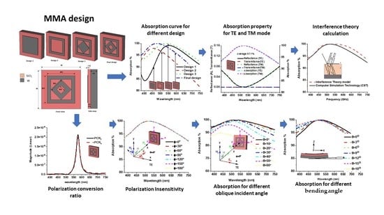
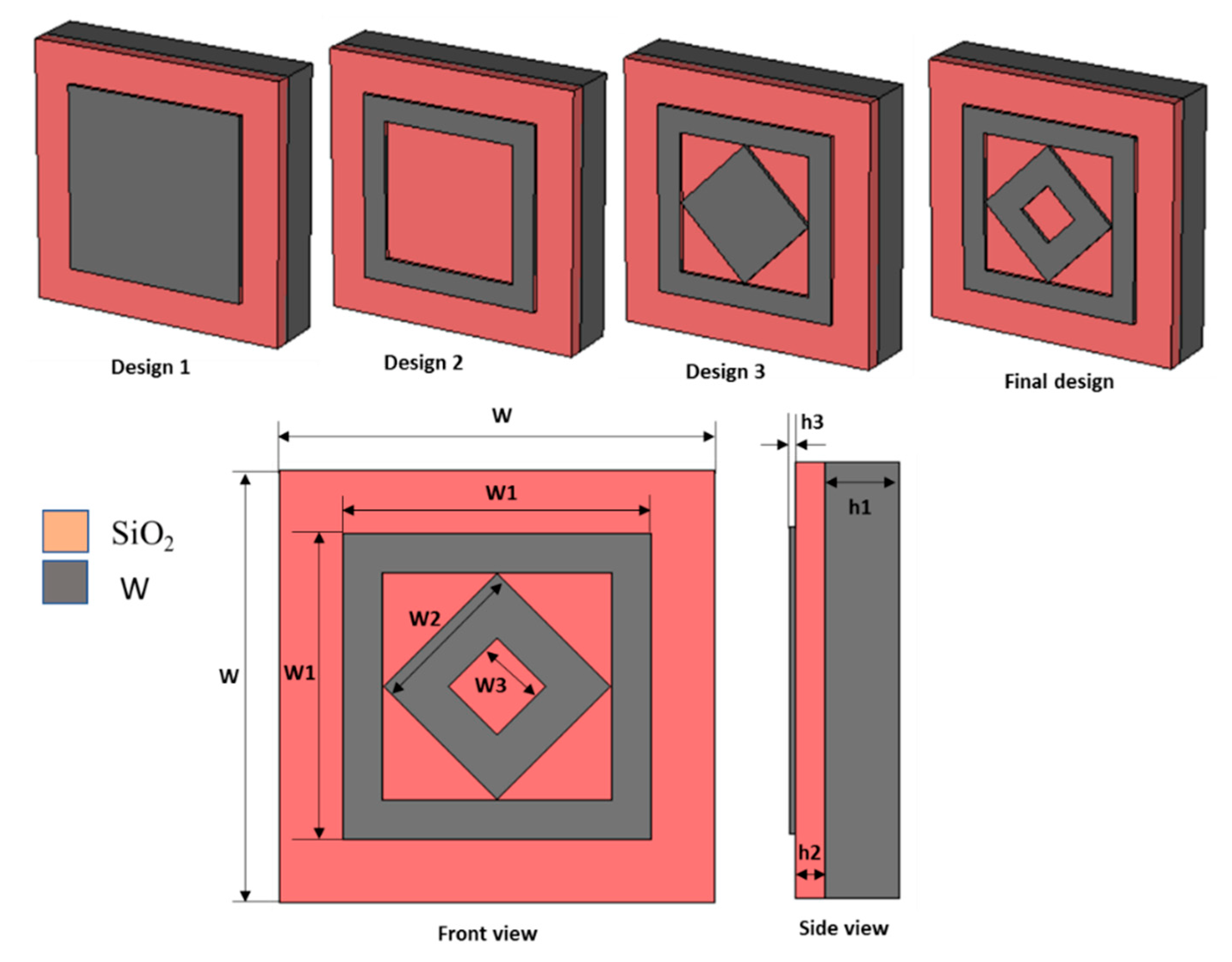
2. Absorber Design
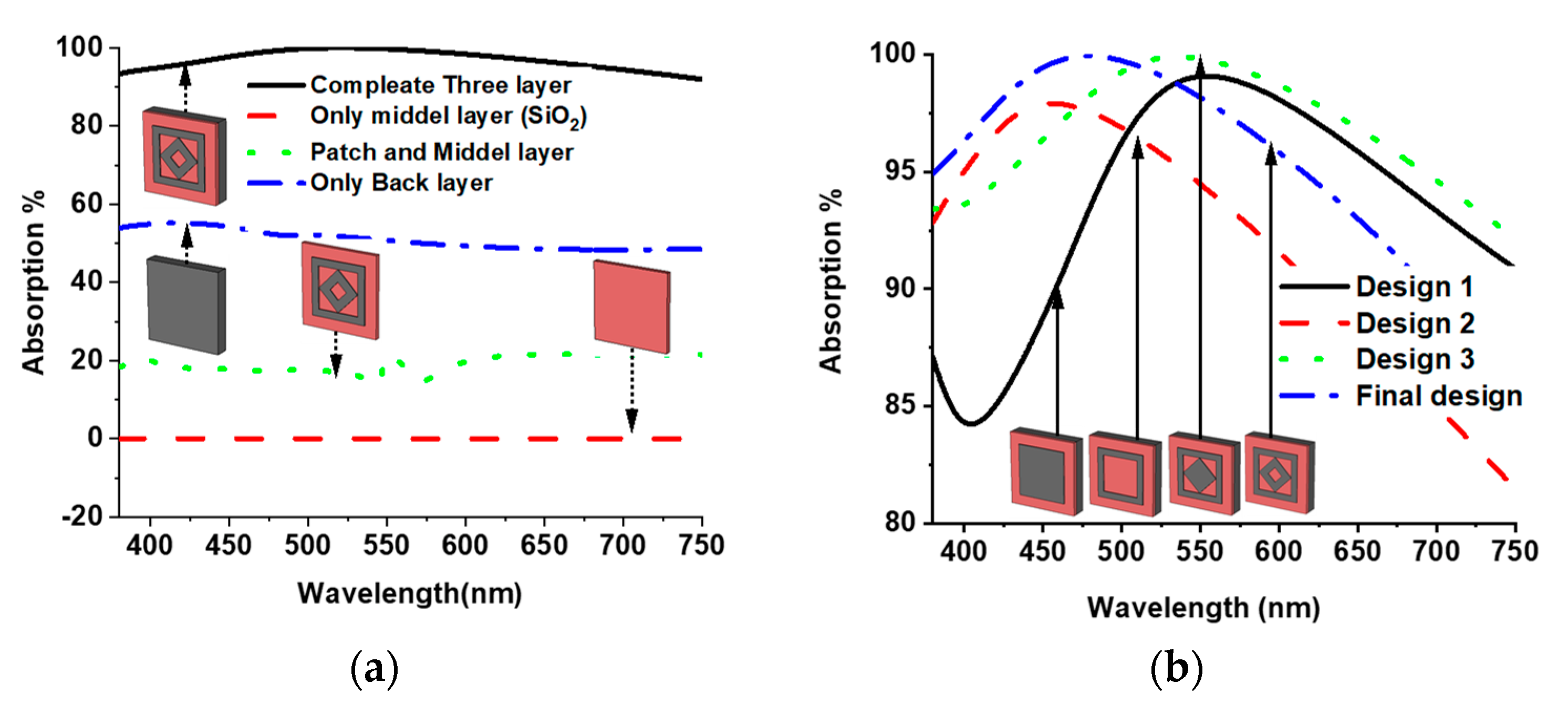
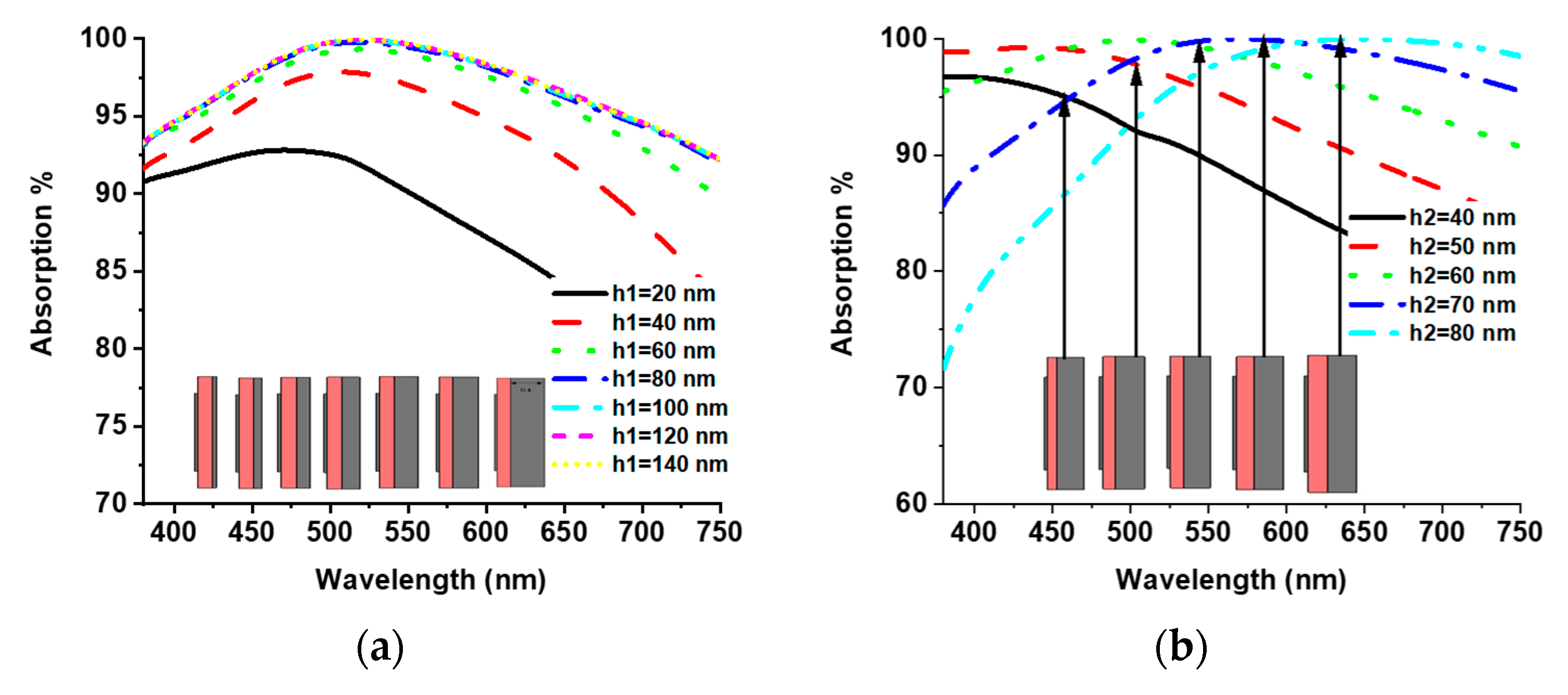
3. Results Analysis
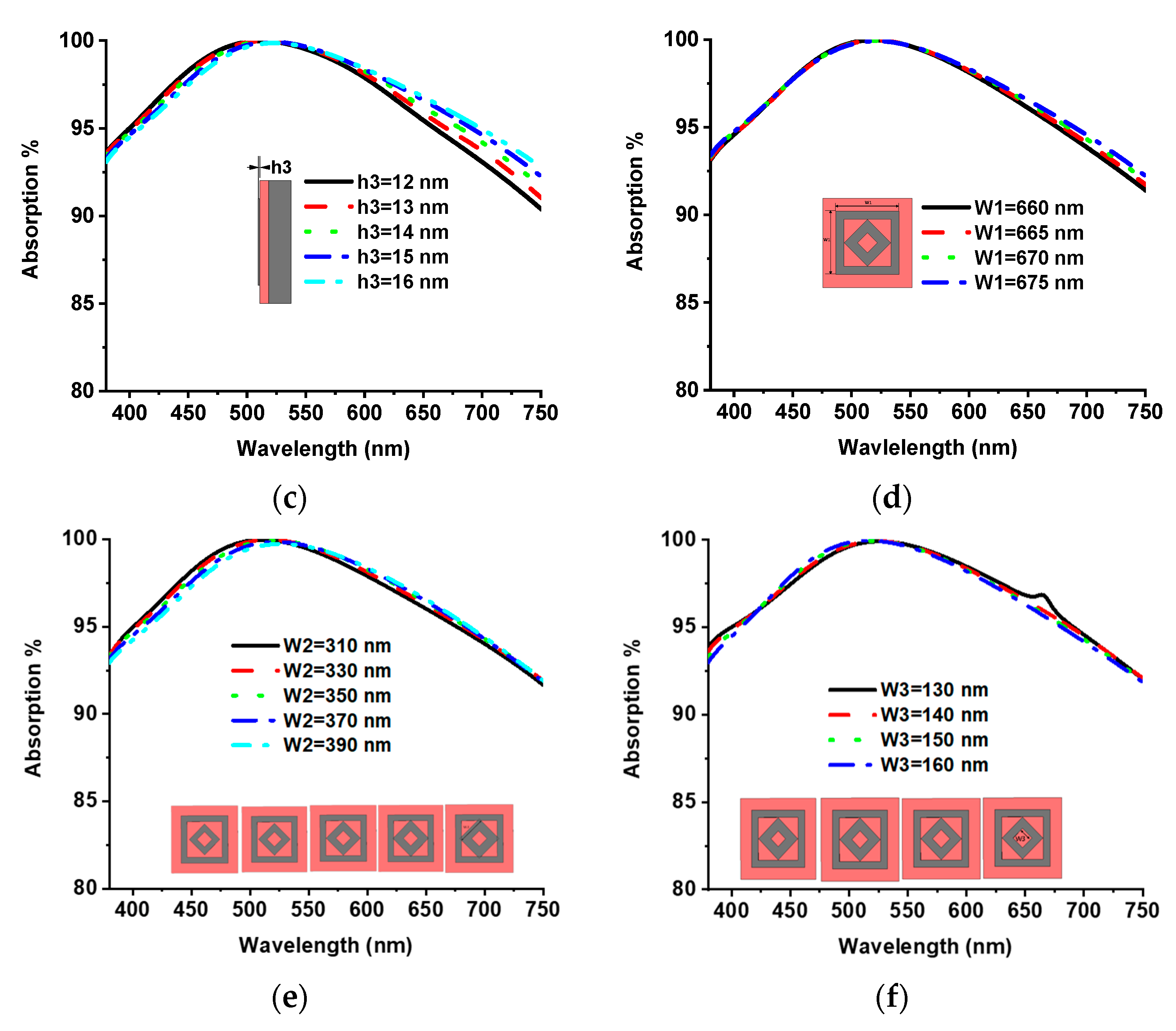
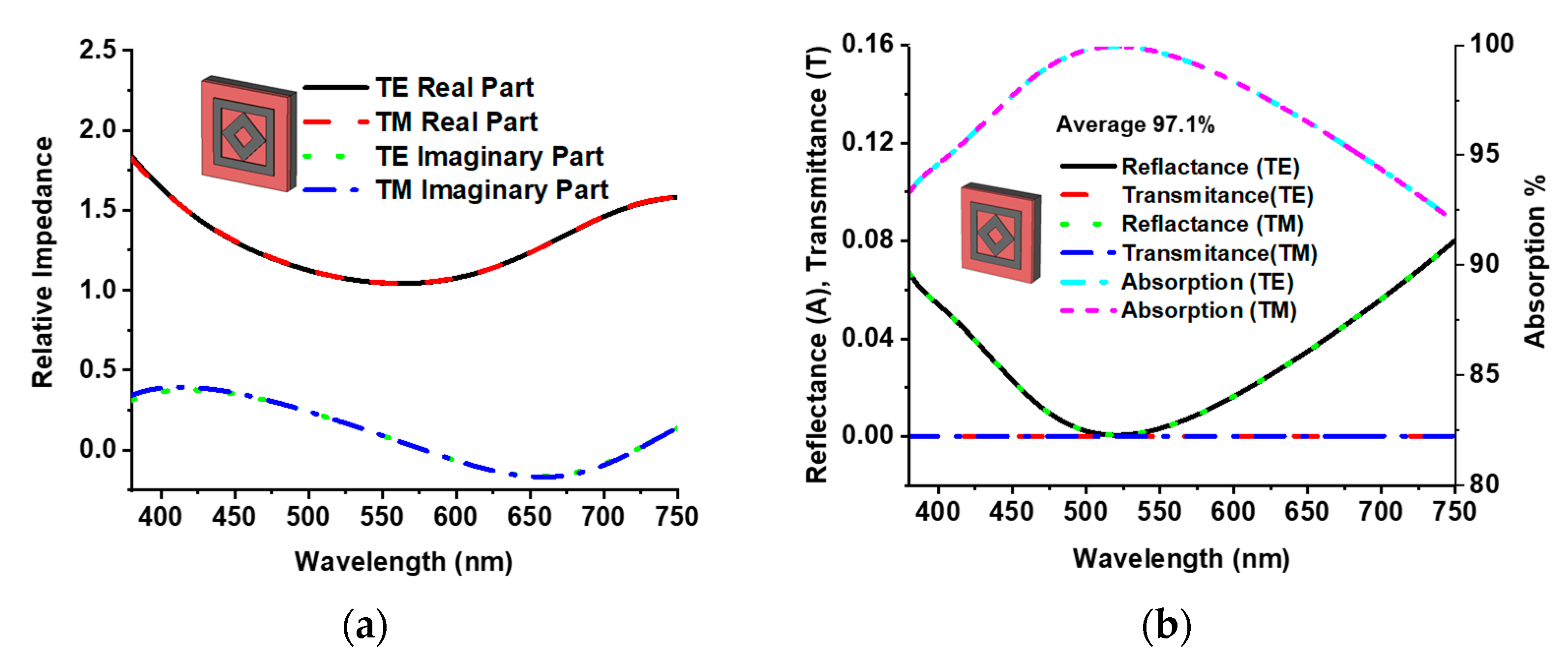
3.1. Absorption Characteristics
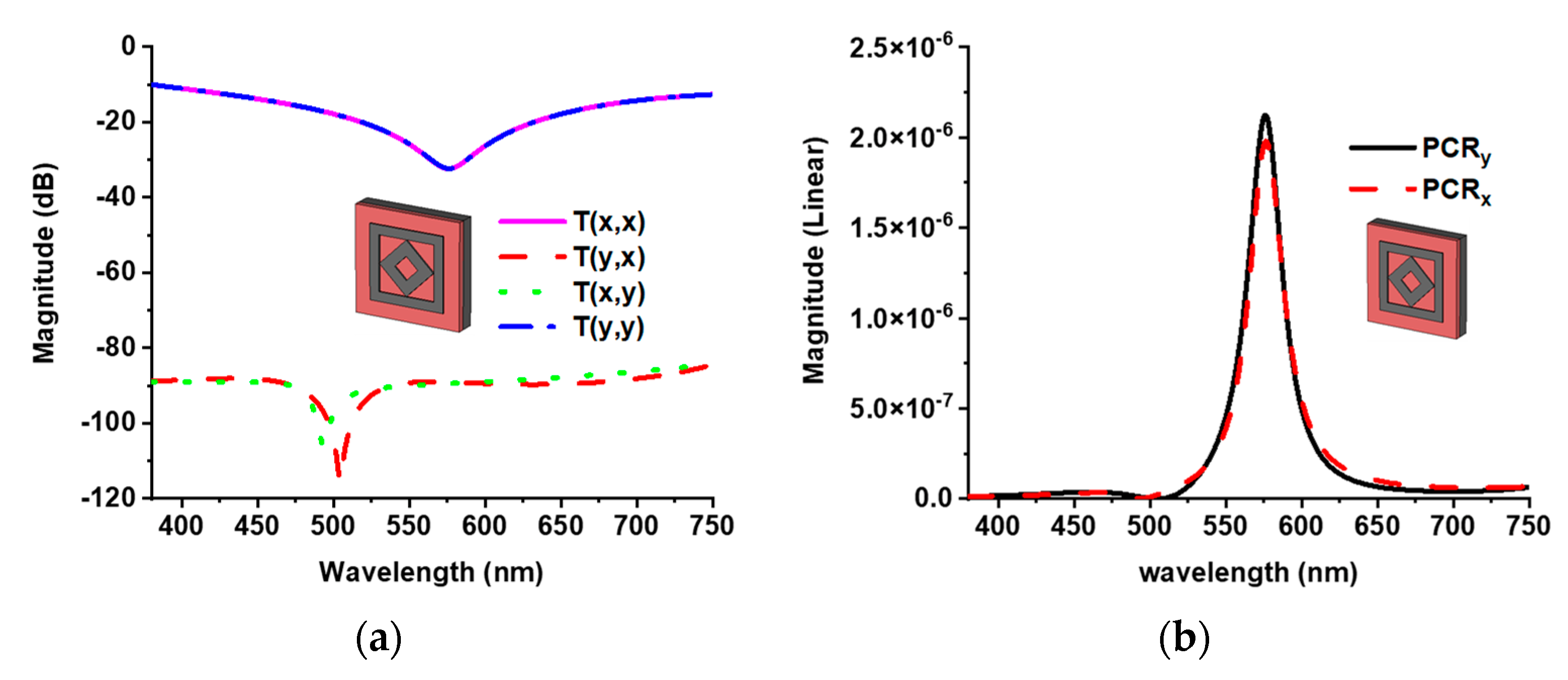
3.2. Polarization Conversion Ratio (PCR)
3.3. Metamaterial Property
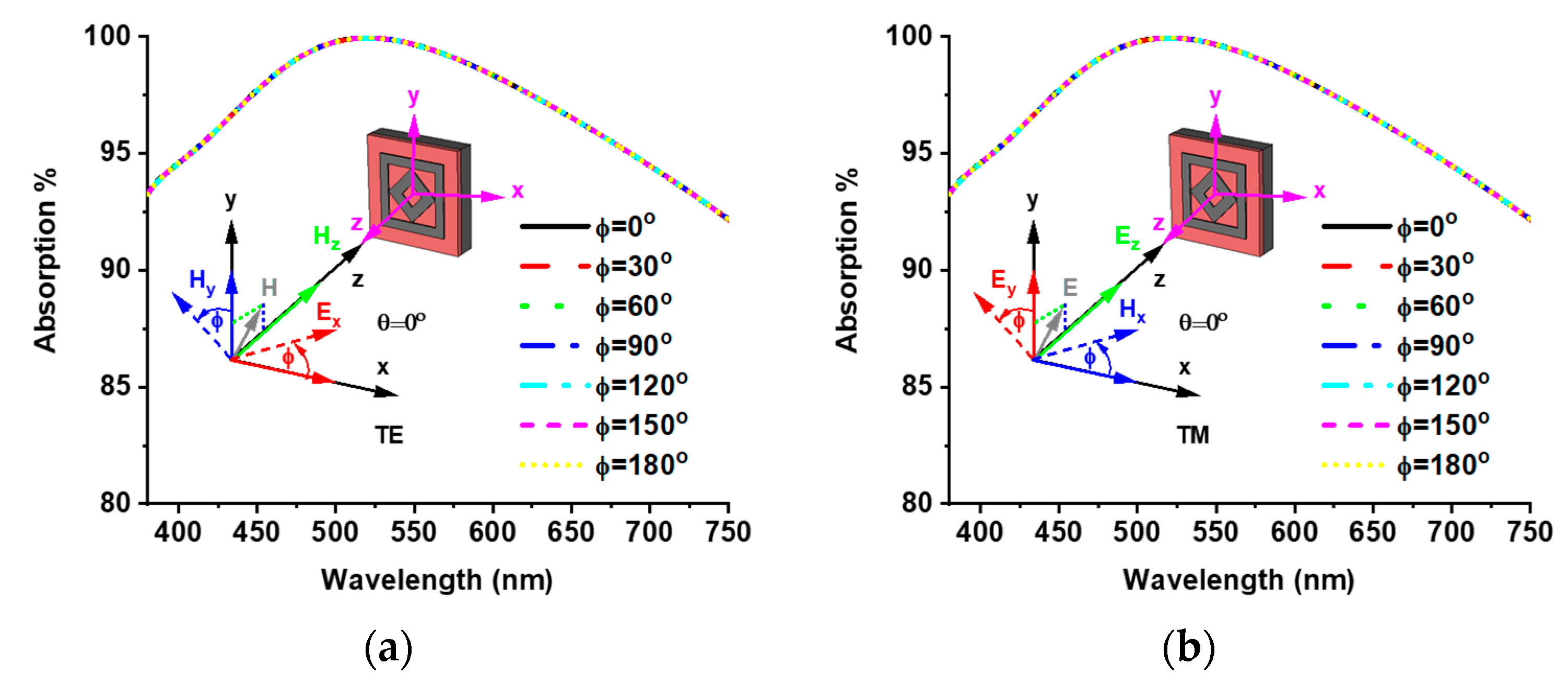
3.4. Polarization Insensitivity and Oblique Incident Angle Stability
3.5. Bendable Property
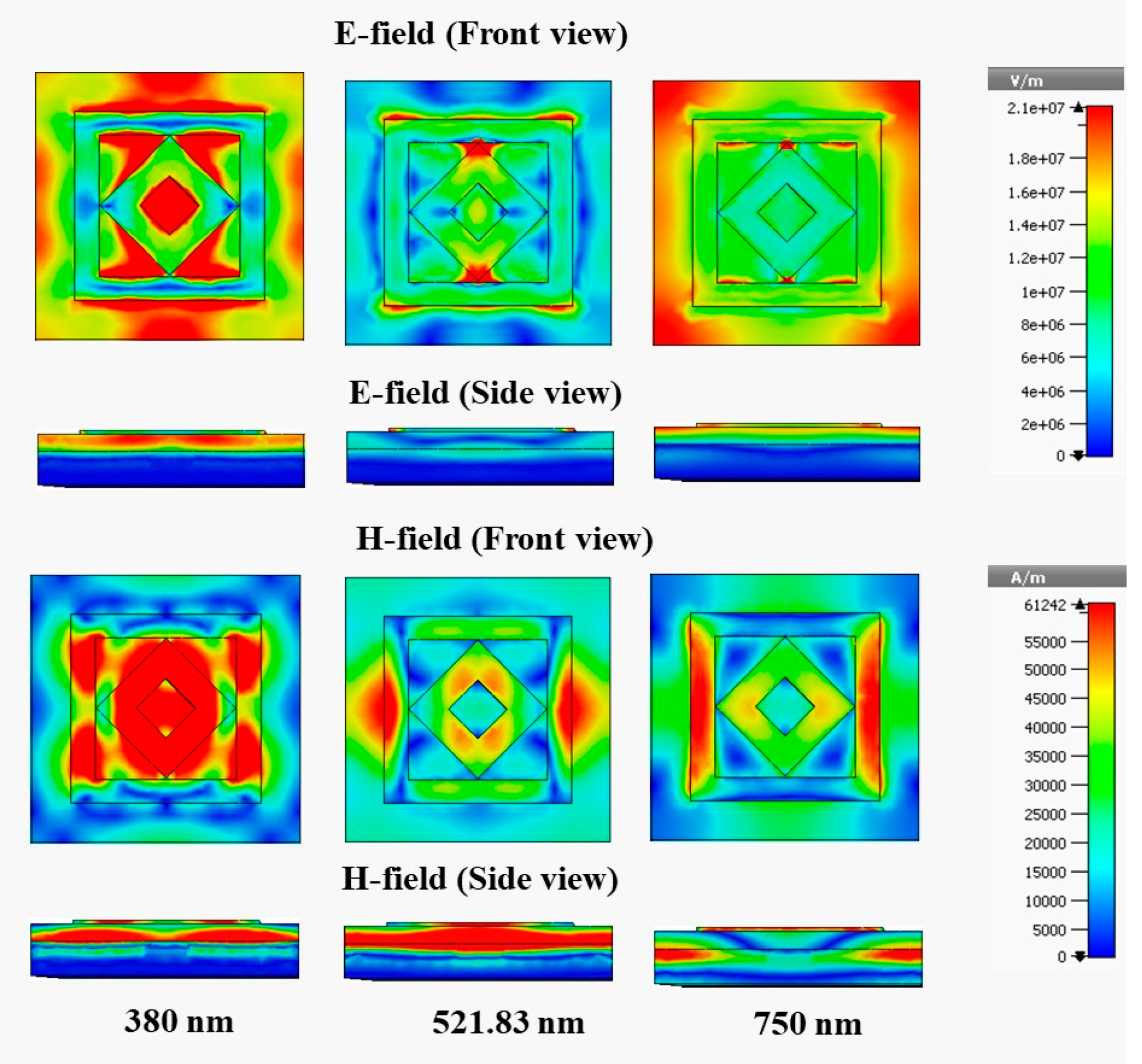
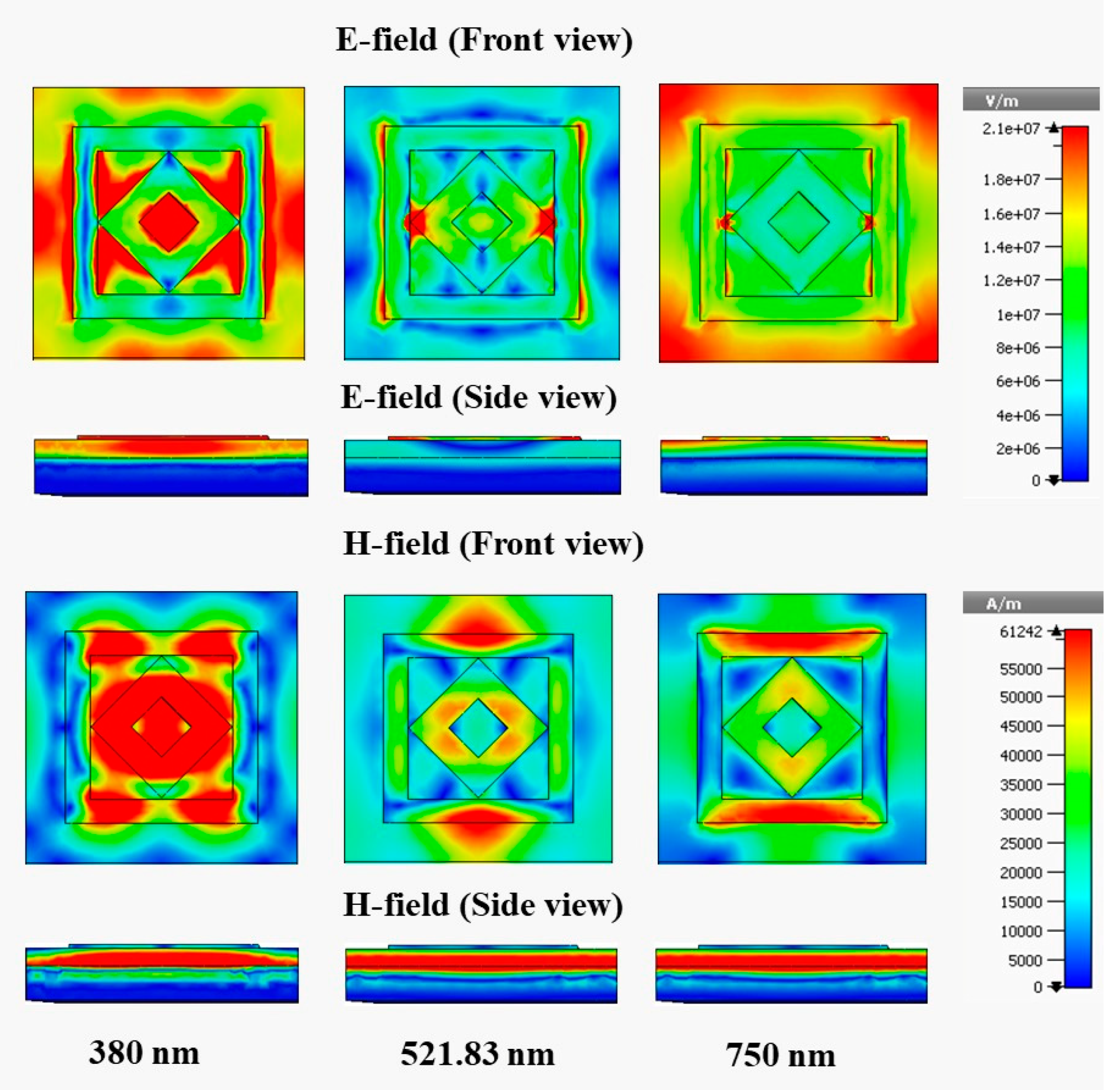
3.6. Electric and Magnetic Field
4. Conclusions
Author Contributions
Funding
Data Availability Statement
Acknowledgments
Conflicts of Interest
References
- Veselago, V.G. The Electrodynamics of Substances with Simultaneously Negative Values of Img Align= Absmiddle Alt= ϵ Eps/Img and μ. Phys. Uspekhi 1968, 10, 509–514. [Google Scholar] [CrossRef]
- Shelby, R.A.; Smith, D.R.; Schultz, S. Experimental Verification of a Negative Index of Refraction. Science 2001, 292, 77–79. [Google Scholar] [CrossRef] [PubMed] [Green Version]
- Liu, J.; Ma, W.-Z.; Chen, W.; Chen, Y.-S.; Deng, X.-C.; Gu, Y. A Metamaterial Absorber Based on Particle Swarm Optimization Suitable for Earth’s Atmospheric Transparency Window. IEEE Access 2021, 9, 92941–92951. [Google Scholar] [CrossRef]
- Ren, Z.; Liu, R.; Zhang, Y.; Lu, H.; Li, F.; Liu, Y.; Hong, X.; Guo, Y. Transmission reflection selective ultranarrow-band metamaterial filter based on electromagnetically induced transparency structure. Opt. Commun. 2021, 497, 127159. [Google Scholar] [CrossRef]
- Alam, T.; Almutairi, A.F.; Samsuzzaman, M.; Cho, M.; Islam, M.T. Metamaterial array based meander line planar antenna for cube satellite communication. Sci. Rep. 2021, 11, 14087. [Google Scholar] [CrossRef] [PubMed]
- Lee, Y.U.; Posner, C.; Zhao, J.; Zhang, J.; Liu, Z. Imaging of Cell Morphology Changes via Metamaterial-Assisted Photobleaching Microscopy. Nano Lett. 2021, 21, 1716–1721. [Google Scholar] [CrossRef] [PubMed]
- Dash, R.; Sahu, S.; Mishra, C.; Sethi, K.; Palai, G.; Sahu, S. Realization of ‘non-linear invisibility cloak’ using meta-material. Optik 2016, 127, 9635–9639. [Google Scholar] [CrossRef]
- Hakim, M.L.; Alam, T.; Almutairi, A.F.; Mansor, M.F.; Islam, M.T. Polarization insensitivity characterization of dual-band perfect metamaterial absorber for K band sensing applications. Sci. Rep. 2021, 11, 17829. [Google Scholar] [CrossRef]
- Yu, F.-Y.; Shang, X.-J.; Fang, W.; Zhang, Q.-Q.; Wu, Y.; Zhao, W.; Liu, J.-F.; Song, Q.-Q.; Wang, C.; Zhu, J.-B.; et al. A Terahertz Tunable Metamaterial Reflective Polarization Converter Based on Vanadium Oxide Film. Plasmonics 2022, 1–7. [Google Scholar] [CrossRef]
- Tang, W.; Chen, J.; Cui, T.J. Metamaterial Lenses and Their Applications at Microwave Frequencies. Adv. Photon. Res. 2021, 2, 2100001. [Google Scholar] [CrossRef]
- Landy, N.I.; Sajuyigbe, S.; Mock, J.J.; Smith, D.R.; Padilla, W.J. Perfect metamaterial absorber. Phys. Rev. Lett. 2008, 100, 207402. [Google Scholar] [CrossRef] [PubMed]
- Qiu, Y.; Zhang, P.; Li, Q.; Zhang, Y.; Li, W. A perfect selective metamaterial absorber for high-temperature solar energy harvesting. Sol. Energy 2021, 230, 1165–1174. [Google Scholar] [CrossRef]
- Hamdy, H.; Abdel-Latif, G.Y.; El-Agamy, M.; El-Mikati, H.A.; Hameed, M.F.O.; Obayya, S.S.A. Wavelength-selective metamaterial absorber based on 2D split rhombus grating for thermophotovoltic solar cell. Opt. Quantum Electron. 2022, 54, 117. [Google Scholar] [CrossRef]
- Devine, E.P. Mid-infrared photodetector based on 2D material metamaterial with negative index properties for a wide range of angles near vertical illumination. Appl. Phys. A 2021, 127, 209. [Google Scholar] [CrossRef]
- Cao, T.; Lian, M.; Lou, X.; Liu, K.; Guo, Y.; Guo, D. Wideband mid-infrared thermal emitter based on stacked nanocavity metasurfaces. Int. J. Extreme Manuf. 2021, 4, 015402. [Google Scholar] [CrossRef]
- Huang, L.; Chen, H.-T. A brief review on terahertz metamaterial perfect absorbers. Terahertz Sci. Technol. 2013, 6, 26–39. [Google Scholar]
- Zhu, W. Electromagnetic Metamaterial Absorbers: From Narrowband to Broadband. In Metamaterials and Metasurfaces; IntechOpen: London, UK, 2019. [Google Scholar] [CrossRef] [Green Version]
- Mulla, B.; Sabah, C. Perfect metamaterial absorber design for solar cell applications. Waves Random Complex Media 2015, 25, 382–392. [Google Scholar] [CrossRef]
- Ferraro, A.; Lio, G.E.; Hmina, A.; Palermo, G.; Djouda, J.M.; Maurer, T.; Caputo, R. Tailoring of plasmonic functionalized metastructures to enhance local heating release. Nanophotonics 2021, 10, 3907–3916. [Google Scholar] [CrossRef]
- Lio, G.E.; Ferraro, A.; Giocondo, M.; Caputo, R.; De Luca, A. Color Gamut Behavior in Epsilon Near-Zero Nanocavities during Propagation of Gap Surface Plasmons. Adv. Opt. Mater. 2020, 8, 2000487. [Google Scholar] [CrossRef]
- Hossain, M.J.; Faruque, M.R.I.; Ahmed, R.; Alam, J.; Islam, M.T. Polarization-insensitive infrared-visible perfect metamaterial absorber and permittivity sensor. Results Phys. 2019, 14, 102429. [Google Scholar] [CrossRef]
- Mahmud, S.; Islam, S.S.; Mat, K.; Chowdhury, M.E.H.; Rmili, H.; Islam, M.T. Design and parametric analysis of a wide-angle polarization-insensitive metamaterial absorber with a star shape resonator for optical wavelength applications. Results Phys. 2020, 18, 103259. [Google Scholar] [CrossRef]
- Zhu, P.; Guo, L.J. High performance broadband absorber in the visible band by engineered dispersion and geometry of a metal-dielectric-metal stack. Appl. Phys. Lett. 2012, 101, 241116. [Google Scholar] [CrossRef]
- Liu, Z.; Liu, X.; Huang, S.; Pan, P.; Chen, J.; Liu, G.; Gu, G. Automatically Acquired Broadband Plasmonic-Metamaterial Black Absorber during the Metallic Film-Formation. ACS Appl. Mater. Interfaces 2015, 7, 4962–4968. [Google Scholar] [CrossRef] [PubMed]
- Butun, S.; Aydin, K. Structurally tunable resonant absorption bands in ultrathin broadband plasmonic absorbers. Opt. Express 2014, 22, 19457–19468. [Google Scholar] [CrossRef] [PubMed] [Green Version]
- Hoa, N.T.Q.; Tung, P.D.; Lam, P.H.; Dung, N.D.; Quang, N.H. Numerical Study of an Ultrabroadband, Wide-Angle, Polarization-Insensitivity Metamaterial Absorber in the Visible Region. J. Electron. Mater. 2018, 47, 2634–2639. [Google Scholar] [CrossRef]
- Luo, M.; Shen, S.; Zhou, L.; Wu, S.; Zhou, Y.; Chen, L. Broadband, wide-angle, and polarization-independent metamaterial absorber for the visible regime. Opt. Express 2017, 25, 16715–16724. [Google Scholar] [CrossRef]
- Ghosh, G. Dispersion-equation coefficients for the refractive index and birefringence of calcite and quartz crystals. Opt. Commun. 1999, 163, 95–102. [Google Scholar] [CrossRef]
- Ding, J.; Feng, A.; Li, X.; Ding, S.; Liu, L.; Ren, W. Properties, preparation, and application of tungsten disulfide: A review. J. Phys. D Appl. Phys. 2021, 54, 173002. [Google Scholar] [CrossRef]
- Kanmaz, I.; Abdullah, Ü. Silicon dioxide thin films prepared by spin coating for the application of solar cells. Int. Adv. Res. Eng. J. 2021, 5, 14–18. [Google Scholar] [CrossRef]
- AGDC. CST Studio Suite. 2019. Available online: https://www.3ds.com/products-services/simulia/products/cst-studio-suite/ (accessed on 22 January 2022).
- Cen, C.; Chen, Z.; Xu, D.; Jiang, L.; Chen, X.; Yi, Z.; Wu, P.; Li, G.; Yi, Y. High quality factor, high sensitivity metamaterial graphene—Perfect absorber based on critical coupling theory and impedance matching. Nanomaterials 2020, 10, 95. [Google Scholar] [CrossRef] [PubMed] [Green Version]
- Hakim, M.L.; Alam, T.; Soliman, M.S.; Sahar, N.M.; Baharuddin, M.H.; Almalki, S.H.A.; Islam, M.T. Polarization insensitive symmetrical structured double negative (DNG) metamaterial absorber for Ku-band sensing applications. Sci. Rep. 2022, 12, 479. [Google Scholar] [CrossRef] [PubMed]
- Mahmud, S.; Karim, M.; Islam, S.S.; Shuvo, M.K.; Akter, T.; Almutairi, A.F.; Islam, M.T. A Multi-Band Near Perfect Polarization and Angular Insensitive Metamaterial Absorber With a Simple Octagonal Resonator for Visible Wavelength. IEEE Access 2021, 9, 117746–117760. [Google Scholar] [CrossRef]
- Xiao, Z.-Y.; Liu, D.-J.; Ma, X.-L.; Wang, Z.-H. Multi-band transmissions of chiral metamaterials based on Fabry-Perot like resonators. Opt. Express 2015, 23, 7053–7061. [Google Scholar] [CrossRef] [PubMed]
- Deng, B.; Xu, R.; Zhao, K.; Lu, Y.; Ganguli, S.; Cheng, G.J. Composite bending-dominated hollow nanolattices: A stiff, cyclable mechanical metamaterial. Mater. Today 2018, 21, 467–474. [Google Scholar] [CrossRef] [Green Version]


| Parameters | h1 | h2 | h3 | W | W1 | W2 | W3 |
|---|---|---|---|---|---|---|---|
| Value (nm) | 120 | 62.82 | 15 | 950 | 670 | 350 | 150 |
| Theta (θ) | TE Mode Absorption | TM Mode Absorption | ||
|---|---|---|---|---|
| Average | Peak | Average | Peak | |
| 0° | 97.12% | 99.99% | 97.10% | 99.99% |
| 10° | 97.07% | 99.93% | 97.07% | 99.96% |
| 20° | 96.86% | 99.70% | 97.29% | 99.99% |
| 30° | 96.02% | 99.32% | 97.51% | 99.96% |
| 40° | 93.76% | 98.60% | 97.54% | 99.70% |
| 50° | 90.61% | 96.09% | 96.81% | 98.98% |
| 60° | 84.43% | 89.61% | 94.32% | 96.64% |
| 70° | 70% | 76.25% | 86.41% | 89.17% |
| Ref. | Material | Size (mm) | Operation Range | Bandwidth (nm) | Polarization Insensitivity | Incident Angle Stability A ≥ 70% | Absorption | Peak Absorption |
|---|---|---|---|---|---|---|---|---|
| [23] | Cu, Si3N4, Si | N/A | 400–700 | 380 | No | N/A | 80% | 97% |
| [24] | Au, SiO2 | 600 × 600 × 180 | 370–880 | 510 | No | N/A | 83% | 92% |
| [25] | Ag, SiO2 | 350 × 350 × 180 | 400–700 | 300 | No | N/A | 80% | 98% |
| [22] | W. SiO2 | 1000 × 1000 × 225 | 389.34–697.19 | 307.85 | Yes | 60° | 91.24% | 99.9% |
| [26] | Au, Si | 500 × 500 × 600 | 474.4–784.4 | 310 | Yes | 65° | 80% | 98.5% |
| [27] | Ni, Si | 250 × 250 × 355 | 400–700 | 300 | Yes | 60° | 90% | 99% |
| Proposed | W. SiO2 | 950 × 950 × 240.13 | 380–750 | 370 | Yes | 70° | 92.2% | 99.99% |
Publisher’s Note: MDPI stays neutral with regard to jurisdictional claims in published maps and institutional affiliations. |
© 2022 by the authors. Licensee MDPI, Basel, Switzerland. This article is an open access article distributed under the terms and conditions of the Creative Commons Attribution (CC BY) license (https://creativecommons.org/licenses/by/4.0/).
Share and Cite
Hakim, M.L.; Alam, T.; Islam, M.S.; Salaheldeen M., M.; Almalki, S.H.A.; Baharuddin, M.H.; Alsaif, H.; Islam, M.T. Wide-Oblique-Incident-Angle Stable Polarization-Insensitive Ultra-Wideband Metamaterial Perfect Absorber for Visible Optical Wavelength Applications. Materials 2022, 15, 2201. https://doi.org/10.3390/ma15062201
Hakim ML, Alam T, Islam MS, Salaheldeen M. M, Almalki SHA, Baharuddin MH, Alsaif H, Islam MT. Wide-Oblique-Incident-Angle Stable Polarization-Insensitive Ultra-Wideband Metamaterial Perfect Absorber for Visible Optical Wavelength Applications. Materials. 2022; 15(6):2201. https://doi.org/10.3390/ma15062201
Chicago/Turabian StyleHakim, Mohammad Lutful, Touhidul Alam, Md. Shabiul Islam, M. Salaheldeen M., Sami H. A. Almalki, Mohd Hafiz Baharuddin, Haitham Alsaif, and Mohammad Tariqul Islam. 2022. "Wide-Oblique-Incident-Angle Stable Polarization-Insensitive Ultra-Wideband Metamaterial Perfect Absorber for Visible Optical Wavelength Applications" Materials 15, no. 6: 2201. https://doi.org/10.3390/ma15062201
APA StyleHakim, M. L., Alam, T., Islam, M. S., Salaheldeen M., M., Almalki, S. H. A., Baharuddin, M. H., Alsaif, H., & Islam, M. T. (2022). Wide-Oblique-Incident-Angle Stable Polarization-Insensitive Ultra-Wideband Metamaterial Perfect Absorber for Visible Optical Wavelength Applications. Materials, 15(6), 2201. https://doi.org/10.3390/ma15062201