Article

Impact of Cesium Concentration on Optoelectronic Properties of Metal Halide Perovskites

by
Steponas Ašmontas
*,
Aurimas Čerškus
,
Jonas Gradauskas
,
Asta Grigucevičienė
,
Remigijus Juškėnas
,
Konstantinas Leinartas
,
Andžej Lučun
,
Kazimieras Petrauskas
,
Algirdas Selskis
,
Algirdas Sužiedėlis
and
Edmundas Širmulis
Center for Physical Sciences and Technology, Savanorių Ave. 231, LT-02300 Vilnius, Lithuania
*
Author to whom correspondence should be addressed.
Materials 2022, 15(5), 1936; https://doi.org/10.3390/ma15051936
Submission received: 18 January 2022 / Revised: 22 February 2022 / Accepted: 1 March 2022 / Published: 4 March 2022
(This article belongs to the Special Issue Emerging Photovoltaic Materials and Solar Cells)

Abstract

:
Performance of a perovskite solar cell is largely influenced by the optoelectronic properties of metal halide perovskite films. Here we study the influence of cesium concentration on morphology, crystal structure, photoluminescence and optical properties of the triple cation perovskite film. Incorporation of small amount (x = 0.1) of cesium cations into Csx(MA0.17FA0.83)1−x Pb(I0.83Br0.17)3 leads to enhanced power conversion efficiency (PCE) of the solar cell resulting mainly from significant rise of the short-current density and the fill factor value. Further increase of Cs concentration (x > 0.1) decreases the film’s phase purity, carrier lifetime and correspondingly reduces PCE of the solar cell. Higher concentration of Cs (x ≥ 0.2) causes phase segregation of the perovskite alongside with formation of Cs-rich regions impeding light absorption.

1. Introduction

Metal halide perovskites attract considerable attention due to their remarkable properties revealing potential applications in optoelectronic devices such as solar cells [1,2,3,4,5,6,7,8,9,10,11,12,13], photodetectors [14,15,16,17,18,19,20,21,22,23], light emitting diodes [24,25,26,27,28,29,30,31,32,33,34]. They have also been used for photocatalysts [35] and bioimaging [36]. In solar cells, metal halide perovskites are attractive for their unique features such as high value of the absorption coefficient across the entire visible spectrum range that allows to use a thin perovskite film [37,38], high defect tolerance [39], high carrier mobility [40,41], and long carrier diffusion length [42,43]. Possibility of fine band gap tuning allows using perovskite layer as a top sub-cell in a tandem solar cell [44,45,46]. The methylammonium (MA) based metal halide perovskite has been the pioneer in this class of materials. However, MA cation-based metal halide perovskites suffer from inherently high instability when exposed to heat or moisture [8,12]. It was shown that degradation of MAPbI3 perovskites caused by illumination or elevated temperatures is typically triggered by the volatilization of the MA cation [12]. In search of stable perovskite crystal, cesium [47] or formamidinium (FA) was used in combination with the MA cation [44,47,48]. At present, the best quality demonstrating solar cells use a mixture of (FA) and (MA) as the monovalent cations [48,49,50,51,52,53,54]. Addition of cesium makes the triple cation perovskite composition thermally more stable as far as it has less phase impurities and is less sensitive to processing conditions [48,55,56]. It is shown that incorporation of small amount of Cs reduces the trap density and charge recombination rate in the perovskite layers [57]. Thus, performance of the double cation perovskite solar cells can be improved by means of adding a small amount of Cs cations [49,56,57,58,59]. Addition of Cs also enhanced the quality of formamidinium lead iodide perovskite solar cells; this gain was explained by the improved crystallinity which is linked to stabilization of the photoactive perovskite layer by suppressing the phase transition into the yellow nonperovskite structure at room temperature [59,60,61,62]. Rehman et al. demonstrated that charge carrier mobility and lifetime were increased substantially due to addition of Cs into the mixed-cation lead mixed-halide perovskite CsxFA1−x Pb(I0.6Br0.4)3 film in relative content of Cs up to x = 0.2, and then was followed by a plunge of these parameters to much lower values in the content range of 0.3 < x < 0.8 [61]. Since the mixture of (FA) and (MA) perovskite layers is widely used as a top sub-cell in the tandem solar cells [45,46,47,48,49,63,64,65,66,67,68,69,70,71,72,73,74], it is essential to understand the impact of cesium cation additive on perovskite’s optoelectronic properties aiming at improved performance of tandem solar cells.
In this work, we present the results of experimental study of optical, photoluminescence and charge transport properties of perovskite Csx(MA0.17FA0.83)1−x Pb(I0.83Br0.17)3 layers containing different cesium concentration (0 ≤ x ≤ 0.6). The transient photovoltage and photoelectric characteristics of the perovskite solar cells are reported as well.

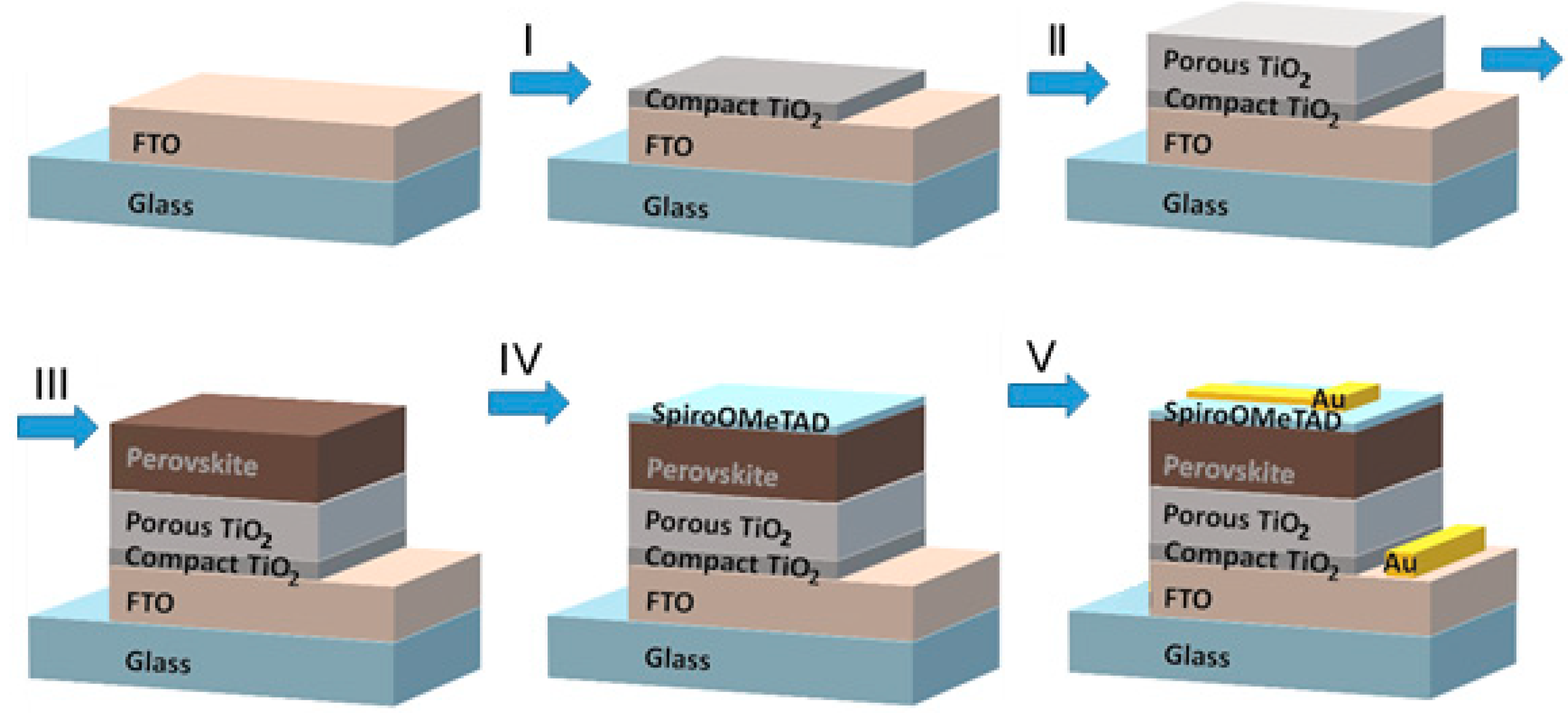
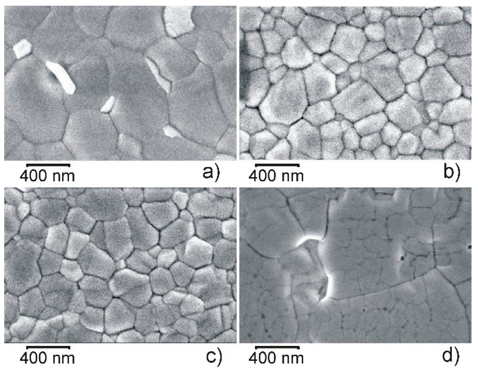
2. Fabrication of Perovskite Films and Their Characterization

In the present study, perovskite films were fabricated according to the methods described earlier [49,75,76]. All the reagents, their concentrations and purity grades, the sequence of procedures and equipment used for the fabrication of the perovskite solar cells were depicted in detail in our previous paper [58]. The triple cation perovskite films were deposited on the 25 × 25 mm2 glass substrates coated with transparent fluorine-doped tin oxide (FTO) layer (TEC 10, Ossila B.V., Sheffield, UK). Approximately 7 × 25 mm2 of the FTO coating was removed from one edge of the glass substrate using zinc powder (Sigma Aldrich, MO, USA) and hydrochloric acid (Merck KGaA, Darmstadt, Germany), followed by sonication in 2% Helmanex (Hellma GmbH&Co, Müllheim, Germany) for 20 min. Then the substrates were rinsed with deionized water and sonicated in isopropanol (Merck KGaA, Darmstadt, Germany) for 20 min before being exposed to plasma treatment for 10 min. The main steps of the perovskite solar cell formation are shown in Figure 1.
During step I, a ~30 nm-thick compact TiO2 (Greatcell Solar Italia S.R.L., Roma, Italy) layer was deposited on the FTO coating by means of spray pyrolysis of precursor solution consisting of titanium diisopropoxide (bis) acetylacetonate Ti(acac)2OiPr2 (Merck KGaA, Darmstadt, Germany) and anhydrous ethanol (Sigma Aldrich, MO, USA) (1:9 volume ratio) at 450 °C followed by annealing for 15 min. After the deposition, the structures were allowed to cool down to room temperature. During step II, mesoporous TiO2 layer was formed by spin coating of 180 µL of suspension containing titanium oxide nanoparticles (30 nm) diluted in ethanol (1:6 weight ratio) at 4000 rpm for 20 s with an acceleration of 2000 rpm·s−2. Then the substrates were annealed at 450 °C for 30 min. After cooling down, they were transferred to a nitrogen-filled glove-box (M. Braun Inertgas-Systeme GMBH, Garching bei München, Germany). During step III, the perovskite layer was deposited from a freshly prepared solution of 1.2 M lead iodide (Sigma Aldrich, MO, USA), 0.2 M methylammonium bromide (Greatcell Solar Italia S.R.L., Roma, Italy), 0.2 M lead bromide (Sigma Aldrich, MO, USA) and 1 M formamidinium iodide (Greatcell Solar Italia S.R.L., Roma, Italy). The mixture of anhydrous N,N-dimethylformamide (Sigma Aldrich, MO, USA), and dimethylsulfoxide (DMF/DMSO) (Sigma Aldrich, MO, USA) with volume ratio of 4:1 was used as a solvent. The content of cesium ions in the perovskite layer was varied by means of choosing CsI (Strem Chemicals INC MS, IL, USA) (1.5 M of CsI in DMSO) concentration from 0 to 60%. The prepared precursor solution was spin coated by a two-step program: the first was at 1000 rpm for 10 s, and the second was at 6000 rpm for 30 s. Approximately 10 s prior to the end of the spinning, 150 µL of chlorobenzene (Sigma Aldrich, MO, USA) was dropped onto the top surface and annealed at 100 °C for 60 min. The fourth step of the cell fabrication was up for formation of the hole transporting layer (HTL). The HTL was formed by spinning of 150 μL of 70 mM solution of 2-N,2-N,2-N′,2-N′,7-N,7-N,7-N′,7-N′-octakis(4-methoxyphenyl)-9,9′-91 spiro-bi[fluorene]-2,2′,7,7′-tetramine (Spiro-OMeTAD) in chlorobenzene (85.78 mg/mL), supplemented with 17 μL of Li-bis((trifluoromethyl)sulfonyl)imide (Li-TFSI) salt in anhydrous acetonitrile (520 mg/mL) and 28.8 μL of 4-tert-butylpyridine (TBP) solutions just before the application (all from Sigma Aldrich, MO, USA). The molar ratio of dopants to the Spiro-OMeTAD was 0.5 and 3.3 for Li-TFSI and 4TBP, respectively. The spin-coating regime of step IV was 4000 rpm for 25 s with acceleration of 2000 rpm·s−2. During the final step V, ~70 nm-thick Au contacts (Kurt J. Lesker Company, Clairton, Germany) were deposited on top of Spiro-OMeTAD and FTO by means of thermal evaporation in the vacuum chamber of “VAKSIS PVD Vapor-5S_Th” (Vaksis R&D and Engineering, Ankara, Turkey).
Morphology and thickness of the perovskite films were examined by means of scanning electron microscope (SEM) (Helios NanoLab 650, FEI, Hillsboro, OR, USA). Chemical composition of the films was studied with the SEM-supplemented energy dispersive X-ray spectrometer (EDX) (INCA Energy, Oxford Instruments, Abingdon, UK).
Crystallographic structure of the fabricated perovskite films was investigated using X-ray diffractometer (XRD) equipped with a 9 kW power rotating Cu anode X-ray source and theta/theta goniometer (SmartLab, Rigaku, Tokyo, Japan). The patterns were measured with Bragg-Brentano geometry in 2Θ range of 10°–65°. The main features of the full-scale perovskite layers’ XRD patterns were analyzed in our previous work [55]. In this study, the detailed analysis of the fragments of XRD patterns in the 2Θ range of 10–15° was carried out.
Photoluminescence (PL) and transient PL spectra were measured at room temperature. An Ar-ion laser or diode pumped solid state (DPSS) microchip laser (Standa Ltd., Vilnius, Lithuania) were used for excitation, and a 1-m monochromator and TE-cooled PMT utilizing photon counting technique were used for data recording. More details of the technique were described in our previous paper [58]. The Ar-ion laser power density was varied over three orders of magnitude (from 63 down to 0.06 mW/cm2) and the microchip laser fluence was varied over two orders of magnitude, from 0.076 to 7.6 μJ/cm2 per pulse, with a linear variable metallic neutral density filter.
Transient photovoltage of the solar cells was investigated using 7 ns-long laser pulses of 532 nm wavelength generated at 50 Hz repetition rate by the diode pumped frequency-doubled Nd:YAG-LBO laser NL202 (Ekspla Ltd., Vilnius, Lithuania). Average power of the laser radiation was measured by optical power meter PM400 (Thorlabs Inc., Newton, NJ, USA). The transient photovoltage and the laser pulse were recorded by digital storage oscilloscope Agilent Technologies DSO6102A (Agilent Technologies Inc., Santa Clara, CA, USA), and the laser pulse shape was registered by the high-speed optical signal reference detector 11HSP-FS1 (Standa Ltd., Vilnius, Lithuania).
Absorbance spectra of the perovskite films were estimated from the optical transmission data obtained with spectrometer AvaSpec-ULS2048XL-EVO (Avantes, Apeldoorn, The Netherlands).
Keithley 2602A (Keithley Instruments Inc., Cleveland, OH, USA) equipment was used for direct measurement of current-voltage characteristics of the perovskite solar cells. The 100 mW/cm2 irradiance was achieved by an AM 1.5 spectral lamp (Newport model 67005, Newport Corp., Irvine, CA, USA) placed at an appropriate distance.

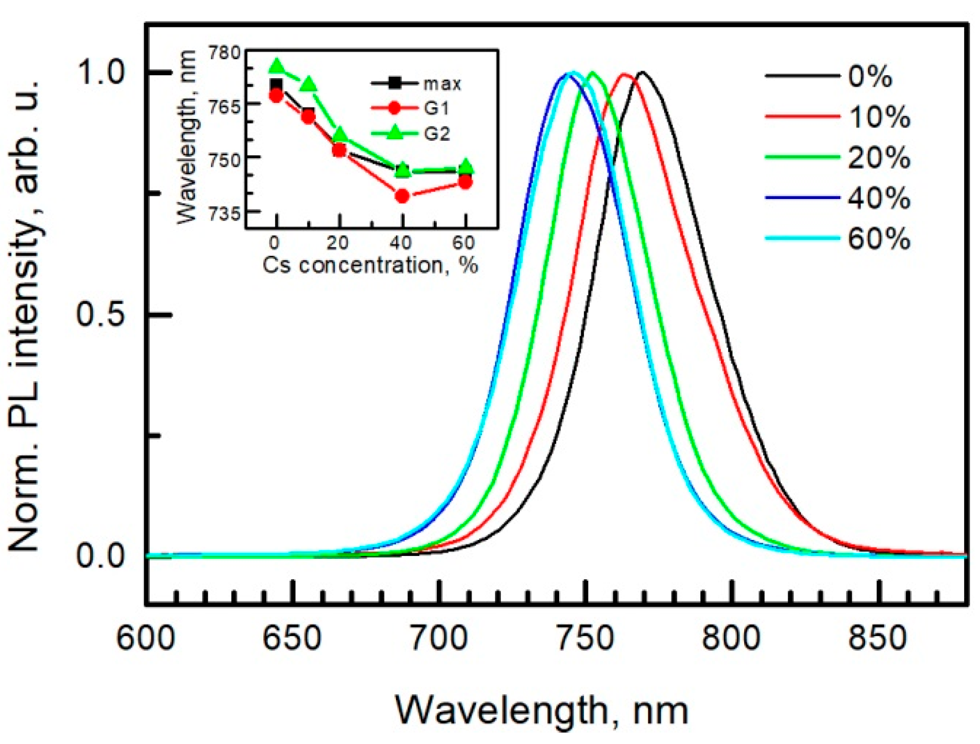
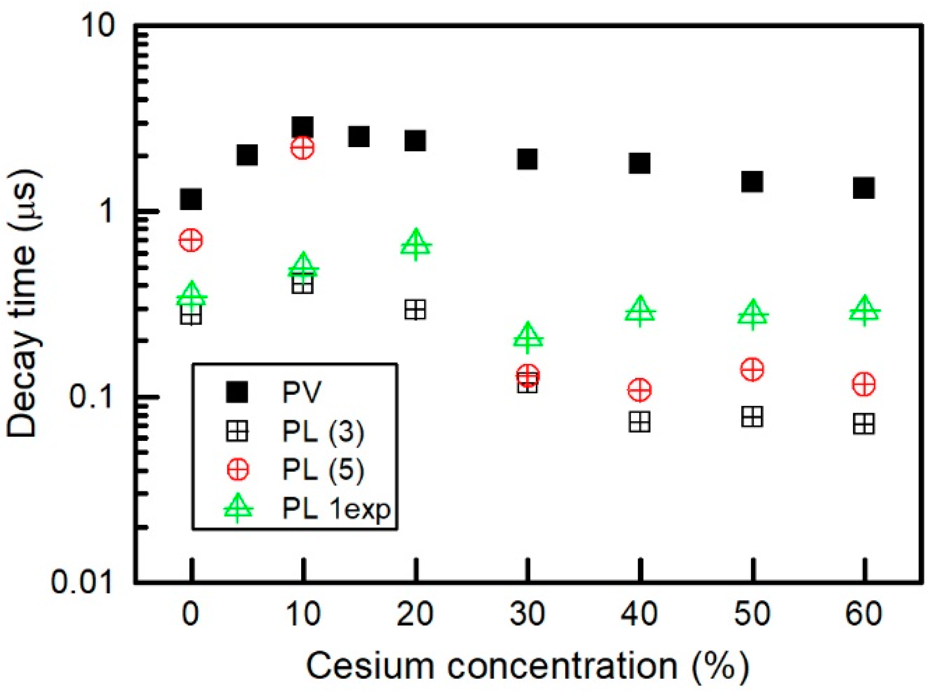
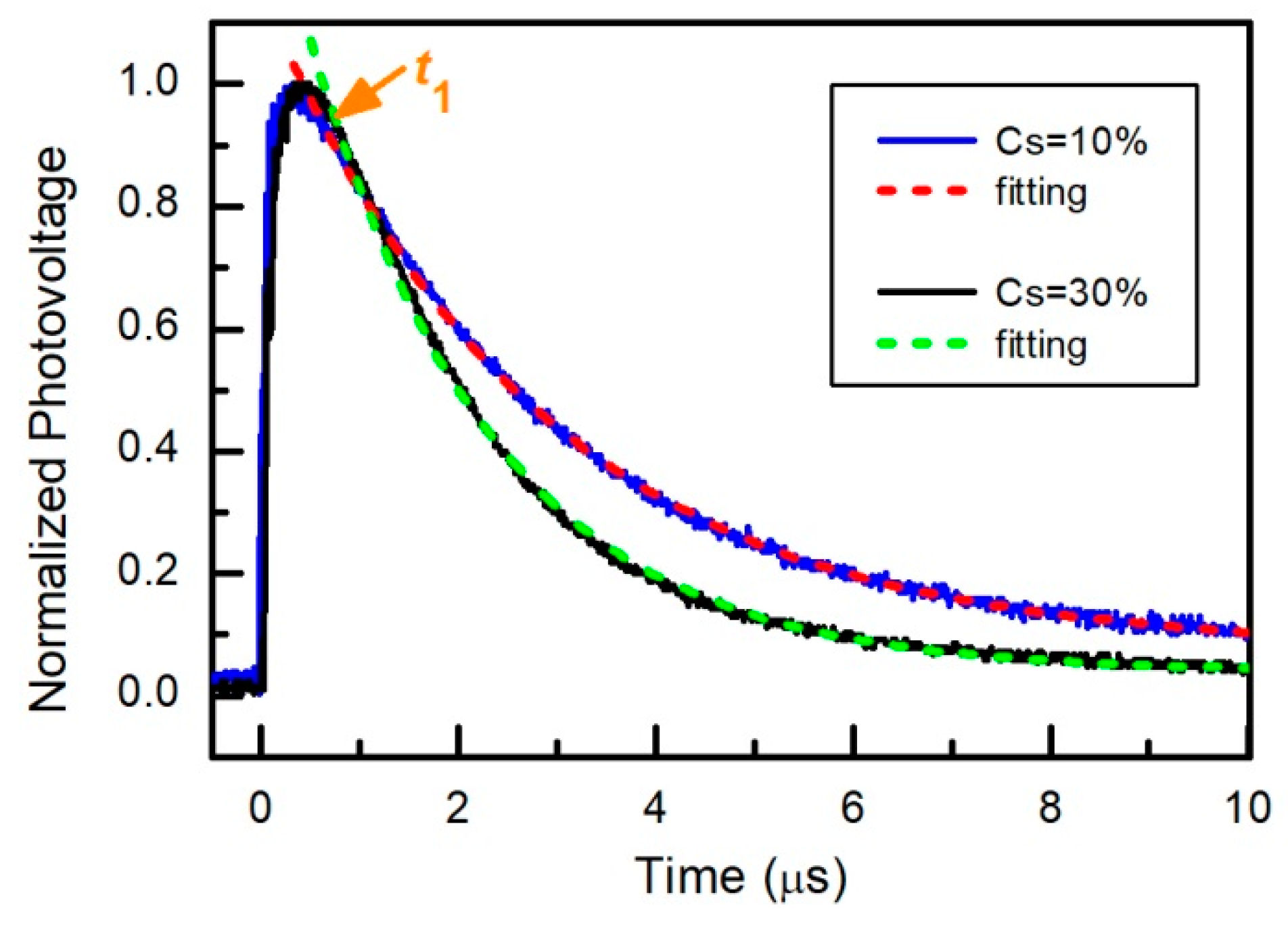
3. Results and Discussion

The grain size and morphology of the perovskite films grown on mesoporous TiO2 scaffolds were strongly dependent on cesium concentration in the precursor solution. The top-view SEM images of the triple cation perovskite films prepared from solution containing different concentration of Cs (0, 10, 20, and 40%) are shown in Figure 2.
It is seen that morphology of the perovskite layer without cesium (0 Cs) can be characterized by formation of big grains of ~400–900 nm in size. It is worth noting that in this case (perovskite without Cs) significantly smaller grains which are attributed to an individual PbI2 phase tend to be formed at the perovskite grains’ boundaries [55]. Addition of CsI to the precursors solution and resulting incorporation of Cs+ ions into the layer structure lead to formation of considerably smaller perovskite grains because Cs-induced perovskite seeds become nucleation sites for further crystal growth and thus lead to more uniform grains [49,55]. When the layers contain 10 and 20% of Cs, the grains of ~100–200 nm in size prevail, and their boundaries are clearly distinct. Futher increase of CsI content in the solution leads to the change in the morphology of the formed perovskite layers: the grains show a tendency to form larger agregates, they seem to be more integral, i.e., their boundaries are not so clearly distinct (Figure 2, 40 Cs). At higher concentration of Cs (more than 20%), not all Cs ions get into the perovskite lattice, and their excess can form a mixed compound with Pb (as a separate phase on the surface of the layer) [77] and/or is flushed out by chlorobenzene in step III of the fabrication. Distribution of Cs on the surface of perovskite layer can be clearly seen in Figure 3 where the EDX mapping is presented.
As Figure 3 shows, the EDX images confirm that Br, Sn, I, and Pb elements are homogeneously dispersed while Cs is segregated into 2–5 m-size islands. The details of the elemental composition of the sample surface at points 1 and 2 are presented in Table 1.
Morphological changes of the same perovskite samples are significantly less pronounced in the cross-sectional SEM images (Figure 4). At higher Cs concentration (20% and 40%), the perovskite layers look amorphous since crystals or crystalline aggregates (conglomerates) are hardly visible (Figure 4c,d). The thickness of the perovskite films grown on meso-TiO2 is in the range of 850 nm to 1100 nm.
Influence of Cs on structure and phase composition of the formed perovskite layers was studied by the XRD technique with Cs concentration ranging from 0 to 60%. Figure 5 shows fragments of the measured XRD patterns.
No Cs containing film demonstrated XRD peaks that could be attributed to MA0.17FA0.83Pb(Br0.17I0.83)3 phase with cubic crystal lattice (a = 6.284 Å) and to PbI2 which are both characteristic of perovskite films without Cs+ ions. Addition of 10% of CsI into the precursor solution resulted in vanished PbI2 phase. However, additional peaks emerged at 2Θ angles of 11.53° and 12.87°. The last peak could be attributed to possible solid solution of PbxCsx−1I2 since the replacement of Pb ions by those of smaller ionic radius Cs should cause a shift of peak towards bigger 2Θ angles. In case of 20% of Cs containing film, rather strong peak at 2Θ angle of 11.6° emerged on the XRD pattern, and the peak of the perovskite phase was shifted to lower diffraction angles. This could be caused by the presence of hexagonal (P63/mmc) polytypes of the perovskite [78]. The low intensity peak at 2Θ angle of 13.06° indicated presence of small amount of CsPbI3 in the film. Bigger quantity of Cs+ ions caused formation of two perovskite phases with cubic structure since each perovskite peak on the XRD pattern split into two peaks. The structure with larger crystal lattice (a = 6.304 Å) showed lower volume percentage while that with smaller lattice (a = 6.241 Å) was bigger in quantity according to higher intensity of the corresponding peaks. Decrease of the perovskite lattice parameter most probably results from the replacement of MA+ ions by those of smaller radius Cs+. Increase of the lattice parameter could be caused by the rise of I/Br or/and FA/MA ratios in the perovskite crystal lattice. On the other hand, the peak at 2Θ angle of 14.0° could be related to the 6H polytype of the perovskite [78]. It means that high Cs concentration leads to structural inhomogeneities, crystal cleavages, and phase segregation, all these being detrimental to device performance and potentially serving as recombination centers [79].
The measured absorbance spectra of the perovskite Csx(MA0.17FA0.83)1−x Pb(I0.83Br0.17)3 films with different cesium concentration are shown in Figure 6.
It is seen that introduction of Cs into the perovskite causes gradual blue-shift of the absorption spectrum. When small amount of Cs (x ≤ 0.1) is introduced, absorbance of the perovskite layer in the visible spectrum range increases, and then begins to decrease at higher cesium concentration (x > 0.1). The observed weakening of the absorption with higher cesium concentration seems to be stipulated by segregation of CsPbI3 phases or 6H polytype of perovskite as mentioned earlier. Decrease of the absorbance of the perovskite layer with higher Cs concentration was previously observed in other works [49,79]. It should be noted that absorption of the infrared spectrum range in 40% of Cs-containing perovskite layer is high enough due to strong scattering of light by structural inhomogeneities, crystal cleavages, and phase segregation [79].
Photoluminescence spectra of the perovskite layers are shown in Figure 7. Increase in Cs concentration shifts PL maximum to the blue side. However, the red shift is detected in the sample with the highest, 60%, concentration. Similar tendencies were observed in references [49,80]. This red-shift could be explained by the presence of the second cubic or hexagonal 6H polytype of perovskite as mentioned above.
Each peak (λmax is the wavelength of the peak maximum) was convoluted by the two-amplitude version of the Gaussian function y ( λ ) = A i e ( λ λ c i ) 2 2 ω i 2 , where λci is the peak center, ωi is the width (full width at half maximum y ( λ ) = A i e ( λ λ c i ) 2 2 ω i 2 , and Ai is the height of the Gaussian peaks. Results of the best convolution are shown in the inset of Figure 7 and Table 2.
Gaussian peaks G1 and G2 could be related to band–band and excitonic transitions in the samples with lower Cs concentration. Meanwhile, in the samples with 20% and 60% of Cs, peak G2 could be related to the transitions of two different phases due to the decreased difference between the peak centers in accordance with the XRD results. A Tauc plot was used to determine the optical band gap. These values and corresponding wavelengths are presented in Table 2. One can observe good correlation between the band gap wavelength and Gaussian peak G1, except the cases of 40 and 60 percent of Cs. The latter discrepancy is also related to the presence of the second cubic or hexagonal 6H polytype of the perovskite. Another possible explanation of the PL spectrum asymmetry could be related to spatial potential fluctuations and to transitions from band to the tail of the localized states. This asymmetric spectrum can be fitted by a double sigmoid function [81]. We used it in the form of asymmetric
y ( λ ) = A 1 1 + e λ λ c + ω / 2 ω 1 ( 1 1 1 + e λ λ c ω / 2 ω 2 ) ,
where A, λc, ω is the maximum amplitude, the center and the width of the curve, respectively; and ω1, ω2 are the shape parameters of short- and long-wavelength side. Fitting results of Equation (1) are presented in Table 2. Changes of the width ω and long-wavelength side shape parameter ω2 correlate with the changes of the average decay times (see Table 2 and Figure 8).
The transient PL curves measured in the peak center were fitted using multi-exponential model
I PL ( t ) = i A i e t τ i ,
where τi and Ai are the decay time constant and the amplitude of the ith component, respectively. However, only at least three exponents provided good fitting, and these results are shown in Figure 9 with corresponding time constant values.
Two of the decay time constants we assign to the transitions related with the Gaussian peaks. The third decay time could be related with various nonradiative processes, or the longest decay time could be attributed to carrier trapping and detrapping processes [82]. Decrease of the decay time constants with higher Cs concentration we relate with increased number of defects and surface recombination. As a rule, low purity samples have lower values of the decay constants [83]. The average decay time constant was calculated as
τ ¯ = i A i τ i 2 i A i τ i
and was compared with the decay time constants obtained from other fittings and from the transient photovoltage measurement (see Figure 8).
Notwithstanding the application of the three decay times, one cannot explain the case of transition from band to localized states’ tail even by taking into account the trapping-detrapping processes. Thus, we fitted the transients with more general decay function encompassing both the stretched exponential and the compressed hyperbola function [84] as
I PL ( t ) = A e 1 ( 1 + α t τ 0 ) β α β ,
where α and β are the dimensionless parameters. Then the average decay time constant was calculated numerically using the following equation:
τ ¯ = 0 t I PL ( t ) d t 0 I PL ( t ) d t .
The fitting results are also presented in Table 2 and Figure 8. The averaged decay time constants obtained by means of Equations (3) and (5) show the same tendency; see, respectively, PL (3) and PL (5) in Figure 8. The only exception is the sample with 20% of Cs whose averaged decay time constant given by Equation (5) goes to infinity. For comparison, we extracted one-exponent decay time constant ranging from 400 ns up to 700 ns (see PL 1 exp in Figure 8).
Figure 10 shows transients of photovoltage measured across the perovskite solar cell with different cesium concentration.
It is seen that, in a certain interval of time (t > t1), the decay of the photovoltage can be approximated as a simple exponential function U ph = U ph 0 e t / τ , where Uph0 is the value of Uph at time t1, and τ is the characteristic decay time constant. The dependence of the transient photovoltage time constant on cesium concentration is depicted in Figure 8. PV and PL decay times increase only after addition of small amount of Cs, and later start decreasing. This dependence can be explained by the change in the layer quality that leads to reduction of the trap density and charge recombination rates in the perovskite layers [57]. Adding of Cs firstly minimizes the quantity of PbI2 phase, but later there appears CsPbI3 and other polytypes of the perovskite (see Figure 5). It is seen that all the photovoltage time constants have values higher than those obtained from the photoluminescence measurements. This difference could be explained by several reasons [85]. First, the real bulk carrier lifetime is masked by the combination of the surface recombination and self-absorption of reemitted photons in the volume of the perovskite layer. Therefore, the PL decay time can be shorter by an order of magnitude than the real bulk lifetime. Second, the photovoltage decay reflects the bulk recombination processes and produces a proper value of the latter. Third, in the case of a thin film, the transient photovoltage decay is strongly extended by the low ambipolar mobility resulting from the space charge-limited currents.
Figure 11 shows current-forward bias voltage characteristics of the fabricated perovskite solar cells with different cesium concentration. As expected, the cell containing 10% of cesium in the perovskite layer has the highest value of the short-current density Jsc. This is the result of the highest absorbance of the 10%-perovskite layer. This sample also demonstrates the highest values of the photovoltage and the PL decay time constants. It is worth noting that the current-voltage characteristics of solar cell containing 10% of Cs shows negligible hysteresis, just like it was observed earlier in References [49,58,75]. Significant hysteresis of the characteristic was observed only in the case of high cesium concentration (≥20%). This behavior might be related to the phase segregation within the cubic perovskite phase and to reduced crystallinity [79,80].
The values of photovoltaic quantities of the best perovskite solar cells are presented in Table 3, and statistics of the power conversion efficiency of 90 perovskite solar cells with different cesium concentration is depicted in Figure 12.
The run of PCE dependence on cesium concentration agrees with those of light absorbance, transient photovoltage, and PL decay time constants (see Figure 6 and Figure 8). Subsequently, it is obvious that performance of the perovskite solar cells is strongly determined by the quality of the perovskite films mainly represented by a long carrier lifetime and strong light absorption.

4. Conclusions

We experimentally investigated surface morphology, photoluminescence, and optoelectronic properties of perovskite Csx(MA0.17FA0.83)1−x Pb(I0.83Br0.17)3 films with different Cs dosage ranging from x = 0 to x = 0.6. Addition of small amount of Cs (x up to 0.1) leads to increased charge carrier lifetime and better performance of the perovskite solar cells (PCE = 20.2% in case of x = 0.1). At higher cesium concentration, x > 0.1, the carrier lifetime decreases and, as a result, PCE of the solar cells also drops down. An X-ray diffraction and SEM morphology studies of the perovskite films reveal that high dosage of Cs (x > 0.2) causes phase segregation which in turn leads to weaker light absorption due to formed CsPbI3 regions. The presented results provide a background for further improvement of material synthesis and device fabrication in the efforts of development of higher performance perovskite solar cells.

Author Contributions

Conceptualization and methodology, S.A. and K.L.; sample fabrication, A.G., K.P. and A.S. (Algirdas Selskis); formal analysis, A.S. (Algirdas Selskis), and A.S. (Algirdas Sužiedėlis); experimental investigation, E.Š., K.P., A.Č., R.J. and A.L.; writing, reviewing and editing, S.A., J.G. and K.L.; visualization, A.S. (Algirdas Selskis) and K.P.; project administration and supervision, S.A. All authors have read and agreed to the published version of the manuscript.

Funding

This research was funded by Research Council of Lithuania, Grant number 01.2.2-LMT-K-718-01-0050.

Institutional Review Board Statement

Not applicable.

Informed Consent Statement

Not applicable.

Data Availability Statement

No new data were created or analyzed in this study. Data sharing is not applicable to this article.

Acknowledgments

We are sincerely thankful to Dr. Skaidra Bumelienė for her good will in preparation of the article manuscript.

Conflicts of Interest

The authors declare no conflict of interest.

References

  1. Kojima, A.; Teshima, K.; Shirai, Y.; Miyasaka, T. Organometal halide perovskites as visible-light sensitizers for photovoltaic cells. J. Am. Chem. Soc. 2009, 131, 6050–6051. [Google Scholar] [CrossRef]
  2. Lee, M.M.; Teuscher, J.; Miyasaka, T.; Murakami, T.N.; Snaith, H.J. Efficient hybrid solar cells based on meso-superstructured organometal halide perovskites. Science 2012, 338, 643–647. [Google Scholar] [CrossRef] [Green Version]
  3. Liu, M.; Johnston, M.B.; Snaith, H.J. Efficient planar heterojunction perovskite solar cells by vapour deposition. Nature 2013, 501, 395–398. [Google Scholar] [CrossRef]
  4. Yang, W.S.; Park, B.W.; Jung, E.H.; Jeon, N.J.; Kim, Y.C.; Lee, D.U.; Shin, S.S.; Seo, J.; Kim, E.K.; Noh, J.H.; et al. Iodide management in formamidinium-lead-halide-based perovskite layers for efficient solar cells. Science 2017, 356, 1376–1379. [Google Scholar] [CrossRef] [Green Version]
  5. Li, T.; Pan, Y.; Wang, Z.; Xia, Y.; Chen, Y.; Huang, W. Additive engineering for highly efficient organic-inorganic halide perovskite solar cells: Recent advances and perspectives. J. Mater. Chem. A 2017, 5, 12602–12652. [Google Scholar] [CrossRef]
  6. Gao, X.-X.; Xue, D.-J.; Gao, D.; Han, Q.; Ge, Q.-Q.; Ma, J.-Y.; Ding, J.; Zhang, W.; Zhang, B.; Feng, Y.; et al. High-mobility hydrophobic conjugated polymer as effective interlayer for air-stable efficient perovskite solar cells. Sol. RRL 2018, 3, 1800232. [Google Scholar] [CrossRef] [Green Version]
  7. Shi, Z.; Jayatissa, A.H. Perovskites-based solar cells: A review of recent progress, materials and processing methods. Materials 2018, 11, 729. [Google Scholar] [CrossRef] [Green Version]
  8. Mesquita, I.; Andrade, L.; Mendes, A. Perovskite solar cells: Materials, configuration and stability. Renew. Sustain. Energy Rev. 2018, 82, 2471–2489. [Google Scholar] [CrossRef]
  9. Laalioui, S.; Alaoui, K.B.; Dads, H.A.; Assali, K.E.; Ikken, B.; Outzourhit, A. Progress in perovskite based solar cells: Scientific and engineering state of the art. Rev. Adv. Mater. Sci. 2020, 59, 10–25. [Google Scholar] [CrossRef]
  10. Liu, F.; Zeng, Q.; Li, J.; Hao, X.; Ho-Baillie, A.; Tang, J.; Green, M.A. Emerging inorganic compound thin film photovoltaic materials: Progress, challenges and strategies. Mater. Today 2020, 41, 120–142. [Google Scholar] [CrossRef]
  11. Jeong, M.; Choi, I.W.; Go, E.M.; Kim, M.; Lee, B.; Jeong, S.; Jo, Y.; Choi, H.W.; Lee, J.; Bae, J.-H.; et al. Stable perovskite solar cells with efficiency exceeding 24.8% and 0.3-V voltage loss. Science 2020, 369, 1615–1620. [Google Scholar] [CrossRef] [PubMed]
  12. Kim, J.Y.; Lee, J.-W.; Jung, H.S.; Shin, H.; Park, N.-G. High efficiency perovskite solar cells. Chem. Rev. 2020, 120, 7867–7918. [Google Scholar] [CrossRef] [PubMed]
  13. Dai, Z.; Yadavalli, S.K.; Chen, M.; Abbaspourtamijani, A.; Qi, Y.; Padture, N.P. Interfacial toughening with self-assembled monolayers enhances perovskite solar cell reliability. Science 2021, 372, 618–622. [Google Scholar] [CrossRef] [PubMed]
  14. Dou, L.; Yang, Y.M.; You, J.; Hong, Z.; Chang, W.-H.; Li, G.; Yang, Y. Solution-processed hybrid perovskite photodetectors with high detectivity. Nat. Commun. 2014, 5, 5404. [Google Scholar] [CrossRef]
  15. Dong, R.; Fang, Y.; Chae, J.; Dai, J.; Xiao, Z.; Dong, Q.; Yuan, Y.; Centrone, A.; Zeng, X.C.; Huang, J. High-gain and low-driving-voltage photodetectors based on organolead triiodide perovskites. Adv. Mater. 2015, 27, 1912–1918. [Google Scholar] [CrossRef]
  16. Dong, Y.; Zou, Y.; Song, J.; Song, X.; Zeng, H. Recent progress of metal halide perovskite photodetectors. J. Mater. Chem. C 2017, 5, 11369–11394. [Google Scholar] [CrossRef]
  17. Feng, J.; Gong, C.; Gao, H.; Wen, W.; Gong, Y.; Jiang, X.; Zhang, B.; Wu, Y.; Wu, Y.; Fu, H.; et al. Single-crystalline layered metal-halide perovskite nanowires for ultrasensitive photodetectors. Nat. Electron. 2018, 1, 404–410. [Google Scholar] [CrossRef]
  18. Wu, H.; Si, H.; Zhang, Z.; Kang, Z.; Wu, P.; Zhou, L.; Zhang, S.; Zhang, Z.; Liao, Q.; Zhang, Y. All-inorganic perovskite quantum dot-monolayer MoS2 ultrasensitive photodetector. Adv. Sci. 2018, 5, 1801219. [Google Scholar] [CrossRef] [Green Version]
  19. Gegevičius, R.; Franckevičius, M.; Pakštas, V.; Augulis, R.; Gulbinas, V. High-speed, sensitive planar perovskite photodetector based on interdigitated Au electrodes. Phys. Status Solidi A 2018, 215, 1700822. [Google Scholar] [CrossRef]
  20. Mei, F.; Sun, D.; Mei, S.; Feng, J.; Zhou, Y.; Xu, J.; Xiao, X. Recent progress perovskite-based photodetectors: The design of materials and structures. Adv. Phys. X 2019, 4, 1592709. [Google Scholar] [CrossRef] [Green Version]
  21. Ma, Z.; Zhang, Y.; Li, T.; Tang, X.; Zhao, H.; Li, J.; Ma, C.; Yao, J. High-performance self-powered perovskite photodetector for visible light communication. Appl. Phys. A 2020, 126, 869. [Google Scholar] [CrossRef]
  22. Zhang, Y.; Lyu, M.; Qiu, T.; Han, E.; Kim, I.K.; Jung, M.-C.; Ng, Y.H.; Yun, J.-H.; Wang, L. Halide perovskite single crystals: Optoelectronic applications and strategical approaches. Energies 2020, 13, 4250. [Google Scholar] [CrossRef]
  23. Wu, D.; Li, W.; Liu, H.; Xiao, X.; Shi, K.; Tang, H.; Shan, C.; Wang, K.; Sun, X.W.; Kyaw, A.K.K. Universal strategy for improving perovskite photodiode performance: Interfacial built-in electric field manipulated by unintentional doping. Adv. Sci. 2021, 202101729. [Google Scholar] [CrossRef]
  24. Tan, Z.-K.; Moghaddam, R.S.; Lai, M.L.; Docampo, P.; Higler, R.; Deschler, F.; Price, M.; Sadhanala, A.; Pazos, L.M.; Credgington, D.; et al. Bright light-emitting diodes on organometal halide perovskite. Nat. Nanotechnol. 2014, 9, 687–692. [Google Scholar] [CrossRef] [PubMed]
  25. Zhao, L.; Yeh, Y.-W.; Tran, N.L.; Wu, F.; Xiao, Z.; Kerner, R.A.; Lin, Y.L.; Scholes, G.D.; Yao, N.; Rand, B.P. In situ preparation of metal halide perovskite nanocrystal thin films for improved light-emitting devices. ACS Nano 2017, 11, 3957–3964. [Google Scholar] [CrossRef] [PubMed]
  26. Mao, J.; Lin, H.; Ye, F.; Qin, M.; Burkhartsmeyer, J.M.; Zhang, H.; Lu, X.; Wong, K.S.; Choy, W.C.H. All-perovskite emission architecture for white light-emitting diodes. ACS Nano 2018, 12, 10486–10492. [Google Scholar] [CrossRef] [PubMed]
  27. Stranks, S.D.; Hoye, R.L.Z.; Di, D.; Friend, R.H.; Deschler, F. The physics of light emission in halide perovskite devices. Adv. Mater. 2018, 1, 1803336. [Google Scholar] [CrossRef] [Green Version]
  28. Kim, Y.-H.; Kim, S.; Jo, S.H.; Lee, T.-W. Metal halide perovskites: From crystal formations to light-emitting-diode applications. Small Methods 2018, 2, 1800093. [Google Scholar] [CrossRef]
  29. Li, Z.; Chen, Z.; Yang, Y.; Xue, Q.; Yip, H.-L.; Cao, Y. Modulation of recombination zone position for quasi-two-dimensional blue perovskite light-emitting-diodes with efficiency exceeding 5%. Nat. Commun. 2019, 10, 1027. [Google Scholar] [CrossRef]
  30. Bao, C.; Muhammad, M.; Ma, X.; Wang, Z.; Liu, Y.; Cnen, P.; Chen, S.; Liu, B.; Wang, J.; Duan, Y. Hybrid perovskite charge generation layer for highly efficient tandem organic light-emitting diodes. Org. Electron. 2019, 73, 299–303. [Google Scholar] [CrossRef]
  31. Chen, S.; Chen, V.; Bao, C.; Mujahid, M.; Li, Y.; Chen, P.; Duan, Y. White light-emitting devices based on inorganic perovskite and organic materials. Molecules 2019, 24, 800. [Google Scholar] [CrossRef] [PubMed] [Green Version]
  32. Zhao, H.; Ding, H.; Li, S.; Liu, M.; Yang, J.; Zhao, Y.; Pan, N.; Wang, X. Improving electron injectionin all-inorganic perovskite light-emitting diode via electron transport layer modulation. Optik 2019, 191, 68–74. [Google Scholar] [CrossRef]
  33. Chen, Z.; Li, Z.; Hopper, T.R.; Bakulin, A.A.; Yip, H.-L. Materials, photophysics and device engineering of perovskite light-emitting-diodes. Rep. Prog. Phys. 2021, 84, 046401. [Google Scholar] [CrossRef] [PubMed]
  34. Chen, J.; Wang, J.; Xu, X.; Li, J.; Song, J.; Lan, S.; Liu, S.; Cai, B.; Han, B.; Precht, J.T.; et al. Efficient and bright light-emitting-diodes based on single-layer heterophase halide perovskite. Nat. Photonics 2021, 15, 238–244. [Google Scholar] [CrossRef]
  35. Zhu, Y.; Liu, Y.; Miller, A.M.; Zhu, H.; Egap, E. Lead halide perovskite nanocrystals as photocatalysts for PET-RAFT polymerization under visible and near-infrared irradiation. ACS Macro Lett. 2020, 9, 725–730. [Google Scholar] [CrossRef]
  36. Kar, M.R.; Chakraborty, R.; Patel, U.; Chakraborty, R.; Ray, S.; Acharija, T.K.; Coswami, C.; Bhaumik, S. Impact of Zn-doping on composition, stability, luminescence properties of silica coated all-inorganic cesium lead bromide nanocrystals and their biocompatibility. Mater. Today Chem. 2022, 23, 100753. [Google Scholar] [CrossRef]
  37. De Wolf, S.; Holovsky, J.; Moon, S.-J.; Löper, P.; Niesen, B.; Ledinsky, M.; Haug, F.-J.; Yum, J.-H.; Ballif, C. Organometallic halide perovskites: Sharp optical absorption edge and its relation to photovoltaic performance. J. Phys. Chem. Lett. 2014, 5, 1035–1039. [Google Scholar] [CrossRef]
  38. Quan, L.N.; Rand, B.P.; Friend, R.H.; Mhaisalkar, S.G.; Lee, T.W.; Sargent, E.H. Perovskites for next-generation optical sources. Chem. Rev. 2019, 119, 7444–7478. [Google Scholar] [CrossRef]
  39. Kothandaraman, R.K.; Jiang, Y.; Feurer, T.; Tiwari, A.N.; Fu, F. Near-infrared-transparent perovskite solar cells and perovskite-based tandem photovoltaics. Small Methods 2020, 4, 2000395. [Google Scholar] [CrossRef]
  40. Wehrenfennig, C.; Eperon, G.E.; Johnston, M.B.; Snaith, H.J.; Herz, L.M. High carrier mobilities and lifetimes in organolead trihalide perovskites. Adv. Mater. 2014, 26, 1584–11589. [Google Scholar] [CrossRef] [Green Version]
  41. Karakus, M.; Jensen, S.A.; D’Angelo, F.; Turchinovich, D.; Bonn, M.; Cánovas, E. Phonon-electron scattering limits free charge mobility in methylammonium lead iodide perovskites. J. Phys. Chem. Lett. 2015, 6, 4991–4996. [Google Scholar] [CrossRef] [PubMed]
  42. Stranks, S.D.; Eperon, G.E.; Grancini, G.; Menelaou, C.; Alcicer, M.J.P.; Leijens, T.; Herz, L.M.; Petrozza, A.; Snaith, H.J. Electron-hole diffusion lengths exceeding 1 micrometer in an Organometal trihalide perovskite absorber. Science 2013, 342, 341–344. [Google Scholar] [CrossRef] [PubMed] [Green Version]
  43. Dong, Q.; Fang, Y.; Shao, Y.; Mulligan, P.; Cao, L.; Huang, J. Electron-hole diffusion lengths >175 µm in solution-grown CH3NH3PbI3 single crystals. Sci. Express 2015, 6225. [Google Scholar] [CrossRef] [Green Version]
  44. Jeon, N.J.; Noh, J.H.; Yang, W.S.; Kim, Y.C.; Ryu, S.; Seo, J.; Seok, S.I. Compositional engineering of perovskite materials for high-performance solar cells. Nature 2015, 517, 476–480. [Google Scholar] [CrossRef] [PubMed]
  45. Eperon, G.; Hörantner, M.T.; Snaith, H.J. Metal halide perovskite tandem and multiple-junction photovoltaics. Nat. Rev. Chem. 2017, 1, 0095. [Google Scholar] [CrossRef]
  46. Unger, E.L.; Kegelman, L.; Suchan, K.; Sörell, D.; Korte, L.; Albrecht, S. Roadmap and roadblocks for the band gap tunability of metal halide perovskites. J. Mater. Chem. A 2017, 5, 11401–11409. [Google Scholar] [CrossRef]
  47. Wang, L.; Shahiduzzaman, M.; Muslih, Y.M.; Nakano, M.; Karakawa, M.; Takahachi, K.; Tomita, K.; Ninzi, J.M.; Taima, T. Double-layer CsI intercalation into MAPbI3 framework for efficient and stable perovskite solar cells. Nano Energy 2021, 86, 106135. [Google Scholar] [CrossRef]
  48. Correa-Baena, J.P.; Steier, L.; Tress, W.; Saliba, M.; Neutzner, S.; Matsui, T.; Giordano, F.; Jacobsson, T.J.; Kandada, A.R.S.; Zakeeruddin, S.M.; et al. Highly efficient planar perovskite solar cells through band alignment engineering. Energy Environ. Sci. 2015, 8, 2928–2934. [Google Scholar] [CrossRef] [Green Version]
  49. Saliba, M.; Matsui, T.; Seo, J.Y.; Domaski, K.; Correa-Baena, J.P.; Nazeeruddin, M.K.; Zakeeruddin, S.M.; Tress, W.; Abate, A.; Hagfeldt, A.; et al. Cesium-containing triple cation perovskite solar cells: Improved stability, reproducibility and high efficiency. Energy Environ. Sci. 2016, 9, 1989–1997. [Google Scholar] [CrossRef] [Green Version]
  50. Correa-Baena, J.P.; Saliba, M.; Buonassisi, T.; Grätzel, M.; Abate, A.; Tress, W.; Hagfeldt, A. Promises and challenges of perovskite solar cells. Science 2017, 358, 739–744. [Google Scholar] [CrossRef] [Green Version]
  51. Christians, J.A.; Schulz, P.; Tinkham, J.; Schloemer, T.H.; Harvey, S.P.; Tremolet de Villers, B.J.; Sellinger, A.; Berry, J.J.; Luther, J.M. Taylored interfaces of unencapsulated perovskite solar cells for >1000 hour operational stability. Nat. Energy 2018, 3, 68–74. [Google Scholar] [CrossRef]
  52. Shen, H.; Omelchenko, S.T.; Jacobs, D.A.; Yalamanchili, S.; Wan, Y.; Yan, D.; Phang, P.; Duong, T.; Wu, Y.; Yin, Y.; et al. In situ recombination junction between p-Si and TiO2 enables high-efficiency monolithic perovskite/Si tandem cells. Sci. Adv. 2018, 4, eaau9711. [Google Scholar] [CrossRef] [PubMed] [Green Version]
  53. Mateen, M.; Arain, Z.; Liu, X.; Liu, C.; Yang, Y.; Ding, Y.; Ma, S.; Ren, Y.; Wu, Y.; Tao, Y.; et al. High-performance mixed-cation mixed–halide perovskite solar cells enabled by a facile intermediate engineering technique. J. Power Sources 2020, 448, 227386. [Google Scholar] [CrossRef]
  54. Liu, P.; Liu, Z.; Qin, C.; He, T.; Li, B.; Ma, L.; Shaheen, K.; Yang, K.; Yang, H.; Liu, H.; et al. High-performance perovskite solar cells based on passivating interfacial and intergranular defects. Sol. Energy Mater. Sol. Cells 2020, 212, 110555. [Google Scholar] [CrossRef]
  55. Cho, H.; Kim, J.S.; Wolf, C.; Kim, Y.-H.; Yun, H.J.; Jeong, S.-H.; Sadhanala, A.; Venugopalan, V.; Choi, J.W.; Lee, C.-L.; et al. High-efficiency plycrystalline perovskite light-emitting diodes based on mixed cations. ACS Nano 2018, 12, 2883–2892. [Google Scholar] [CrossRef]
  56. Jena, A.K.; Kulkarni, A.; Miyasaka, T. Halide perovskite photovoltaic: Background, status, and future prospects. Chem. Rev. 2019, 119, 3036–3103. [Google Scholar] [CrossRef]
  57. Hu, Y.; Hutter, E.M.; Rieder, P.; Grill, I.; Hanisch, J.; Aygüler, M.F.; Hufnagel, A.G.; Handloser, M.; Bein, T.; Hartschun, A.; et al. Understanding the role of cesium and rubidium additives in perovskite solar cells: Trap states, charge transport, and recombination. Adv. Energy Mater. 2018, 1703057. [Google Scholar] [CrossRef]
  58. Ašmontas, S.; Čerškus, A.; Gradauskas, J.; Grigucevičienė, A.; Leinartas, K.; Lučun, A.; Petrauskas, K.; Selskis, A.; Sužiedelis, A.; Širmulis, E.; et al. Cesium-containing triple cation perovskite solar cells. Coatings 2021, 11, 279. [Google Scholar] [CrossRef]
  59. Lee, J.W.; Kim, D.H.; Kim, H.S.; Seo, S.W.; Cho, S.M.; Park, N.G. Formamidinium and cesium hybridization for photo- and moisture-stable perovskite solar cell. Adv. Energy Mater. 2015, 5, 1501310. [Google Scholar] [CrossRef]
  60. Liu, T.; Zong, Y.; Zhou, Y.; Yang, M.; Li, Z.; Game, O.S.; Zhu, K.; Gong, Q.; Padture, N.P. High-performance formamidinium–based perovskite solar cells via microstructure-mediated δ–to–α phase transformation. Chem. Mater. 2017, 29, 3246–3250. [Google Scholar] [CrossRef]
  61. Rehman, W.; McMeekin, D.P.; Patel, J.B.; Milot, R.L.; Johnston, M.B.; Snaith, H.J.; Herz, L.M. Photovoltaic mixed-cation lead mixed-halide perovskite: Links between crystallinity, photo-stability and electronic properties. Energy Environ. Sci. 2017, 10, 361–369. [Google Scholar] [CrossRef] [Green Version]
  62. Herz, L.M. Charge-carrier mobilities in metal halide perovskites: Fundamentals mechanisms and limits. ACS Energy Lett. 2017, 2, 1539–1548. [Google Scholar] [CrossRef]
  63. McMeekin, D.P.; Sadoudhi, G.; Rehman, W.; Eperon, G.E.; Saliba, M.; Hörantner, M.T.; Haghighirad, A.; Sakai, N.; Korte, L.; Rech, B.; et al. A mixed-cation lead mixed-halide perovskite absorber for perovskite solar cells. Science 2016, 351, 151–155. [Google Scholar] [CrossRef] [PubMed] [Green Version]
  64. Werner, J.; Niesen, B.; Ballif, C. Perovskite/silicon tandem solar cells: Marriage of convenience or true love story? An overview. Adv. Mater. Interfaces 2018, 5, 1700731. [Google Scholar] [CrossRef]
  65. Zheng, J.; Lau, C.F.J.; Mehrvarz, H.; Ma, F.J.; Jiang, Y.; Deng, X.; Soeriyadi, A.; Kim, J.; Zhang, M.; Hu, L.; et al. Large area efficient interface layer free monolithic perovskite/homo-junction-silicon tandem solar cell with over 20% efficiency. Energy Environ. Sci. 2018, 11, 2432–2443. [Google Scholar] [CrossRef] [Green Version]
  66. Jaysankar, M.; Filipič, M.; Zielinski, B.; Schmager, R.; Song, W.; Qiu, W.; Paetzold, U.W.; Aernouts, T.; Debucquoy, M.; Gehlhaar, R.; et al. Perovskite–silicon tandem solar modules with optimized light harvesting. Energy Environ. Sci. 2018, 11, 1489–1498. [Google Scholar] [CrossRef]
  67. Köhnen, E.; Jošt, M.; Morales-vilches, A.B.; Tockhorn, P.; Al-Ashouri, A.; Macco, B.; Kogelmann, L.; Korte, L.; Rech, B.; Schlatmann, R.; et al. Highly efficient monolithic perovskite silicon solar cells: Analyzing the influence of current mismatch on device performance. Sustain. Energy Fuels 2019, 3, 1995–2005. [Google Scholar] [CrossRef] [Green Version]
  68. Chen, B.; Yu, Z.; Liu, K.; Zheng, X.; Liu, Y.; Shi, J.; Spronk, D.; Rudd, P.N.; Holman, Z.; Huang, J. Grain engineering for perovskite/silicon monolithic tandem solar cells with efficiency of 25.4%. Joule 2019, 3, 177–190. [Google Scholar] [CrossRef] [Green Version]
  69. Shen, H.; Walter, D.; Wu, Y.; Fong, K.C.; Jacobs, D.A.; Duong, T.; Peng, J.; Weber, K.; White, T.P.; Catchpole, K.R. Monolithic perovskite/Si solar cells: Pathways to over 30% efficiency. Adv. Energy Mater. 2019, 10, 1902840. [Google Scholar] [CrossRef]
  70. Duong, T.; Pham, H.; Kho, T.C.; Phang, P.; Fong, K.C.; Yan, D.; Yin, Y.; Peng, J.; Mahmud, M.A.; Charibzadeh, S.; et al. Highly efficiency perovskite-silicon tandem solar cells: Effect of surface coating versus bulk incorporation of 2D perovskite. Adv. Energy Mater. 2020, 10, 1903553. [Google Scholar] [CrossRef]
  71. Al-Ashouri, A.; Köhnen, E.; Li, B.; Magomedov, A.; Hempel, H.; Caprioglio, P.; Márquez, J.A.; Vilches, A.B.; Kasparavičius, E.; Smith, J.A.; et al. Monolithic perovskite/silicon tandem solar cell with >29% efficiency by enhanced hole extraction. Science 2020, 370, 1300–1309. [Google Scholar] [CrossRef] [PubMed]
  72. Yeom, K.M.; Kim, S.U.; Woo, M.Y.; Noh, J.H.; Im, S.H. Recent progress in metal halide perovskite-based tandem solar cell. Adv. Mater. 2020, 32, 2002228. [Google Scholar] [CrossRef] [PubMed]
  73. Yang, D.; Zhang, X.; Hou, Y.; Wang, K.; Ye, T.; Yoon, J.; Wu, C.; Sanghadasa, M.; Liu, S.; Priya, S. 28.3%-efficiency perovskite/silicon tandem solar cell by optimal transparent electrode for high efficient semitransparent top cell. Nano Energy 2021, 84, 105934. [Google Scholar] [CrossRef]
  74. Wu, T.; Qin, Z.; Wang, Y.; Wu, Y.; Chen, W.; Zhang, S.; Cai, M.; Dai, S.; Zhang, J.; Liu, J.; et al. The main progress of perovskitesolar cells in 2020–2021. Nano-Micro Lett. 2021, 13, 152. [Google Scholar] [CrossRef]
  75. Singh, T.; Miyasaka, T. Stabilizing the efficiency beyond 20% with a mixed cation perovskite solar cell fabricated in ambient air under controlled humidity. Adv. Energy Mater. 2018, 8, 1700677. [Google Scholar] [CrossRef]
  76. Domanski, K.; Alharbi, E.A.; Hagfeldt, A.; Grätzel, M.; Tress, W. Systematic investigation of the impact of operation conditions on the degradation behavior of perovskite solar cells. Nat. Energy 2018, 3, 61–67. [Google Scholar] [CrossRef]
  77. Shahiduzzaman, M.; Yonezawa, K.; Yamamoto, K.; Ripolles, T.S.; Karakawa, M.; Kuwabara, T.; Takahashi, K.; Hayase, S.; Taima, T. Improved reproducibility and intercalation control of efficient planar inorganic perovskite solar cells by simple alternate vacuum deposition of PbI2 and CsI. ACS Omega 2017, 11, 4464–4469. [Google Scholar] [CrossRef] [Green Version]
  78. Gratia, P.; Zimmerman, I.; Schouwink, P.; Yum, J.-H.; Audinot, J.-N.; Sivula, K.; Wirtz, T.; Nazeeruddin, M.K. The many faces of mixed ion perovskite: Unraveling and understanding the crystallization process. ACS Energy Lett. 2017, 2, 2686–2693. [Google Scholar] [CrossRef]
  79. Sutanto, A.A.; Queloz, V.I.E.; Garcia-Benito, I.; Smit, B.; Nazeeruddin, M.K.; Syzgantseva, O.A.; Grancini, G. Pushing the limit of Cs incorporation into FAPbBr3 perovskite to enhance solar cell perfomances. APL Mater. 2019, 7, 041110–041111. [Google Scholar] [CrossRef] [Green Version]
  80. Paek, S.; Khan, S.B.; Franckevičius, M.; Gegevičius, R.; Syzgantseva, O.A.; Syzgantseva, M.A.; Kinge, S.; Asiri, A.M.; Roldán-Carmona, C.; Nazeeruddin, M.K. Cation optimization for burn-in loss-free perovskite solar devices. J. Mater. Chem. A 2021, 9, 5374–5380. [Google Scholar] [CrossRef]
  81. Krustok, J.; Collan, H.; Yakushev, M.; Hjelt, K. The role of spatial potential fluctuations in the shape of the PL bands of multinary semiconductor compounds. Phys. Scr. 1999, T79, 179–182. [Google Scholar] [CrossRef]
  82. Chirvony, V.S.; Martínez-Pastor, J.P. Trap-Limited Dynamics of Excited Carriers and Interpretation of the Photoluminescence Decay Kinetics in Metal Halide Perovskites. J. Phys. Chem. Lett. 2018, 9, 4955–4962. [Google Scholar] [CrossRef] [PubMed]
  83. Campbella, S.; Qua, Y.; Majorb, J.D.; Lagardec, D.; Labbéd, C.; Maielloa, P.; Barrioza, V.; Beattiea, N.S.; Zoppi, G.J. Direct evidence of causality between chemical purity and band-edge potential fluctuations in nanoparticle ink-based Cu2ZnSn(S,Se)4 solar cells. Phys. D Appl. Phys. 2019, 52, 135102. [Google Scholar] [CrossRef]
  84. Berberan-Santos, N.M. A luminescence decay function encompassing the stretched exponential and the compressed hyperbola. Chem. Phys. Lett. 2008, 460, 146–150. [Google Scholar] [CrossRef] [Green Version]
  85. Ahrenkiel, R.K.; Johnston, S.W.; Kuciauskas, D.; Tynan, J. Dual-sensor technique for characterization of carrier lifetime decay transients in semiconductors. J. Appl. Phys. 2014, 116, 214510. [Google Scholar] [CrossRef]
Figure 1. Schematic step-like representation of the perovskite solar cell formation.
Materials 15 01936 g001
Figure 2. Surface SEM images of the formed perovskite films. Cs concentration (in %) is: (a) 0, (b) 10, (c) 20, (d) 40. Magnification is 100,000×.
Materials 15 01936 g002
Figure 3. Surface SEM image (a) and mapping images of EDX analysis of 30% CsI containing perovskite layer corresponding to bromine (b), tin (c), iodine (d), cesium (e), and lead (f) mapping.
Materials 15 01936 g003
Figure 4. Cross-sectional SEM images of the fractures of the perovskite cells. Cs concentration (in %) is: (a) 0, (b) 10, (c) 20, (d) 40. Magnification is 65,000×.
Materials 15 01936 g004
Figure 5. Fragments of XRD patterns of perovskite films formed with different concentration of Cs in the precursor solution.
Materials 15 01936 g005
Figure 6. Absorbance spectra of perovskite films with different Cs concentration.
Materials 15 01936 g006
Figure 7. PL spectra of perovskite layers with different cesium concentration. The inset shows position of the PL peak maximum and two Gaussian peaks versus Cs concentration.
Materials 15 01936 g007
Figure 8. Dependence of photovoltage (PV) and photoluminescence (PL) decay time constant on cesium concentration in the perovskite layer.
Materials 15 01936 g008
Figure 9. PL decay transients of the perovskite layers with different cesium concentration. Dotted lines are fittings using Equation (2) with i = 3.
Materials 15 01936 g009
Figure 10. Photovoltage decay transients of the solar cells with different concentrations of Cs in perovskite layer. Excitation laser power density is 1.4 mW/cm2.
Materials 15 01936 g010
Figure 11. Current voltage characteristics of perovskite solar cells with different cesium concentration. Light intensity is 100 mW/cm2 of AM 1.5 spectral lamp.
Materials 15 01936 g011
Figure 12. Statistical distribution of power conversion efficiency of perovskite solar cells versus Cs concentration. Error bars indicate plus or minus one standard deviation from the mean.
Materials 15 01936 g012
Table 1. Elemental composition of the 30% CsI containing perovskite film surface, atomic % (oxygen and titanium values not included).
Point in Figure 3BrSnICsPb
110.74.157.60.822.1
26.32.052.417.517.4
Table 2. Results of PL analysis.
Cs Concentration, %
010204060
Band gap, eV (wavelength, nm)1.61 (770)1.62 (765)1.64 (756)1.63 (760)1.62 (765)
λmax, nm770762752746747
Gaussianλc1, nm767761752739743
ω1 (FWHM), nm11 (26)12 (28)14 (33)37 (87)32 (75)
A1, arb. u.0.290.340.470.130.17
λc2, nm775770756746747
ω2 (FWHM), nm23 (54)25 (59)23 (54)18 (42)17 (40)
A2, arb. u.0.730.690.530.880.83
Equation (1)A, arb. u.2.12.42.31.51.8
λc, nm769761752745747
ω, nm1913153125
ω1, nm1011101012
ω2, nm1517131111
Equations (4) and (5)A, arb. u.0.950.830.790.720.79
α9.5591.31.71.2
β0.370.357E-80.240.19
τ 0 , ns7.60.542.74.76.4
τ ¯ 6982206Inf.108117
Table 3. Photovoltaic parameters of the perovskite solar cells with different cesium concentration.
Cs, %Voc, VJsc, mA·cm−2FF, %PCE, %
01.1320.26414.6
101.1123.67720.2
201.0920.87416.8
401.0118.37113.1
600.9616.07010.8
Publisher’s Note: MDPI stays neutral with regard to jurisdictional claims in published maps and institutional affiliations.

