Abstract
One of the major obstacles in the way of high−performance quantum dot light−emitting diodes (QLEDs) is the charge imbalance arising from more efficient electron injection into the emission layer than the hole injection. In previous studies, a balanced charge injection was often achieved by lowering the electron injection efficiency; however, high performance next−generation QLEDs require the hole injection efficiency to be enhanced to the level of electron injection efficiency. Here, we introduce a solution−processed HfOx layer for the enhanced hole injection efficiency. A large amount of oxygen vacancies in the HfOx films creates gap states that lower the hole injection barrier between the anode and the emission layer, resulting in enhanced light−emitting characteristics. The insertion of the HfOx layer increased the luminance of the device to 166,600 cd/m2, and the current efficiency and external quantum efficiency to 16.6 cd/A and 3.68%, respectively, compared with the values of 63,673 cd/m2, 7.37 cd/A, and 1.64% for the device without HfOx layer. The enhanced light−emitting characteristics of the device were elucidated by X−ray photoelectron, ultra−violet photoelectron, and UV−visible spectroscopy. Our results suggest that the insertion of the HfOx layer is a useful method for improving the light−emitting properties of QLEDs.
1. Introduction
Light−emitting diodes (LEDs) have been extensively researched in the past few decades as a component of electronic devices that have become indispensable for convenient human life. Various types of light−emitting materials, such as organics, perovskites, two−dimensional (2D) materials, and quantum dots (QDs) have been used to produce high brightness LEDs [1,2,3,4]. Among these light−emitting materials, QDs have been extensively emerging owing to their high color purity, solution processability, and facile tunable band gap [5,6].
Unfortunately, the brightness and efficiency of quantum dot light−emitting diodes (QLEDs) are not yet optimal and attempts were made to address these shortcomings by adjusting the charge imbalance between electron and hole injection [7,8,9]. The charge imbalance in QLEDs mainly originates from the presence of excess electrons and numerous studies have been conducted to resolve the problem. Recently, Jin et al. reported the inclusion of an organic electron−blocking layer (EBL) to rectify the charge balance by blocking the injection of electrons [10]. Zhang et al. reported the incorporation of a double−layered structure for electron transport to balance the charge injection [11].
Rather than restricting electron injection to balance the charge injection, another approach would be to improve the hole injection properties for high performance QLED devices. Accordingly, many efforts have been devoted to improve the hole injection characteristics of QLEDs, such as doping the hole injection layer (HIL) or hole transport layer (HTL). However, considering that the hole transporting characteristics are sensitively affected by the amount of dopant material, attaining efficient hole transporting characteristics with an undoped hole injection/transport layer continues to remain a challenge [12]. Attempts to subject the HIL or HTL to additional treatment have also been reported to improve the hole injection properties; however, this simultaneously complicated the device fabrication [13,14]. Therefore, introducing an additional anode buffer layer without doping or post−chemical treatment is necessary for obtaining solution−processed high performance QLEDs.
Here, we introduced a solution−processed HfOx layer as an anode buffer layer to improve the performance of QLEDs. Although the HfOx layer has been widely used as an insulating layer, modification thereof by introducing a large amount of defect states originating from the oxygen vacancies in the HfOx film was expected to lower the hole injection barrier between the anode and emission layer. A large amount of oxygen vacancies was obtained via spin coating followed by thermally annealing the films at low temperature of 250 °C. The maximum luminance, external quantum efficiency, and current efficiency of the optimal device was 166,670 cd/m2, 3.68%, and 16.6 cd/A, respectively. These quantities, which are representative of the QLEDs performance, are more than two−fold higher than those of the device without the HfOx layer, indicating that the HfOx layer efficiently enhanced the performance of the QLEDs.
2. Experimental Section
2.1. Solutions Preparation
Solutions of HfOx with different concentrations were prepared by dissolving different amounts of HfCl4 (Sigma Aldrich, St. Louis, MO, USA) in 10 mL 2−methoxyethanol (Sigma Aldrich) to obtain 0.01, 0.03, and 0.05 M solution, after which the mixture was stirred for 30 min. A solution of vanadium oxide (V2O5) was prepared by dissolving 0.1 mL of vanadium triisopropoxide oxide (Alfa Aesar, Massachusetts, USA) in 13 mL of isopropanol (IPA) in a nitrogen−filled glove box. After vigorously stirring the solution for 30 min, 66.5 μL of deionized (DI) water was dropped into the solution to facilitate hydrolysis. A 1 wt% of Poly[(9,9−dioctylfluorenyl−2,7−diyl)−co−(4,4′−(4−sec−butylphenyl)diphenylamine)] (TFB) solution was prepared by dissolving TFB into p−xylene, followed by stirring at 80 °C for 30 min.
2.2. Device Fabrication
Patterned ITO glass was ultrasonicated with DI water, acetone, and IPA for 10 min. The substrates were dried in a stream of N2 gas, followed by exposure to UV−ozone for 15 min to render the surface hydrophilic and remove residual organics. Subsequently, the HfOx solution was spin−coated onto the substrate at 3000 rpm for 30 s. The spin−coated HfOx films were pre−annealed at 120 °C for 5 min to evaporate the solvents, and finally annealed at 250 °C for 45 min. After the coated substrate was allowed to cool, a V2O5 solution was spin−coated onto the HfOx layer at 3000 rpm for 30 s, followed by annealing at 60 °C for 5 min. Next, a solution of TFB, the HTL material, was spin−coated onto the V2O5 layer at 3000 rpm for 30 s, followed by annealing at 180 °C for 30 min. Then, a solution of CdSe/ZnS QDs (Uniam, 20 mg/mL) was spin−coated onto the TFB layer at 2000 rpm for 30 s, followed by annealing at 100 °C for 10 min. The layer of QDs was covered with a layer of ZnO by spin coating a solution thereof (Avantama, N−10) onto the QDs at 2000 rpm for 30 s, followed by annealing at 100 °C for 10 min. Finally, an aluminum (Al) cathode (thickness: 130 nm) was thermally evaporated under vacuum (~8 × 10⁻⁶ Torr) at a rate of 3 A/s using a metal shadow mask with an illuminating area of 4 mm2.
2.3. Characterization
The electroluminescence characteristics of the QLEDs were measured using an OLED I−V−L test system (M6100, McScience Inc.,Suwon, Republic of Korea), which was equipped with a Keithley 2400 source meter and a Konica Minolta CS−2000 spectroradiometer. The ultra−violet photoelectron spectroscopy (UPS) measurements were performed at the Multidimensional Materials Research Center of Kyung Hee University using a helium discharge lamp (VG Scientific, photon energy 21.22 eV) in a custom−built ultra−high vacuum chamber (base pressure: 5 × 10⁻¹⁰ Torr). A sample bias of −10 V was applied to determine the secondary electron cut−off (SECO) positions when the work function (WF) was measured. All spectra were recorded at room temperature by using a hemispherical analyzer (Scienta SES100, Uppsala, Sweden). The overall energy resolution was approximately 0.1 eV. X−ray photoelectron spectroscopy (XPS) measurements were conducted in an ultrahigh vacuum chamber (~1 × 10⁻⁹ Torr), using a spectrometer (Nexsa, Thermo Fisher Scientific, Massachusetts, USA) with an Al−Kα (1486.6 eV) source. UV−visible measurements were conducted using a UV−vis spectrophotometer (Cary 100, Agilent, Santa Clara, USA) to acquire transmittance spectra of the layers. The surface morphology was investigated using AFM measurement (Dimension 3100 SPM, Bruker, Massachusetts, USA ).
3. Results and Discussion
Figure 1a shows the schematic illustration of the device fabrication. The final structure of the device was ITO/(HfOx)/V2O5/TFB/QDs/ZnO/Al. Figure 1b shows the thickness of HfOx (0.03 M) film obtained from AFM measurement. The thickness was obtained to be 3.7 nm. The thickness of V2O5, TFB, QDs, and ZnO can be estimated to be 4.5, 12, 131, and 38 nm from our previous report [15]. Figure 1c–g shows the surface morphology and 3D topography of HfOx (0.03 M), V2O5, TFB, QD, and ZnO layers, respectively. The root mean square values of the layers were 0.1, 0.24, 0.31, 2.94, and 1.38 nm, respectively.
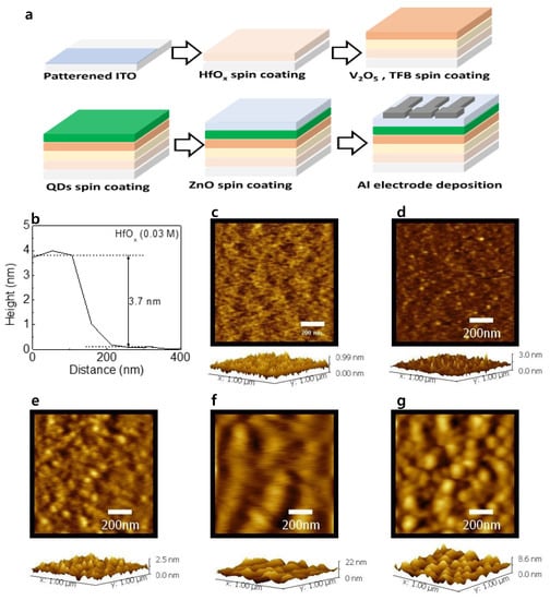
Figure 1.
(a) Schematic illustration of the device fabrication. (b) Thickness of the HfOx (0.03 M) films obtained from AFM measurement. Surface morphology with 3D topography of (c) HfOx (0.03 M), (d) V2O5, (e)TFB, (f) QD, and (g) ZnO layers.
The UPS measurements were intended to determine the WF and valence band maximum (VBM) values of each of the layers from the SECO position and valence region. The SECO and valence region spectra of the ITO, ITO/HfOx (0.01 M), ITO/HfOx (0.03 M), and ITO/HfOx (0.05 M) films are shown in Figure 2a. The obtained WF values of ITO, and ITO/HfOx (0.01, 0.03, and 0.05 M) were 4.02, 4.07, 4.02, and 3.87 eV. The VBM values of HfOx (0.01, 0.03, and 0.05 M) were found to be 3.40, 3.41, and 3.39 eV, respectively. The SECO and valence region spectra of V2O5, HfOx (0.01 M)/V2O5, HfOx (0.03 M)/V2O5, and HfOx (0.05 M)/V2O5 are shown in Figure 2b. The inset shows the near valence region spectra of each of the V2O5 layers, indicating the gap states originating from the V4+ state of V2O5, as previously reported [16,17,18]. The WF values of V2O5 and those of the HfOx (0.01, 0.03, and 0.05 M)/V2O5 layers were 4.94, 5.16, 5.24, and 5.17 eV, respectively. The VBM values of the V2O5 layers were 2.55, 2.55, 2.52, and 2.53 eV, respectively, and the differences between the Fermi level (EF) and gap state were 0.63, 0.61, 0.59, and 0.62 eV, respectively. Figure 2c shows the optical band gaps of the HfOx films in the form of the Tauc plots derived from the UV−vis transmittance, using the following equation
where α is the absorption coefficient, hν is the photon energy, A is a constant, Eg is the optical band gap, and n = 1/2 for a direct band gap semiconductor [19]. All the HfOx films had an optical band gap of 4.86 eV, regardless of the concentration of the HfOx solution. Figure 2d shows the optical band gaps of the V2O5, TFB, and QD layers of 2.67, 2.93, and 2.23 eV, respectively, derived from the Tauc plot. The optical transmission spectra, recorded by conducting UV−vis measurements of the V2O5/TFB/QDs/ZnO films with and without the HfOx layer, are shown in Figure 2e. All the films had high transmittance of more than 90% in the 520–580 nm region regardless of the presence of the HfOx layer, indicating that the HfOx films did not severely affect the transmittance of the device.
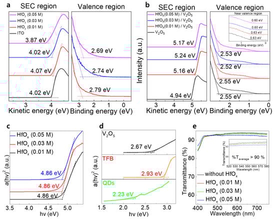
Figure 2.
SEC and valence region spectra of (a) ITO, HfOx (0.01 M), HfOx (0.03 M), and HfOx (0.05 M) films; and (b) V2O5, HfOx (0.01 M)/V2O5, HfOx (0.03 M)/V2O5, and HfOx (0.05 M)/V2O5 films. The inset shows the near valence region spectra of each of the films. Tauc plots of the (c) HfOx (0.01 M), HfOx (0.03 M), and HfOx (0.05 M) films; and (d) V2O5, TFB, and QDs. (e) Optical transmittance spectra of glass/V2O5/TFB/QDs/ZnO films with and without the HfOx layer.
The chemical states of each of the layers in the device were examined in detail by using XPS to analyze for hafnium 4d (Hf 4d) and vanadium 2p (V 2p). Reliability was ensured by calibrating the binding energies by assigning the peak at 285 eV to C 1s. Figure 3a shows the Hf 4d spectra of the HfOx (0.01 M), HfOx (0.03 M), and HfOx (0.05 M) films. The doublet at binding energies of ~224.2 eV and 213.4 eV arose as a result of spin orbit splitting of the Hf 4d orbitals into Hf 4d3/2 and Hf 4d5/2, respectively [20]. Figure 3b–d shows the Hf 4d3/2 XPS results for the HfOx (0.01 M), HfOx (0.03 M), and HfOx (0.05 M) films, respectively. Because all the Hf 4d3/2 peaks were slightly asymmetric, as shown in Figure 3b−d, Hf ions of different valences were considered to exist in the HfOx film. The XPS profile of Hf 4d3/2 was deconvoluted into two peaks using Gaussian–Lorentzian fitting. The asymmetric Hf 4d3/2 peak can be deconvoluted into two peaks centered at the binding energies of ~223.7 eV and ~225.1 eV. The Hf in HfOx is widely known to exist in the Hf4+ and Hfx+ (x < 4) states. The lower electronegativity of Hf (1.3) than oxygen (3.44) suggests that the Hf with lower valency (Hfx+), which would be less affected by the surrounding oxygen atoms, and would have lower binding energy than stoichiometric Hf in the form of HfO2 [21]. This suggests that the amount of Hfx+ is related to the amount of oxygen vacancies in the film, which is consistent with our previous report [22]. The concentration of Hfx+ in HfOx (0.01 M), HfOx (0.03 M), and HfOx (0.05 M) was 78.4, 80.7, and 79.5%, respectively, indicating that the HfOx (0.03 M) film possesses the highest amount of oxygen vacancies.
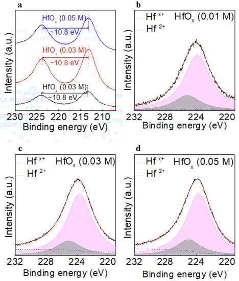
Figure 3.
(a) Hf 4d spectra of HfOx (0.01 M), HfOx (0.03 M), and HfOx (0.05 M) films. Deconvoluted Hf 4d3/2 XPS profiles of the (b) HfOx (0.01 M), (c) HfOx (0.03 M), and (d) HfOx (0.05 M) films.
Figure 4a−d shows the deconvoluted V 2p3/2 XPS profiles for the V2O5, and HfOx (0.01, 0.03, and 0.05 M)/V2O5 films, respectively. The V 2p3/2 spectrum was deconvoluted into two peaks centered at the higher and lower binding energies of ~517.7 eV and ~516.6 eV, respectively. The peak centered at the higher of these two values indicates the V in V5+, whereas the peak centered at the lower value indicates the V in V4+ [23]. Because the V4+ state forms a hole transport channel near the Fermi level, it is necessary to clarify the concentration of V4+ in the V2O5 film [16]. The concentration of V4+ in V2O5, and in the HfOx (0.01, 0.03, and 0.05 M)/V2O5 films was 23.13, 24.59, 26.00, and 25,49%; thus, the HfOx (0.03 M)/V2O5 film had the highest concentration of V4+. During the formation of the V2O5 layer above the oxygen−deficient HfOx layer, the oxygen can diffuse from V2O5 to HfOx because of the difference in the oxygen density between V2O5 and HfOx. This indicates that the highest V4+ concentration of HfOx (0.03 M)/V2O5 could be the consequence of the existence of the highest concentration of oxygen vacancies in HfOx (0.03 M) film [24].
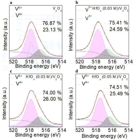
Figure 4.
Deconvoluted V 2p3/2 XPS results of the (a)V2O5, (b) HfOx (0.01 M)/V2O5, (c) HfOx (0.03 M)/V2O5, and (d) HfOx (0.05 M)/V2O5 films.
Figure 5 shows the schematic interfacial energy band diagram of the QLEDs with the aligned Fermi level corresponding to the UPS results and the Tauc plot. The V4+−related gap states of V2O5 near the Fermi level are shown in Figure 5a–d. In the case of HfOx, Hadacek et al. and Hildebrandt et al. reported that the oxygen−deficient HfOx films exhibit p−type behavior. In addition, Kaisar et al. revealed that the origin of the p−type conductivity of oxygen−deficient HfOx is due to the oxygen vacancy−related defect states, which are located ~3 eV above the VBM [25,26,27]. Because of the high concentration of Hfx+ in our HfOx films representative of the large amount of oxygen vacancies in the HfOx films, we indicated that the oxygen−related defect states of HfOx are located 3 eV above the VBM. Therefore, as shown in Figure 5, all the devices containing the HfOx layer would be expected to exhibit enhanced hole injection characteristics owing to the lowered hole injection barrier. In addition, because the device with the HfOx (0.03 M) layer has the lowest hole injection barrier of 0.18 eV at the HfOx/V2O5 interface, the device with the HfOx (0.03 M) layer would be predicted to exhibit the optimal hole injection characteristics.
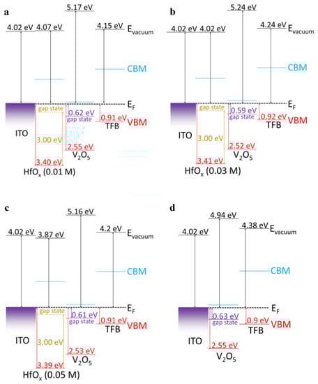
Figure 5.
Schematic energy level diagram of QLEDs (a) without the HfOx layer, and with the (b) HfOx (0.01 M), (c) HfOx (0.03 M), and (d) HfOx (0.05 M) layer.
To corroborate the abovementioned results, we first recorded the current density−voltage (J−V) curves of the hole only devices (HODs) with the structure ITO/(HfOx)/V2O5/TFB/Al as shown in Figure 6a−b. The HOD without the HfOx film had the lowest current density, with that of the HfOx (0.01 M) film being slightly higher. The HOD with the HfOx (0.03 M) film had the highest current density. Considering the alignment of the interfacial energy bands, as shown in Figure 5, the enhanced current density of the HOD can be attributed to the well−aligned gap states between the HfOx and V2O5 layers. Moreover, taking into account that the HfOx (0.03 M)/V2O5 film contains the highest concentration of gap states, originating from the V4+ state, the well−aligned energy levels and the concentration of gap states can both contribute to efficient hole injection. Figure 6c shows the current density−voltage−luminance (J−V−L) characteristics of the QLEDs with and without the HfOx (0.01, 0.03, and 0.05 M) layer. Consistent with the aforementioned improved hole injection characteristics, the QLED with the HfOx (0.03 M) layer had the highest luminance of 166,670 cd/m2, more than twice as high as the QLED without the HfOx layer. In terms of the current density, the device without the HfOx layer had higher values compared with the devices with the HfOx layer. This can be attributed to the high conduction band offset between HfOx and V2O5, which would have efficiently blocked the leakage current toward the ITO. Owing to the diminished leakage current and enhanced hole injection characteristics, the current efficiency (CE) and external quantum efficiency (EQE) of QLEDs with the HfOx (0.03 M) layer increased considerably, as shown in Figure 6c,d. The device with the HfOx (0.03 M) layer exhibited CE and EQE values of 16.6 cd/A and 3.68%, which is more than two−fold higher than the 7.37 cd/A and 1.64% of the device without the HfOx layer. Figure 6e shows the electroluminescence (EL) spectra of the QLED devices with the HfOx (0.01 M), HfOx (0.03 M), and HfOx (0.05 M) layers, and without the HfOx layer at the maximum luminance of each of these devices. The operating image of the QLED is shown in the inset of Figure 6e. All the QLEDs had an emission peak with full width at half maximum (FWHM) of ~25 nm without significant peak shift, indicating that the devices exhibited high color purity. To identify the stability of the device, the lifetime was confirmed at which the luminance reached half of the initial value with the initial luminance discussed, as shown in Figure 6f. The initial luminance values of the devices without HfOx and with HfOx (0.03 M) were 2320.2 and 2535.9 cd/m2, respectively. The lifetimes of the devices at an L0 = 100 cd/m2 was obtained using the following equation
where n is the acceleration factor (1.514), L0 is the initial luminance, L is the luminance, and T50 is the time which the luminance reached the half of the initial luminance value [22]. The longer lifetime of 139 h was obtained by adding HfOx (0.03 M) layer, compared with the 75.9 h of the device without HfOx layer.
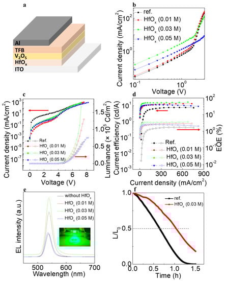
Figure 6.
(a) Schematic illustration of the device fabrication process (b) J−V characteristics of HOD devices. (c) J−V−L characteristics and (d) current efficiency−current density plot of the QLED devices. (e) EL spectra of the QLED devices at each maximum luminance. (f) Lifetime data of the QLED devices without and with HfOx (0.03 M) layer.
4. Conclusions
We fabricated QLEDs with highly enhanced light−emitting characteristics by adding a solution−processed HfOx interfacial layer. The defect states of the HfOx layer, originating from the large amount of oxygen vacancies, could be well−aligned with the gap state of V2O5, resulting in lowering the hole injection barrier from ITO to V2O5. Furthermore, the oxygen−deficient HfOx film also contributed to the increase in the formation of the V4+ state in the V2O5 layer, resulting in enhanced hole injection characteristics. Owing to the improved hole injection characteristics, the device with the optimal HfOx concentration had the highest luminance of 166,670 cd/m2, current efficiency of 16.6 cd/m2, and EQE of 3.68% compared with the values of 63,673 cd/m2, 7.37 cd/A, and 1.64%, respectively, for the device without HfOx layer. UPS and XPS measurements enabled us to identify the origin of the enhanced light−emitting characteristics of the devices. Our results indicate that we developed a useful and facile method for improving the hole injection characteristics of QLEDs by incorporating a solution−processable HfOx interfacial layer.
Author Contributions
J.H.J. and S.J.K. (Seong Jun Kang) planned the experimental details. J.H.J. contributed the fabrication of the devices and analyzing the measured data. M.-J.M., Y.P. and Y.D.K. contributed UPS measurement. M.G.K., J.H.M., H.J.H., M.H.P. and S.J.K.(Seong Jae Kang) conducted the experimental analysis. J.H.J. drafted the manuscript. S.J.K. (Seong Jun Kang) revised and confirmed the manuscript. All authors reviewed the manuscript. All authors have read and agreed to the published version of the manuscript.
Funding
This work was supported by a grant from Kyung Hee University (KHU-20181299).
Institutional Review Board Statement
Not applicable.
Informed Consent Statement
Not applicable.
Data Availability Statement
Data will be made available from the corresponding authors on reasonable request.
Conflicts of Interest
The authors declare no conflict of interest.
References
- Moon, H.; Lee, C.; Lee, W.; Kim, J.; Chae, H. Stability of Quantum Dots, Quantum Dot Films, and Quantum Dot Light−Emitting Diodes for Display Applications. Adv. Mater. 2019, 31, 1804294. [Google Scholar] [CrossRef] [PubMed]
- Zhang, L.; Sun, C.; He, T.; Jiang, Y.; Wei, J.; Huang, Y.; Yuan, M. High−Performance Quasi−2D Perovskite Light−Emitting Diodes: From Materials to Devices. Light Sci. Appl. 2021, 10, 61. [Google Scholar] [CrossRef] [PubMed]
- Ji, K.; Anaya, M.; Abfalterer, A.; Stranks, S.D. Halide Perovskite Light−Emitting Diode Technologies. Adv. Opt. Mater. 2021, 9, 2002128. [Google Scholar] [CrossRef]
- Sudheendran Swayamprabha, S.; Dubey, D.K.; Shahnawaz; Yadav, R.A.K.; Nagar, M.R.; Sharma, A.; Tung, F.; Jou, J. Approaches for Long Lifetime Organic Light Emitting Diodes. Adv. Sci. 2020, 8, 2002254. [Google Scholar] [CrossRef]
- Cheng, Y.; Wan, H.; Liang, T.; Liu, C.; Wu, M.; Hong, H.; Liu, K.; Shen, H. Continuously Graded Quantum Dots: Synthesis, Applications in Quantum Dot Light−Emitting Diodes, and Perspectives. J. Phys. Chem. Lett. 2021, 12, 5967–5978. [Google Scholar] [CrossRef]
- Won, Y.-H.; Cho, O.; Kim, T.; Chung, D.-Y.; Kim, T.; Chung, H.; Jang, H.; Lee, J.; Kim, D.; Jang, E. Highly Efficient and Stable InP/ZnSe/ZnS Quantum Dot Light−Emitting Diodes. Nature 2019, 575, 634–638. [Google Scholar] [CrossRef]
- Park, M.; Roh, J.; Lim, J.; Lee, H.; Lee, D. Double Metal Oxide Electron Transport Layers for Colloidal Quantum Dot Light−Emitting Diodes. Nanomaterials 2020, 10, 726. [Google Scholar] [CrossRef]
- Jin, H.; Moon, H.; Lee, W.; Hwangbo, H.; Yong, S.H.; Chung, H.K.; Chae, H. Charge Balance Control of Quantum Dot Light Emitting Diodes with Atomic Layer Deposited Aluminum Oxide Interlayers. RSC Adv. 2019, 9, 11634–11640. [Google Scholar] [CrossRef]
- Wang, F.; Sun, W.; Liu, P.; Wang, Z.; Zhang, J.; Wei, J.; Li, Y.; Hayat, T.; Alsaedi, A.; Tan, Z. Achieving Balanced Charge Injection of Blue Quantum Dot Light−Emitting Diodes through Transport Layer Doping Strategies. J. Phys. Chem. Lett. 2019, 10, 960–965. [Google Scholar] [CrossRef]
- Jin, X.; Chang, C.; Zhao, W.; Huang, S.; Gu, X.; Zhang, Q.; Li, F.; Zhang, Y.; Li, Q. Balancing the Electron and Hole Transfer for Efficient Quantum Dot Light−Emitting Diodes by Employing a Versatile Organic Electron−Blocking Layer. ACS Appl. Mater. Interfaces 2018, 10, 15803–15811. [Google Scholar] [CrossRef]
- Zhang, N.; Qu, X.; Lyu, Q.; Wang, K.; Sun, X.W. Highly Efficient Transparent Quantum−Dot Light−Emitting Diodes Based on Inorganic Double Electron−Transport Layers. Photonics Res. 2021, 9, 1979–1983. [Google Scholar] [CrossRef]
- Sun, Y.; Chen, W.; Wu, Y.; He, Z.; Zhang, S.; Chen, S. A Low−Temperature−Annealed and UV−Ozone−Enhanced Combustion Derived Nickel Oxide Hole Injection Layer for Flexible Quantum Dot Light−Emitting Diodes. Nanoscale 2019, 11, 1021–1028. [Google Scholar] [CrossRef] [PubMed]
- Dhar, S.; Chakraborty, P.; Majumder, T.; Mondal, S.P. Acid−Treated PEDOT:PSS Polymer and TiO2 Nanorod Schottky Junction Ultraviolet Photodetectors with Ultrahigh External Quantum Efficiency, Detectivity, and Responsivity. ACS Appl. Mater. Interfaces 2018, 10, 41618–41626. [Google Scholar] [CrossRef] [PubMed]
- Lee, J.H.; Jeong, Y.R.; Lee, G.; Jin, S.W.; Lee, Y.H.; Hong, S.Y.; Park, H.; Kim, J.W.; Lee, S.-S.; Ha, J.S. Highly Conductive, Stretchable, and Transparent PEDOT:PSS Electrodes Fabricated with Triblock Copolymer Additives and Acid Treatment. ACS Appl. Mater. Interfaces 2018, 10, 28027–28035. [Google Scholar] [CrossRef] [PubMed]
- Shin, J.S.; Kim, M.; Ma, J.H.; Jeong, J.H.; Hwang, H.W.; Kim, J.W.; Kang, S.J. Solution−processable Li−doped transition metal oxide hole−injection layer for highly efficient quantum−dot light−emitting diodes. J. Mater. Chem. C 2022, 10, 5590–5597. [Google Scholar] [CrossRef]
- Heo, S.B.; Yu, J.H.; Shin, J.S.; Kim, T.Y.; Kim, B.S.; Jeon, W.; Kang, S.J. Effect of Inorganic Interfacial Modification Layer on the Performance of Quantum−Dots Light−Emitting Diodes. Jpn. J. Appl. Phys. 2020, 59, 124002. [Google Scholar] [CrossRef]
- Shin, J.S.; Kim, T.Y.; Heo, S.B.; Hong, J.-A.; Park, Y.; Kang, S.J. Improving the Performance of Quantum−Dot Light−Emitting Diodes via an Organic–Inorganic Hybrid Hole Injection Layer. RSC Adv. 2021, 11, 4168–4172. [Google Scholar] [CrossRef]
- Kim, T.Y.; Park, S.; Kim, B.J.; Heo, S.B.; Yu, J.H.; Shin, J.S.; Hong, J.-A.; Kim, B.-S.; Kim, Y.D.; Park, Y.; et al. Dual−Functional Quantum−Dots Light Emitting Diodes Based on Solution Processable Vanadium Oxide Hole Injection Layer. Sci. Rep. 2021, 11, 1700. [Google Scholar] [CrossRef]
- Park, S.; Kim, B.J.; Kang, S.J.; Cho, N.-K. Photocurrent Characteristics of Zinc−Oxide Films Prepared by Using Sputtering and Spin−Coating Methods. J. Korean Phys. Soc. 2018, 73, 1351–1355. [Google Scholar] [CrossRef]
- Selvakumar, N.; Barshilia, H.C.; Rajam, K.S.; Biswas, A. Structure, Optical Properties and Thermal Stability of Pulsed Sputter Deposited High Temperature HfOx/Mo/HfO2 Solar Selective Absorbers. Sol. Energy Mater. Sol. Cells 2010, 94, 1412–1420. [Google Scholar] [CrossRef]
- Paul, A.D.; Biswas, S.; Das, P.; Edwards, H.J.; Dalal, A.; Maji, S.; Dhanak, V.R.; Mondal, A.; Mahapatra, R. Improved Resistive Switching Characteristics of Ag/Al:HfOx/ITO/PET ReRAM for Flexible Electronics Application. Semicond. Sci. Technol. 2021, 36, 065006. [Google Scholar] [CrossRef]
- Kim, M.G.; Shin, J.S.; Ma, J.H.; Jeong, J.H.; Han, D.H.; Kim, B.-S.; Jeon, W.; Park, Y.; Kang, S.J. An Al−Doped TiO2 Interfacial Layer for Effective Hole Injection Characteristics of Quantum−Dot Light−Emitting Diodes. J. Mater. Chem. C 2022, 10, 7294–7303. [Google Scholar] [CrossRef]
- Narayanan, R.; Dewan, A.; Chakraborty, D. Complimentary Effects of Annealing Temperature on Optimal Tuning of Functionalized Carbon–V2O5 Hybrid Nanobelts for Targeted Dual Applications in Electrochromic and Supercapacitor Devices. RSC Adv. 2018, 8, 8596–8606. [Google Scholar] [CrossRef] [PubMed]
- Kita, K.; Toriumi, A. Origin of Electric Dipoles Formed at High−k/SiO2 Interface. Appl. Phys. Lett. 2009, 94, 132902. [Google Scholar] [CrossRef]
- Hadacek, N.; Nosov, A.; Ranno, L.; Strobel, P.; Galéra, R.-M. Magnetic Properties of HfO2Thin Films. J. Phys. Condens. Matter 2007, 19, 486206. [Google Scholar] [CrossRef]
- Hildebrandt, E.; Kurian, J.; Müller, M.M.; Schroeder, T.; Kleebe, H.-J.; Alff, L. Controlled Oxygen Vacancy Induced p−Type Conductivity in HfO2−x Thin Films. Appl. Phys. Lett. 2011, 99, 112902. [Google Scholar] [CrossRef]
- Kaiser, N.; Vogel, T.; Zintler, A.; Petzold, S.; Arzumanov, A.; Piros, E.; Eilhardt, R.; Molina−Luna, L.; Alff, L. Defect−Stabilized Substoichiometric Polymorphs of Hafnium Oxide with Semiconducting Properties. ACS Appl. Mater. Interfaces 2021, 14, 1290–1303. [Google Scholar] [CrossRef]
Publisher’s Note: MDPI stays neutral with regard to jurisdictional claims in published maps and institutional affiliations. |
© 2022 by the authors. Licensee MDPI, Basel, Switzerland. This article is an open access article distributed under the terms and conditions of the Creative Commons Attribution (CC BY) license (https://creativecommons.org/licenses/by/4.0/).