Article

Near-Infrared Artificial Optical Synapse Based on the P(VDF-TrFE)-Coated InAs Nanowire Field-Effect Transistor

1
Key Laboratory for the Physics and Chemistry of Nanodevices, School of Electronics, Peking University, Beijing 100871, China
2
Academy for Advanced Interdisciplinary Studies, Peking University, Beijing 100871, China
*
Author to whom correspondence should be addressed.
Materials 2022, 15(22), 8247; https://doi.org/10.3390/ma15228247
Submission received: 22 September 2022 / Revised: 27 October 2022 / Accepted: 8 November 2022 / Published: 21 November 2022
(This article belongs to the Special Issue III-V Nanostructures and Their Devices)

Abstract

:
Optical synapse is the basic component for optical neuromorphic computing and is attracting great attention, mainly due to its great potential in many fields, such as image recognition, artificial intelligence and artificial visual perception systems. However, optical synapse with infrared (IR) response has rarely been reported. InAs nanowires (NWs) have a direct narrow bandgap and a large surface to volume ratio, making them a promising material for IR detection. Here, we demonstrate a near-infrared (NIR) (750 to 1550 nm) optical synapse for the first time based on a poly(vinylidene fluoride-trifluoroethylene) (P(VDF-TrFE))-coated InAs NW field-effect transistor (FET). The responsivity of the P(VDF-TrFE)-coated InAs NW FET reaches 839.3 A/W under 750 nm laser illumination, demonstrating the advantage of P(VDF-TrFE) coverage. The P(VDF-TrFE)-coated InAs NW device exhibits optical synaptic behaviors in response to NIR light pulses, including excitatory postsynaptic current (EPSC), paired-pulse facilitation (PPF) and a transformation from short-term plasticity (STP) to long-term plasticity (LTP). The working mechanism is attributed to the polarization effect in the ferroelectric P(VDF-TrFE) layer, which dominates the trapping and de-trapping characteristics of photogenerated holes. These findings have significant implications for the development of artificial neural networks.

1. Introduction

With the continuous advancement of semiconducting technology, traditional von Neumann architectures are confronting extreme bottlenecks in processing speed and energy consumption [1,2]. Neuromorphic computing is a newly computing architecture attempting to overcome the limitations of von Neuman-based computing [3,4]. Light has been widely used as a communication medium in telecoms and data centers. Infrared (IR) light detection is especially important in biomedical imaging, communications engineering and machine vision [5,6,7]. However, few materials can achieve wide-spectrum infrared detection because many materials have large band gaps. Besides, light is expected to play a significant part in high-speed real-time artificial neuromorphic computing with low latency, low power consumption, and high bandwidth [8]. Various optical synaptic devices have been developed as essential components of optical neuromorphic systems [9]. Controlling the relaxation properties of photogenerated carriers is crucial for the realization of optical synapses, since the photocurrent can be sustained for a long period after illumination, thereby providing memory features for the simulation of synapse functions [10,11]. To this end, many optical synaptic devices have been designed on different principles, including those based on phase-change materials [12,13], memristors [14,15], ferroelectrics [16,17,18,19], charge trapping/de-trapping [20,21,22,23] or ion transport mechanisms [24].
Synaptic behaviors under light stimulation have been simulated using various materials, such as nanowires (NWs) [25,26], Si nanocrystals (NCs) [27,28], oxide semiconductors [29,30], two-dimensional materials [17,31,32,33,34,35], indium arsenide (InAs) dots [36], hybrid perovskites [37,38], and organic materials [19,39,40,41]. The basic synaptic functions, such as excitatory postsynaptic current (EPSC)/inhibitory postsynaptic current (IPSC), paired-pulse facilitation (PPF), and short-term plasticity (STP)/long-term plasticity (LTP), have been simulated using light stimuli [9,42]. Unfortunately, most of the current optical synaptic devices can only work in the ultraviolet-visible light region, while the IR optical synaptic device has rarely been reported based on organic/inorganic materials. InAs NWs have a direct narrow bandgap ( ~ 0.35 eV) naturally providing significant advantages in IR detection [43,44]. Although InAs NW optical synaptic devices have been demonstrated in the UV and visible light region [21,45], there have been no reports on InAs NW optical synapse in IR region.
Here, we present an InAs NW IR optical synaptic device in the near-infrared (NIR) range (750 to 1550 nm) for the first time with the help of ferroelectric material poly(vinylidene fluoride-trifluoroethylene) (P(VDF-TrFE)) coverage. The functions of optical synaptic devices, such as EPSC, PPF, and STP/LTP, are demonstrated by light stimulus.

2. Materials and Methods

2.1. Nanowire Growth and Device Fabrication

High-quality single-crystalline InAs NWs were synthesized by metal–organic chemical vapor deposition (MOCVD). The detailed growth process and characterization have been reported in our previous work [46]. The as-grown InAs NWs were transferred and uniformly dispersed onto a heavily p-doped Si substrate covered by a 300 nm-thick SiO2. After the electrodes were patterned by electron-beam lithography, the surface oxide layer outside InAs NW in the contact area was removed by (NH4)Sx solution before the metal deposition to ensure ohmic contact between the metal electrodes and InAs NW. A double-layer metal Ti/Au with a thickness of 5/90 nm was deposited on the surface of InAs NW by electron beam evaporation and liftoff. P(VDF-TrFE) (70:30 in mol%) thin films were spin-coated on the channel of the device and then annealed at 130 °C for 30 min to crystallize. The detailed device fabrication process is the same as that in the previous reports by our group [46].

2.2. Characterization and Measurement

High-resolution transmission electron microscopy (HRTEM) is used to characterize the lattice quality of InAs NW in a Tecnai F20 TEM (FEI, Portland, OR, USA). The morphology of InAs NWs on the transferred substrate are observed and positioned by scanning electron microscopy (SEM) (using a Quanta FEG 600, FEI, Brno, Czech Republic), and the diameter of the NW is measured by atomic force microscopy (AFM) (using a Multimode 8 system, Bruker, Karlsruhe, Germany). All optoelectrical measurements are carried out in air at room temperature on a LabRAM HR800 evolution system (Horiba Jobin-Yvon, Paris, France) with NKT EXR-15 supercontinuum laser sources. Simultaneous optoelectrical characterization was performed using a Keithley 4200 semiconductor analyzer (Keithley, Cleveland, OH, USA) equipped with a probe station. The detailed optoelectrical measurements can be found in the previous report by our group [47].

3. Results and Discussion

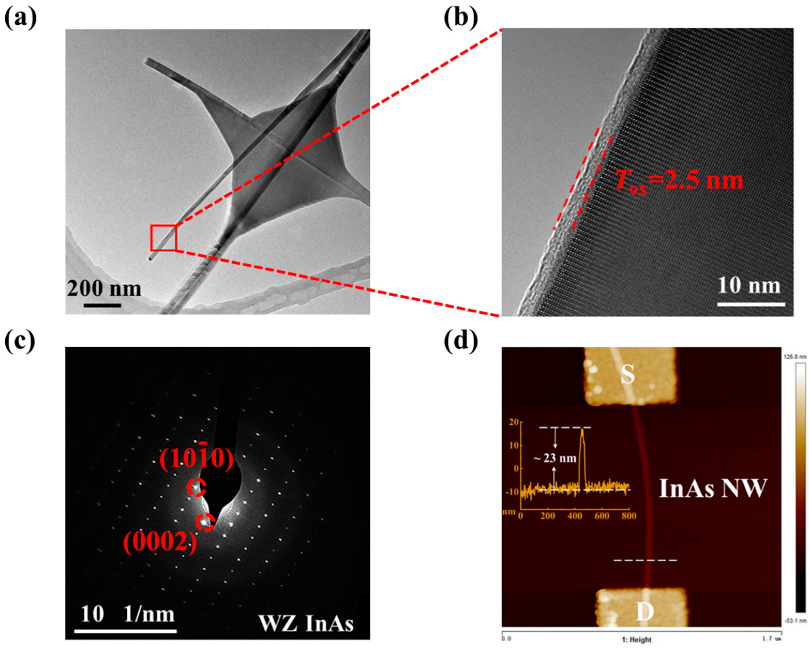
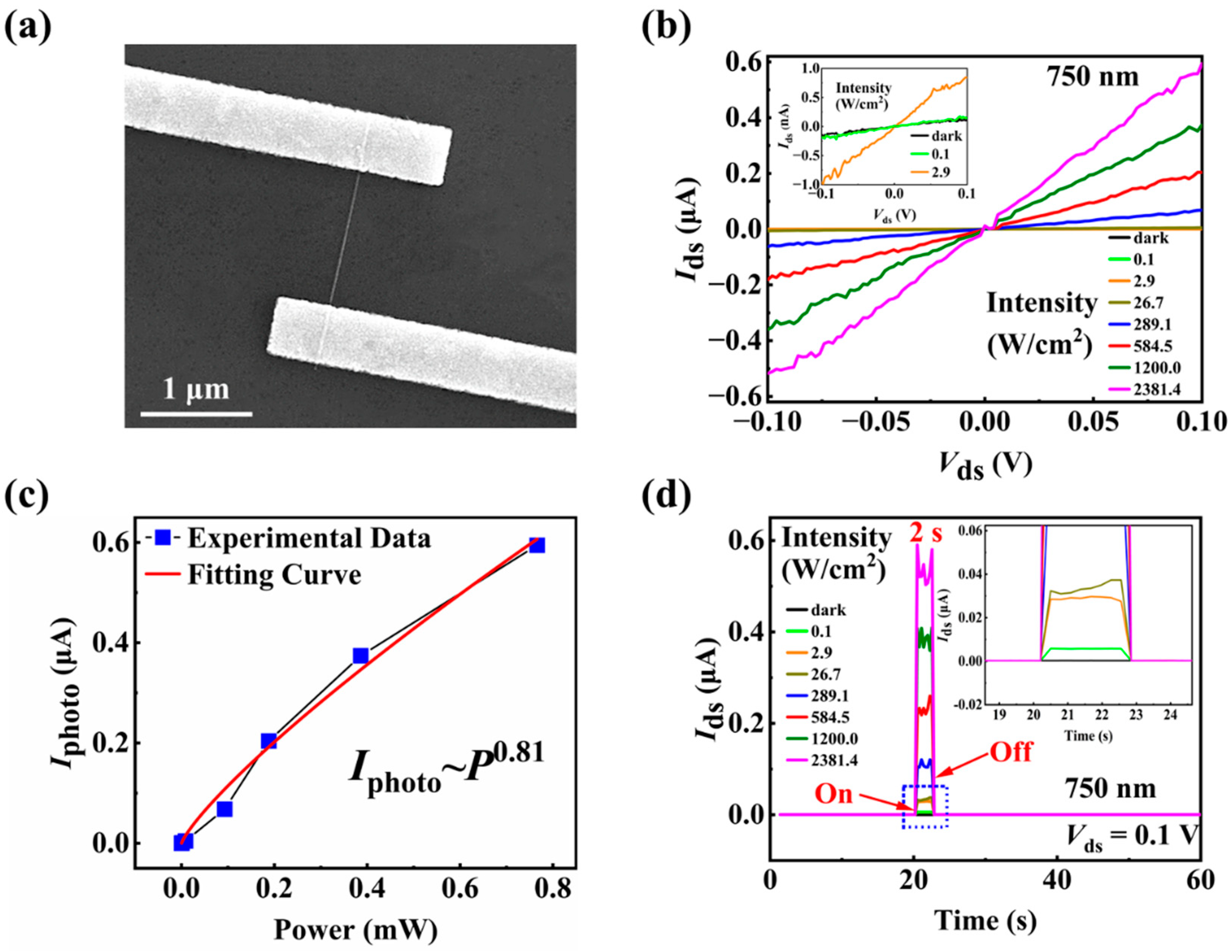
3.1. The Pristine InAs NW Device Optoelectronic Properties

Figure 1a is a transmission electron microscopy (TEM) image of the NWs, indicating that the NWs have smooth surface and uniform diameter. Figure 1b,c are the high-resolution TEM (HRTEM) image and electron diffraction pattern, respectively, showing the NW has a wurtzite (WZ) structure with the axis along the [0001] direction and is covered by a 2.5 nm native oxide layer due to the exposure to air after the growth. Before depositing the Ti/Au = 5/90 nm electrodes, the oxide layer in the contact area was etched by (NH4)Sx solution for 90 s to ensure ohmic contact. The scanning electron microscopy (SEM) image of a typical InAs NW field-effect transistor (FET) is shown in Figure 2a. The channel length of the device is 1.2 μm, and the diameter of the NW (with the native oxide layer) is measured to be 23 nm by atomic force microscopy (AFM), as shown in Figure 1d.
Before investigating the optoelectronic properties of the device, the electrical properties of the InAs NW FETs are measured. The p-type heavily doped Si substrate is used as the back-gate, and the 300 nm SiO2 layer is used as the back-gate dielectric layer. The output and transfer characteristic curves of the as-fabricated back-gate device (the pristine device) are measured at room temperature. The output characteristics are shown in Figure 3a. The source-drain current (Ids) increases linearly with the source-drain voltage (Vds) at the beginning and tends to saturate at large Vds for different gate voltages (Vgs). Such phenomena confirm good ohmic contact in the device due to the Fermi level pinning near the bottom of the conductance band of InAs [48]. The transfer curve of the device is shown in Figure 3b. During the measurement, a scanning voltage of −10 V to 10 V is applied to the gate, and a fixed bias voltage Vds of 0.1 V is applied between the source and drain electrodes. The device shows an n-type characteristic with a high on/off ratio of ≈105 in a Vgs sweeping range of −10 V to 10 V, as shown in Figure 3b. The field-effect mobility ( μ ) can be extracted using the following equation [49,50]:
μ = g L g 2 C ox V ds
where g is the transconductance (calculated from the measured transfer curve using g = dIds/dVgs), Lg is the gate length, C OX is the gate oxide capacitance of the devices and can be calculated using C OX = 2 π ε 0 ε r / cos h [ ( t ox + r NW ) / r NW ] , where ε 0 is the vacuum permittivity, ε r is the relative permittivity of the dielectric, t ox is the thickness of the gate oxide layer, and r NW is the radius of InAs NW. The field-effect mobility is calculated to be 1116 cm2/V·s from the measured transfer curve, which is comparable to the previously reported field-effect mobilities in InAs NW FETs at room temperature [51].
The optoelectronic properties of InAs NW FETs are measured in air at room temperature and at Vgs = 0 V unless otherwise specified. As shown in the inset of Figure 2b, the dark current Idark, referring to the Ids without light illumination, has an ultralow value of 0.1 nA at Vds = 0.1 V, which is close to that of the latest reported NW-based advanced photodetector [52,53]. A positive photoconductive effect with highly sensitive photodetection is observed under 750 nm light illumination. Even when the light intensities are as low as 0.1 W/cm2, the current of the device under 750 nm laser illumination is greater than that in the dark. Figure 2b displays the current of the pristine device increases from 0.18 nA to 0.6 μA at Vds = 0.1 V as the intensity of the 750 nm light increases from 0.1 to 2381.4 W/cm2. The current on/off ratio of the device is about 6 × 10³ for the light with the intensity of 2381.4 W/cm2 at Vds = 0.1 V. In Figure 2c, the photocurrent (Iphoto, defined as the difference of the current under light illumination and in the dark) at Vds = 0.1 V increases nonlinearly with the incident light power. In previous works, the relationship between experimental photocurrent and incident light power has been fitted with a power function, which reflects the generation mechanism of photocurrent under light illumination [54]. Hence, we also fit the experimental data using the equation of Iphoto~Pm, where m is the exponent of the power function and P is the incident light power, respectively. When m approaches 1, it means that the generation-recombination process is the main origin of the photocurrent. However, a value of m less than 1 is generally observed, which indicates that the photoelectric conversion process contains complex mechanisms, including electron-hole generation, recombination and trapping [55]. Here, in the present InAs NW optical synapse, the fitting value m is 0.81, which indicates that the defect trapping process contributes to the photocurrent a lot. Figure 2d shows the time-resolved current response to the 750 nm light pulses with different light intensities. It shows clearly that after the light is switched off, the current quickly returns to the initial current value, indicating the pristine InAs NW device does not have synaptic characteristics.

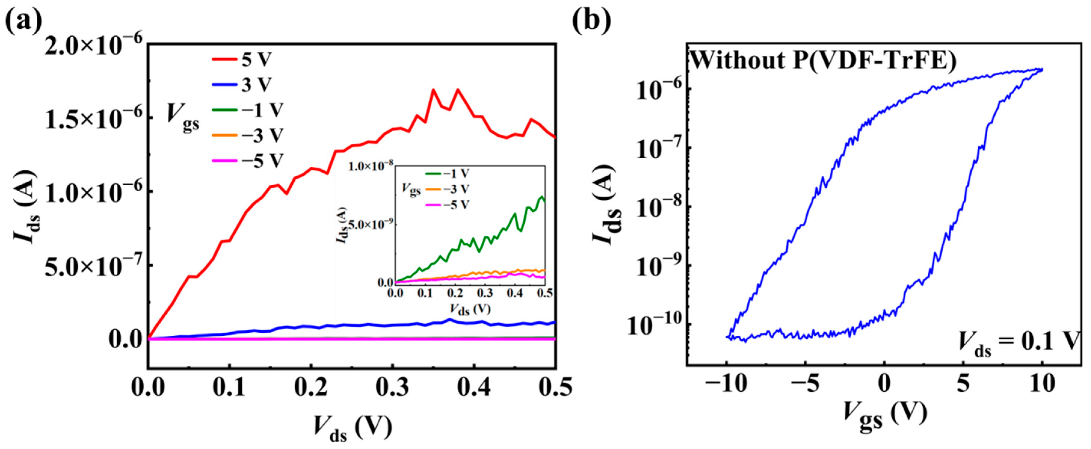
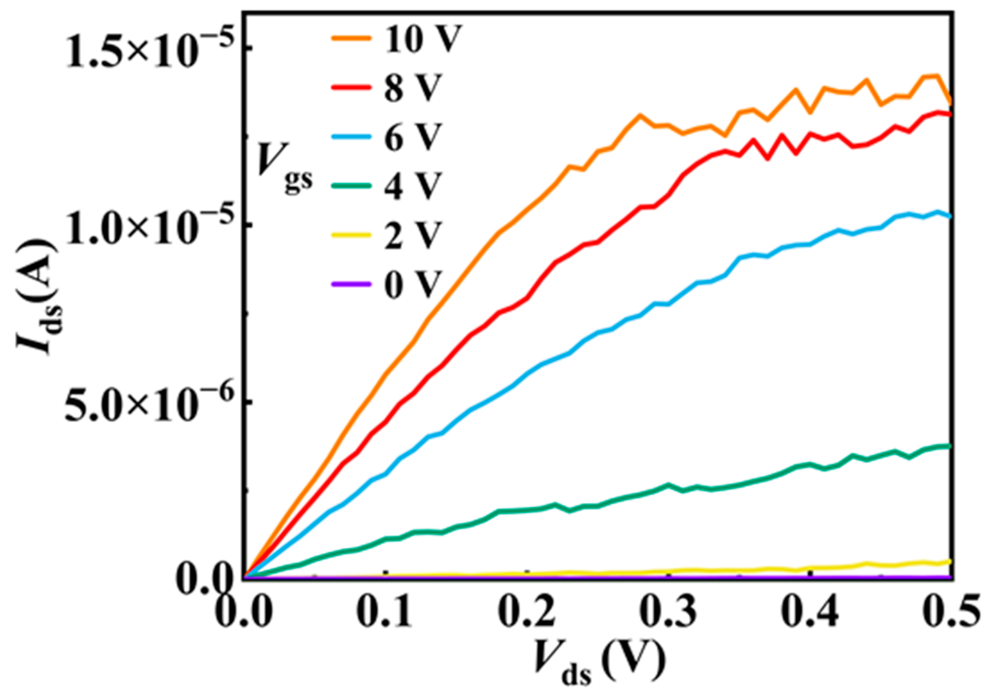
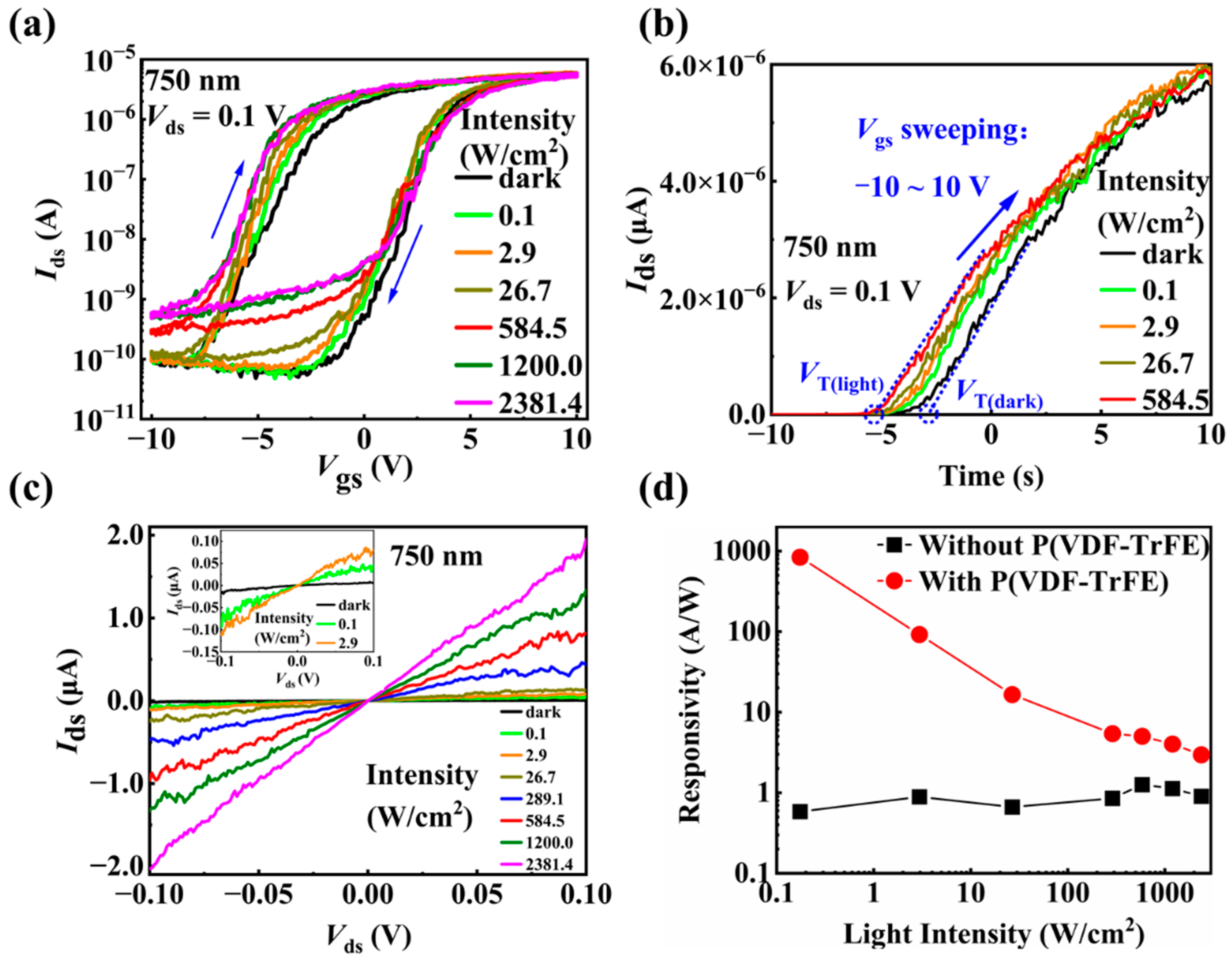
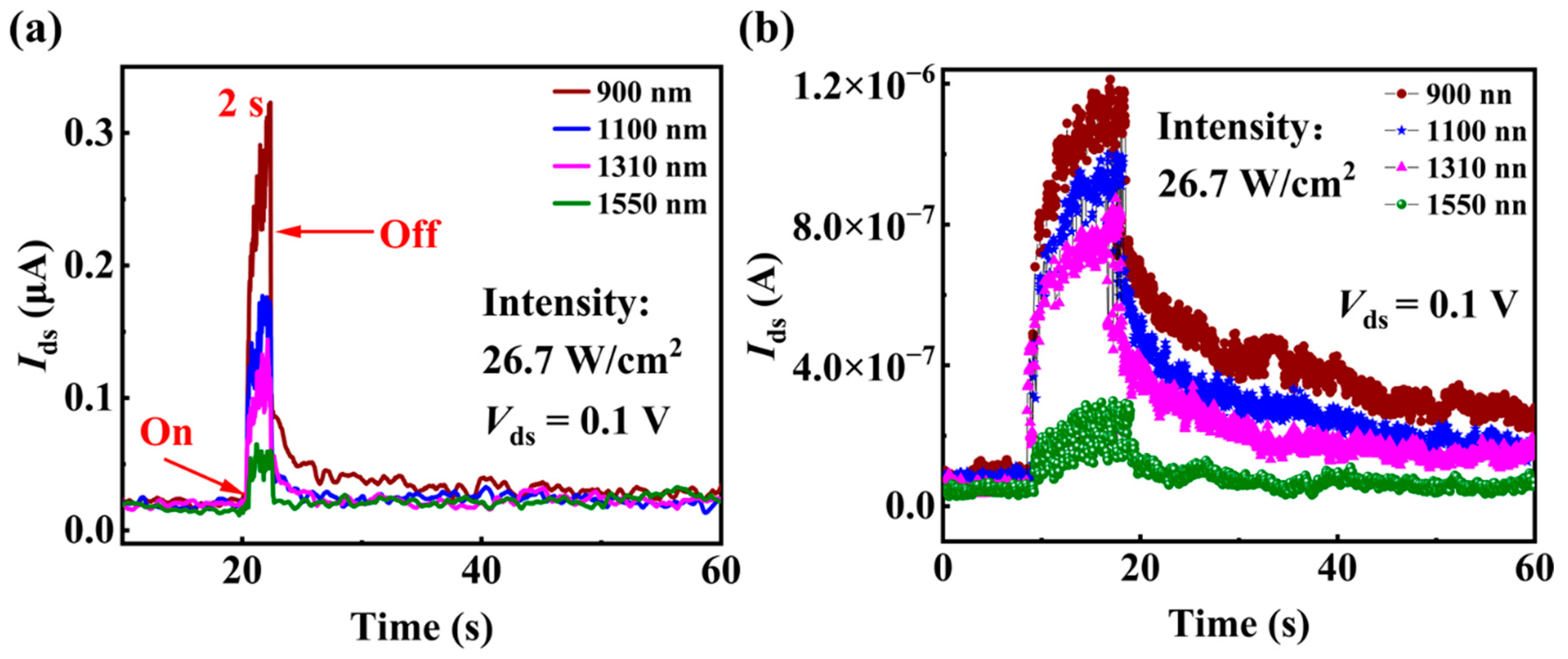
3.2. The P(VDF-TrFE)-Coated InAs NW Device Optoelectronic Properties

Recently, we have found that ferroelectric polymer P(VDF-TrFE) coating not only significantly improves the electrical performance of InAs NW FETs but also enables a very good electrical synaptic behavior of the devices [56]. We therefore study here whether the P(VDF-TrFE) coating can improve the optoelectronic performance of the device or even induce optical synaptic behaviors in the InAs NW FETs. As can be seen in Figure 4, the output characteristics of the P(VDF-TrFE)-coated InAs NW FET display an on-state current of 14.2 μA at Vds = 0.5 V, which is much larger than that in the pristine device. Figure 5a shows the transfer curves of the device after the P(VDF-TrFE) coating in the dark and under the illumination of 750 nm laser. The transfer curves do not coincide when the gate voltage scans from −10 V to 10 V and from 10 V to −10 V, as shown in Figure 5a, indicating that there is a hysteresis in the transfer curves. The hysteresis, corresponding to the storage window, increases as the light intensity increases, also shown in Figure 5a. We use the threshold voltage, VT, to quantitatively describe the hysteresis in the transfer curves. The VT is measured by elongating the tangent line of the transfer curve in linear scale to intersect with the horizontal axis, the intersection point is the VT value, as shown in Figure 5b. It can be seen in Figure 5b, that the threshold voltage (VT) moves to the left under the light illumination for Vgs sweeping from −10 V to 10 V, and the higher the light intensity, the more the movement. As shown in Figure 5a the transfer curves do not move obviously when Vgs is swept from 10 V to −10 V. Therefore, the hysteresis increases with the light intensity under the illumination of 750 nm light.
After the P(VDF-TrFE) coating, the dark current at Vgs = 0 V increases to 9.6 nA and the photocurrent increases more obviously than that in the pristine device with the same light intensity, as shown in Figure 5c. The P(VDF-TrFE) coating not only reduces surface defects but also enhances the electric field around the NW and increases the performance of the P(VDF-TrFE)-coated InAs NW FET [56], which explains the increase of the dark current. The responsivity (R) of a photodetector is widely used to evaluate the sensitivity of photodetectors and can be calculated as: R = I photo P × A , where P is the incident light intensity and A ( = L × d , where L is the channel length, d is the NW diameter) is the effective irradiation area on the NW [57]. Here, from the experimental values of photocurrent Iphoto under different light intensities extracted from Figure 2b and Figure 5c, the responsivities are obtained for the devices before and after P(VDF-TrFE) coating. Figure 5d compares the responsivity of the device with and without P(VDF-TrFE) coating for different light intensities. It shows that the responsivity of the device after P(VDF-TrFE) coating is greater than that of the pristine device for all the light intensities, demonstrating the benefit of P(VDF-TrFE) coating on improving the photoelectronic performance of the InAs NW devices. The responsivity of the P(VDF-TrFE)-coated device decreases with the increase in the light intensity. The maximum responsivity is obtained to be 839.3 A/W at the lowest light intensity of 0.1 W/cm2 of 750 nm light.

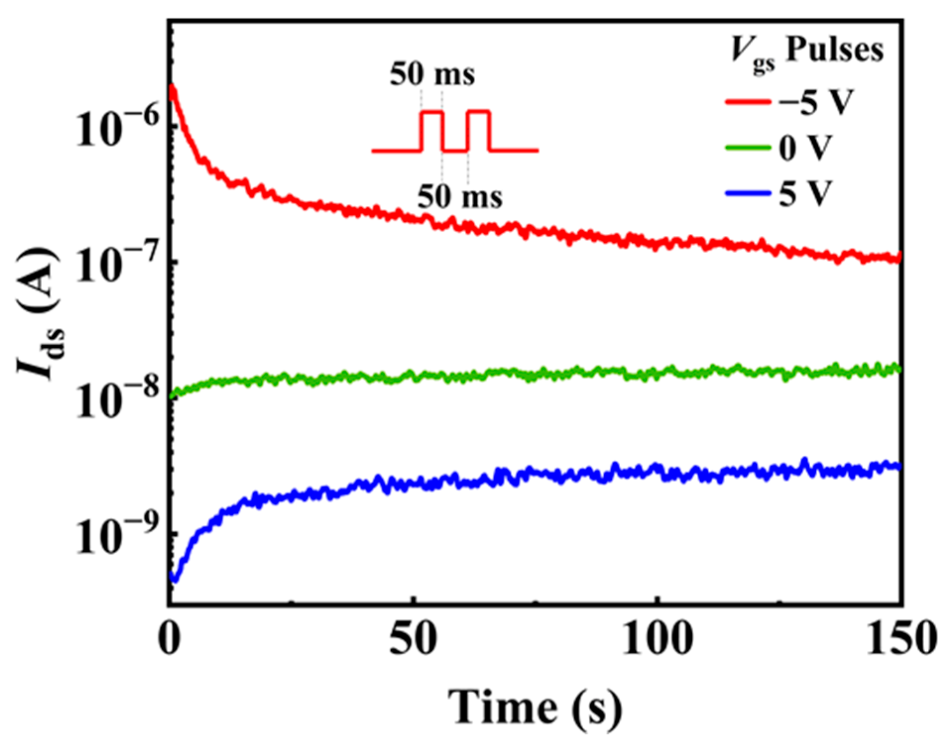
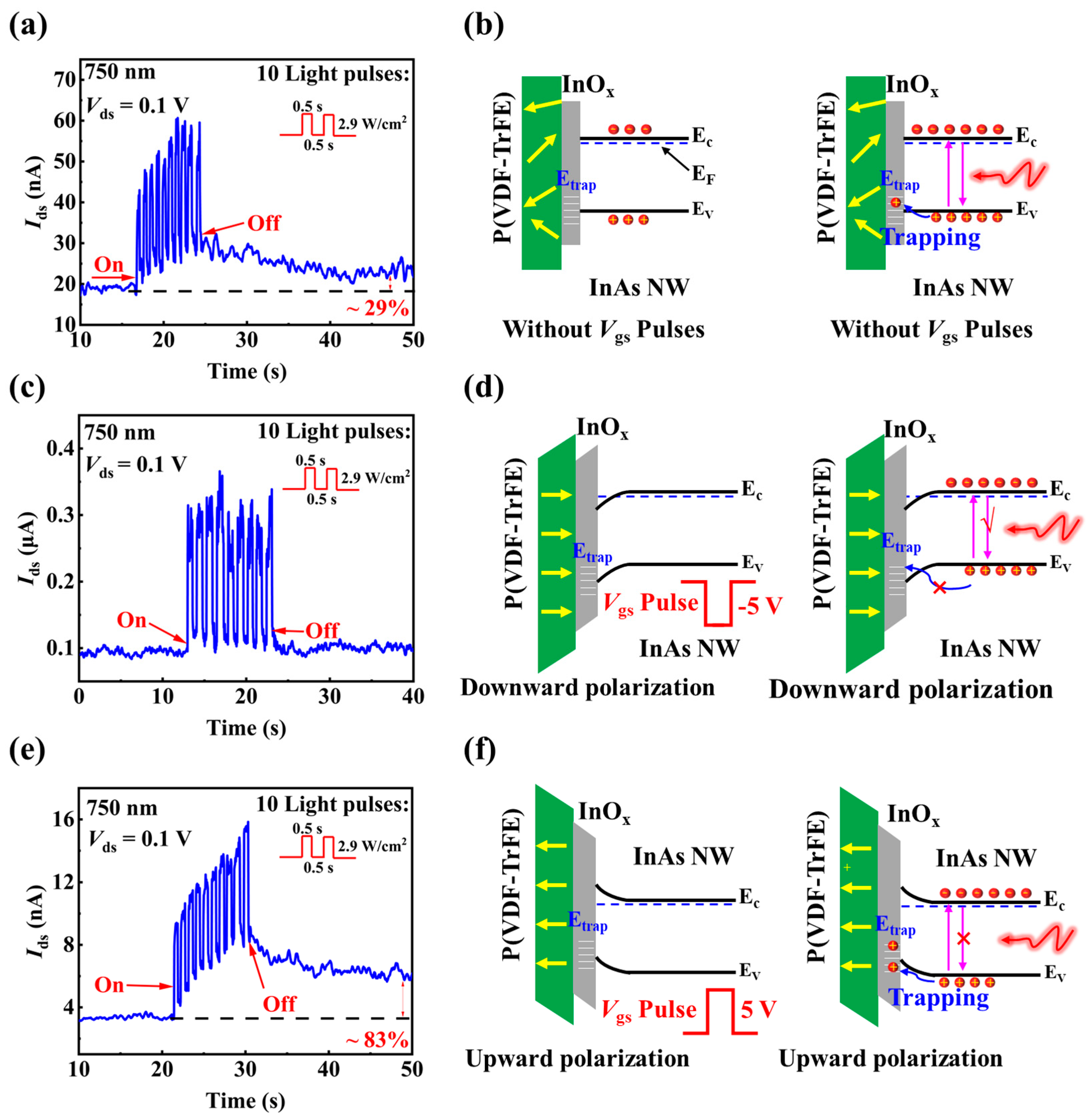
3.3. Optical Synaptic Behavior Based on P(VDF-TrFE)-Coated InAs NW FET

Biological synapses are the basic units for learning, memory, and information processing by human beings. As schematically shown in Figure 6a, the neurotransmitters released by the pre-synapse act on the post-synapse and cause the changes in post-synapse potential in response to various external stimuli [32,58]. To mimic the response of biological synapses to light stimulation, the P(VDF-TrFE)-coated InAs NW FET is regarded as a synapse with light pulses as the presynaptic stimulus. The source and drain electrodes act as the post-synapse. The source-drain current Ids is the EPSC and the channel conductance represents the synaptic weight. Figure 6b shows the current change in a P(VDF-TrFE)-coated InAs NW device after applying individual 750 nm light pulse with different light intensities at Vds = 0.1 V. It displays clearly that the current increases immediately when the light stimuli arrives and then decreases slowly after the light is switched off. The current just after the light pulses (that is EPSC) and the recovery time (the time needed for the current to return to the original dark current value after the light is switched off) increase with the increasing light intensity, exhibiting a typical EPSC behavior similar to a biological synapse. Additionally, when the duration time of the light pulse increases from 0.5 s to 2.0 s, EPSC increases from 0.27 μA to 0.38 μA and the current recovery time also increases, as shown in Figure 6c. Therefore, increasing the intensity or the duration of the light pulse increases both the amplitude of EPSC and the recovery time, successfully simulating a transformation from STP to LTP in biological synapses.
Due to a short-term memory (STM) effect, when a synaptic device is stimulated by two consecutive stimuli, the post-synaptic current caused the second stimulus will be higher than that by the first stimulus, as shown in Figure 6d. Paired-pulse facilitation (PPF) refers to the increases in the ratio between the two post-synaptic currents caused by two consecutive stimuli [21], showing a STM capacity of the synaptic device. It can be seen from Figure 6d that the EPSC after the second light pulse (A2, 0.12 μA) is greater than that after the first light pulse (A1, 0.05 μA) with the same light intensity of 26.7 W/cm2 and the same duration time of 0.2 s, demonstrating a typical PPF behavior. The mechanism of PPF in our device could be that electron-hole pairs are generated in the InAs NW channel by the light illumination. After the first light pulse, some of the photo-generated holes are trapped at the InAs/InOX interface and/or in the InOX layer. If the interval time is short enough, the trapped holes generated during the first light pulse will not be completely released before the second light pulse arrives. Correspondingly, the movable electrons in the InAs NW channel induced by the trapped holes will not be recombined completely, so that the photogenerated carriers generated by the first light pulse do not decay completely. At this moment, the second light pulse arrives and generates more electron-hole pairs. Thus, the post-synaptic current that triggered by the second 750 nm light pulse is larger than the first one. With a longer pulse interval, more trapped holes are released, resulting in a smaller second post-synaptic current.
PPF index, which is defined as the ratio of A 2 A 1 A 1 × 100 % , is used to quantitatively indicate PPF behavior. A1 and A2 are the EPSCs for the first and the second light pulses, respectively, as shown in Figure 6d. In Figure 6e, PPF indices are summarized as the interval time of the two light pulses (with light wavelength of 750 nm, light intensity of 26.7 W/cm2 and duration time of 0.2 s). Part of the original data for Figure 6e are displayed in Figure 7. PPF index is 160% when the interval time is 0.16 s and decreases rapidly with the interval time increasing, suggesting that memory-loss accelerates with increasing interval time. The relationship between PPF index and interval time has been reported to be fitted by a double exponential function of the interval time [42]:
PPF   index = c 1 e Δ t τ 1 + c 2 e Δ t τ 2 + c 0
where Δ t is the interval time of the two consecutive light pulses, c 0 , c 1 and c 2 are characteristic constants, τ 1 and τ 2 correspond to the characteristic time of the fast phase and slow phase, respectively. Through fitting the experimental data in Figure 6e by a double exponential function, two-time constants are obtained to be τ 1 = 0.02 s and τ 2 = 0.23 s, which are similar to those in biological synapse. The values of τ 2 are about one order of magnitude larger than those of τ 1 for the incident laser wavelength of 750 nm, consistent with the decay characteristics of the PPF index in biological synapses [42,59]. The decay in PPF index with interval time could be understood as followed. When the interval time Δ t is apparently smaller than the EPSC decay time, PPF index is rather sensitive to Δ t . PPF index sharply decreases with the increase of Δ t , giving rise to the rapid decay process of PPF index with the characteristic relaxation time of τ 1 . When Δ t is longer than the EPSC decay time, the enhancement of the photocurrent stimulated by the second spike is weakened, so that PPF index decays slowly with the characteristic relaxation time of τ 2 .
In the human body, synaptic plasticity is also closely related to the process of memory formation. STM, which is stored in the hippocampus and easily annihilated by new information, can be consolidated and transformed into long-term memory (LTM) through sustained repetitive practice [60]. Figure 6f shows the EPSCs response to 20 light pulses stimulus (0.5 s duration, 50 ms interval time) of the P(VDF-TrFE)-coated InAs NW device with different light intensities of 750 nm laser. When the light pulses with an intensity of 2.9 W/cm2 are applied, EPSC is 0.2 μA after 20 light pulses, and then decreased slowly. With the increasing number of the light pulses, EPSC increases sequentially from 0.1 μA (after the first light pulse) to 1.8 μA (after 20 light pulses) with light intensity of 26.7 W/cm2. These results confirm that increasing the number or intensity of light pulse stimulation induces larger EPSC, thereby exhibiting a transition from short-term to long-term plasticity in the P(VDF-TrFE)-coated InAs NW optical synapse.
Furthermore, synaptic responses of the P(VDF-TrFE)-coated InAs NW device to the light with other wavelengths in the NIR range are also studied. Figure 8a shows that the P(VDF-TrFE)-coated InAs NW device responds to the lights with wavelength up to 1550 nm, which is of great significance in communication applications. When the light wavelength increases from 900 nm to 1550 nm, EPSC of the P(VDF-TrFE)-coated InAs NW device decreases from 0.3 μA to 0.06 μA and a shorter time is needed to recover to the initial current value after the light pulses, showing a decrease in synaptic response with light wavelength increasing. To further mimic multilevel states of conductance under light stimulation, 20 light pulses with different wavelengths (with the same light intensity of 26.7 W/cm2, duration time of 0.5 s and interval time of 50 ms) are continuously applied to gradually increase the EPSCs in Figure 8b. When the light wavelength changes from 900 nm to 1550 nm, after applying 20 light pulses, the current change rate (defined as the ratio of the current at 60 s to that before applying the light pulses) decreases from 335% to 169%. Also, the recovery time is longer when the wavelength is shorter. The above results indicate that the longer the wavelength, the weaker the performance of the optical synapses. The present results reveal that the variation in light wavelength or intensity can induce different response characteristics of the synapses, so that the present optical synapses have a large dynamic range and advanced resolution of IR light with different colors and intensities for image recognition.
So far, NIR optical synapses are still rare. In Table 1 we summarize all the reports on NIR optical synapses in the literature [1,2,3,4,5,6,7,8,9,10,11,12,13,14,15,16,17,18,19,23,27,28,30,35,38,39,40,41,61,62,63,64] as far as we know. It shows that none of the organic devices and only a couple of inorganic devices can respond to NIR light with a wavelength longer than 1500 nm. Among the inorganic devices, all the previously reported NIR optical synapses are based on nanocrystals or two-dimensional materials. Our device is the first reported NIR optical synapse based on nanowires.
Several mechanisms have been suggested previously for InAs NW synapses, such as charge trapping and de-trapping at the InAs/Al2O3 interface, light-induced photogating effect or negative photoconductive effect at the NW surface [21,65]. However, we did not observe optical synaptic behavior in NIR region in the pristine InAs NW FET. The reasons could be that our NWs and devices have high quality and there is not a high-k layer covering on the pristine InAs NW FETs. Anyhow, the previously suggested mechanisms cannot explain the optical synaptic behavior displayed in the present work. Other studies have shown that the relaxation properties of photogenerated carriers can be controlled by different polarizations of the ferroelectric layer, resulting in the change in conductance and optical synaptic weight updating [16,66,67]. In order to explore the working mechanism of the P(VDF-TrFE)-coated InAs NW optical synapse, we study the optical synaptic behaviors under different polarizations of P(VDF-TrFE).
Different Vgs pulses are applied to the back-gate electrode to manipulate the polarization of P(VDF-TrFE). As shown in Figure 9, after applying 10 negative (positive) Vgs pulses (the duration time and interval time are both 50 ms), the current at Vds = 0.1 V is higher (lower) than that before the Vgs pulses due to the downward (upward) polarization of P(VDF-TrFE). The residual polarization in the P(VDF-TrFE) layer leads to the energy band of InAs NW bending near the surface, thus resulting in the accumulation (or depletion) of electrons near the surface.
Next, we study the synaptic performance of the P(VDF-TrFE)-coated InAs NW devices under different polarization condition. Figure 10a shows the EPSCs of the P(VDF-TrFE)-coated InAs NW device response to 10 consecutive light pulses (with wavelength being 750 nm, pulse duration time being 0.5 s, interval time being 0.5 s) before P(VDF-TrFE) polarization. The results are similar to those shown in Figure 6f. Then, the P(VDF-TrFE) layer is polarized by applying 10 positive or negative Vgs pulses (with the same voltage amplitude of 5 V, duration time being 50 ms and interval time being 50 ms). It is worth noting that before measuring the time-resolved photo-response, the current needs to be completely stabilized after applying the Vgs pulses to ensure that P(VDF-TrFE) maintain stable residual polarization for analysis, as shown in Figure 9. For comparison, the light pulses used in Figure 10a,c,e are the same. Figure 10c shows the EPSCs to 10 light pulses after applying 10 negative Vgs pulses, where no obvious synaptic response can be observed. Then, the P(VDF-TrFE) is polarized to the upward direction by applying 10 positive Vgs pulses. Figure 10e shows the EPSCs to 10 light pulses after applying 10 positive Vgs pulses, the synaptic performance is even better than that before applying Vgs pulses. The change rate of Ids is calculated as the ratio of the current after the tenth light pulse and the initial current before applying the first light pulse, that is, the change in synaptic weight, which reflects the information processing ability of synaptic connection. EPSC slowly decreases and remains 83% larger than the initial current after 30 s in the upward polarization condition, which is larger than the unpolarized condition ( 29%) in Figure 10a.
Based on the above experimental results, we propose that the working mechanism of the P(VDF-TrFE)-coated InAs NW device is due to the polarization effect in the ferroelectric P(VDF-TrFE) layer, which controls the trapping and de-trapping characteristics of photogenerated holes. For the P(VDF-TrFE)-coated InAs NW device before applying Vgs pulses, spontaneous ferroelectric polarization exists, so the energy level of the hole traps near the InAs NW surface is higher than the valence band energy (Ev) of InAs NW, as illustrated in Figure 10b. Under light illumination, part of the photo-generated holes tends to be trapped in the hole-traps, resulting in the increase of electron densities in the NW channel, and the current increases. After the light pulse, the trapped holes need some time to be de-trapped, the current decreases to the original value slowly, which is 29% larger than the initial current after 30 s, corresponding to the optical synaptic behavior shown in Figure 6 and Figure 10a. After applying negative Vgs pulses, the energy bands of InAs NW near the InAs/InOx interface bend downward, shifting down the hole-trap energy level near the InAs NW surface, as shown in Figure 10d. Under the illumination of light pulses, the photogenerated carriers can rarely be captured and the current rapidly returns to the initial level, so that no obvious optical synaptic property is shown in Figure 10c. In contrast, after applying positive Vgs pulses, the energy band of InAs NW near the InAs/InOx interface bends upward, shifting up the hole-trap energy level, as shown in Figure 10f. The rise of the hole-trap energy level is beneficial to the trapping of photogenerated holes near the surface of the NWs. In Figure 10e, after 10 light pulses illumination, EPSC slowly decreases and remains 83% larger than the initial current after 30 s, which is larger than the initial state ( 29%) shown in Figure 10a. As a result, a remarkable optical synaptic behavior is observed for the P(VDF-TrFE)-coated InAs NW FET in Figure 10e. Therefore, the optical synaptic property in the present P(VDF-TrFE)-coated InAs NW FET is attributed to the polarization in P(VDF-TrFE), which results in photogenerated holes trapping near the surface of InAs NW.

4. Conclusions

In conclusion, we demonstrate an optical synapse for NIR light ranging from 750 nm to 1550 nm using a P(VDF-TrFE)-coated InAs NW FET. The photocurrent and responsivity of the device both increase after P(VDF-TrFE) coating, indicating the advantages of P(VDF-TrFE) coverage for improving the photoelectric performance of InAs NW device. Importantly, the P(VDF-TrFE)-coated InAs NW FET exhibits optical synaptic properties in response to NIR lights ranging from 750 nm to 1550 nm. EPSC, PPF, and a STP to LTP transition are demonstrated by the P(VDF-TrFE)-coated InAs NW FET through changing the wavelength, intensity, pulse duration time or pulse number of the incident light. Moreover, the P(VDF-TrFE)-coated InAs NW FET displays different responses to NIR light after applying gate voltage pulses. The working mechanism is attributed to the polarization effect in the ferroelectric P(VDF-TrFE) layer, which controls the trapping and de-trapping characteristic of photogenerated holes. The present findings demonstrate the great potential of InAs NW-based artificial synapses in high-performance optical synapses, paving the way for the construction of all-optical neuromorphology networks.

Author Contributions

R.S.: Conceptualization, methodology, investigation, writing—original draft, writing—review and editing; Y.J.: Formal analysis, investigation; Z.L.: Writing—review and editing, visualization; J.T.: Methodology, data curation; S.L.: Methodology, formal analysis; T.L.: Formal analysis, visualization; Q.C.: Conceptualization, methodology, investigation, funding acquisition, writing—review and editing, supervision, visualization. All authors have read and agreed to the published version of the manuscript.

Funding

This research was funded by the National Natural Science Foundation of China, grant No. 62174006.

Institutional Review Board Statement

Not applicable.

Informed Consent Statement

Not applicable.

Data Availability Statement

Not applicable.

Acknowledgments

We would like to thank Chennupati Jagadish and Hark Hoe Tan from Australian National University for providing the InAs nanowires through the Australian National Fabrication Facility, ACT Node.

Conflicts of Interest

The authors declare no conflict of interest.

References

  1. Merolla, P.A.; Arthur, J.V.; Alvarez-Icaza, R.; Cassidy, A.S.; Sawada, J.; Akopyan, F.; Jackson, B.L.; Imam, N.; Guo, C.; Nakamura, Y.; et al. A million spiking-neuron integrated circuit with a scalable communication network and interface. Science 2014, 345, 668–673. [Google Scholar] [CrossRef] [PubMed]
  2. Hahnloser, R.H.R.; Sarpeshkar, R.; Mahowald, M.A.; Douglas, R.J.; Seung, H.S. Digital selection and analogue amplification coexist in a cortex-inspired silicon circuit. Nature 2000, 405, 947–951. [Google Scholar] [CrossRef] [PubMed]
  3. Markovic, D.; Mizrahi, A.; Querlioz, D.; Grollier, J. Physics for neuromorphic computing. Nat. Rev. Phys. 2020, 2, 499–510. [Google Scholar] [CrossRef]
  4. Feldmann, J.; Youngblood, N.; Wright, C.D.; Bhaskaran, H.; Pernice, W.H.P. All-optical spiking neurosynaptic networks with self-learning capabilities. Nature 2019, 569, 208–214. [Google Scholar] [CrossRef] [Green Version]
  5. Tan, C.L.; Mohseni, H. Emerging technologies for high performance infrared detectors. Nanophotonics 2018, 7, 169–197. [Google Scholar] [CrossRef] [Green Version]
  6. Benyahia, K.; Djeffal, F.; Ferhati, H.; Bendjerad, A.; Benhaya, A.; Saidi, A. Self-powered photodetector with improved and broadband multispectral photoresponsivity based on ZnO-ZnS composite. J. Alloy. Compd. 2021, 859, 158242. [Google Scholar] [CrossRef]
  7. Farah, S.E.; Ferhati, H.; Dibi, Z.; Djeffal, F. Performance analysis of broadband Mid-IR graphene-phototransistor using strained black phosphorus sensing gate: DFT-NEGF investigation. Micro Nanostruct. 2022, 163, 107187. [Google Scholar] [CrossRef]
  8. Shastri, B.J.; Tait, A.N.; de Lima, T.F.; Pernice, W.H.P.; Bhaskaran, H.; Wright, C.D.; Prucnal, P.R. Photonics for artificial intelligence and neuromorphic computing. Nat. Photonics 2021, 15, 102–114. [Google Scholar] [CrossRef]
  9. Ilyas, N.; Wang, J.; Li, C.; Li, D.; Fu, H.; Gu, D.; Jiang, X.; Liu, F.; Jiang, Y.; Li, W. Nanostructured materials and architectures for advanced optoelectronic synaptic devices. Adv. Funct. Mater. 2022, 32, 2110976. [Google Scholar] [CrossRef]
  10. Yu, J.J.; Liang, L.Y.; Hu, L.X.; Duan, H.X.; Wu, W.H.; Zhang, H.L.; Gao, J.H.; Zhuge, F.; Chang, T.C.; Cao, H.T. Optoelectronic neuromorphic thin-film transistors capable of selective attention and with ultra-low power dissipation. Nano Energy 2019, 62, 772–780. [Google Scholar] [CrossRef]
  11. Wang, J.; Chen, Y.; Kong, L.-A.; Fu, Y.; Gao, Y.; Sun, J. Deep-ultraviolet-triggered neuromorphic functions in In-Zn-O phototransistors. Appl. Phys. Lett. 2018, 113, 151101. [Google Scholar] [CrossRef]
  12. Wuttig, M.; Yamada, N. Phase-change materials for rewriteable data storage. Nat. Mater. 2007, 6, 824–832. [Google Scholar] [CrossRef] [PubMed]
  13. Ielmini, D.; Lacaita, A.L. Phase change materials in non-volatile storage. Mater. Today 2011, 14, 600–607. [Google Scholar] [CrossRef]
  14. Jo, S.H.; Chang, T.; Ebong, I.; Bhadviya, B.B.; Mazumder, P.; Lu, W. Nanoscale memristor device as synapse in neuromorphic systems. Nano Lett. 2010, 10, 1297–1301. [Google Scholar] [CrossRef] [PubMed]
  15. Chen, S.; Mahmoodi, M.R.; Shi, Y.; Mahata, C.; Yuan, B.; Liang, X.; Wen, C.; Hui, F.; Akinwande, D.; Strukov, D.B.; et al. Wafer-scale integration of two-dimensional materials in high-density memristive crossbar arrays for artificial neural networks. Nat. Electron. 2020, 3, 638–645. [Google Scholar] [CrossRef]
  16. Kim, M.-K.; Lee, J.-S. Synergistic improvement of long-term plasticity in photonic synapses using ferroelectric polarization in hafnia-based oxide-semiconductor transistors. Adv. Mater. 2020, 32, 1907826. [Google Scholar] [CrossRef]
  17. Li, X.; Li, S.; Tang, B.; Liao, J.; Chen, Q. A Vis-SWIR photonic synapse with low power consumption based on WSe2/In2Se3 ferroelectric heterostructure. Adv. Electron. Mater. 2022, 8, 2200343. [Google Scholar] [CrossRef]
  18. Xue, F.; He, X.; Liu, W.; Periyanagounder, D.; Zhang, C.; Chen, M.; Lin, C.-H.; Luo, L.; Yengel, E.; Tung, V.; et al. Optoelectronic ferroelectric domain-wall memories made from a single van Der Waals ferroelectric. Adv. Funct. Mater. 2020, 30, 2004206. [Google Scholar] [CrossRef]
  19. Wang, H.; Zhao, Q.; Ni, Z.; Li, Q.; Liu, H.; Yang, Y.; Wang, L.; Ran, Y.; Guo, Y.; Hu, W.; et al. A ferroelectric/electrochemical modulated organic synapse for ultraflexible, artificial visual-perception system. Adv. Mater. 2018, 30, 1803961. [Google Scholar] [CrossRef]
  20. Kumar, M.; Abbas, S.; Kim, J. All-oxide-based highly transparent photonic synapse for neuromorphic computing. ACS Appl. Mater. Interfaces 2018, 10, 34370–34376. [Google Scholar] [CrossRef]
  21. Li, B.; Wei, W.; Yan, X.; Zhang, X.; Liu, P.; Luo, Y.; Zheng, J.; Lu, Q.; Lin, Q.; Ren, X. Mimicking synaptic functionality with an InAs nanowire phototransistor. Nanotechnology 2018, 29, 34370–34376. [Google Scholar] [CrossRef] [PubMed]
  22. Ungureanu, M.; Zazpe, R.; Golmar, F.; Stoliar, P.; Llopis, R.; Casanova, F.; Hueso, L.E. A light-controlled resistive switching memory. Adv. Mater. 2012, 24, 2496–2500. [Google Scholar] [CrossRef] [PubMed]
  23. Wang, Y.; Yang, J.; Ye, W.; She, D.; Chen, J.; Lv, Z.; Roy, V.A.L.; Li, H.; Zhou, K.; Yang, Q.; et al. Near-infrared-irradiation-mediated synaptic behavior from tunable charge-trapping dynamics. Adv. Electron. Mater. 2020, 6, 1900765. [Google Scholar] [CrossRef]
  24. Tian, H.; Zhao, L.; Wang, X.; Yeh, Y.-W.; Yao, N.; Rand, B.P.; Ren, T.-L. Extremely low operating current resistive memory based on exfoliated 2D perovskite single crystals for neuromorphic computing. ACS Nano 2017, 11, 12247–12256. [Google Scholar] [CrossRef] [PubMed]
  25. Li, X.; Yu, B.; Wang, B.; Bi, R.; Li, H.; Tu, K.; Chen, G.; Li, Z.; Huang, R.; Li, M. Complementary photo-synapses based on light-stimulated porphyrin-coated silicon nanowires field-effect transistors (LPSNFET). Small 2021, 17, 2101434. [Google Scholar] [CrossRef]
  26. Shen, C.; Gao, X.; Chen, C.; Ren, S.; Xu, J.-L.; Xia, Y.-D.; Wang, S.-D. ZnO nanowire optoelectronic synapse for neuromorphic computing. Nanotechnology 2022, 33, 65205. [Google Scholar] [CrossRef]
  27. Yin, L.; Han, C.; Zhang, Q.; Ni, Z.; Zhao, S.; Wang, K.; Li, D.; Xu, M.; Wu, H.; Pi, X.; et al. Synaptic silicon-nanocrystal phototransistors for neuromorphic computing. Nano Energy 2019, 63, 103859. [Google Scholar] [CrossRef]
  28. Tan, H.; Ni, Z.; Peng, W.; Du, S.; Liu, X.; Zhao, S.; Li, W.; Ye, Z.; Xu, M.; Xu, Y.; et al. Broadband optoelectronic synaptic devices based on silicon nanocrystals for neuromorphic computing. Nano Energy 2018, 52, 422–430. [Google Scholar] [CrossRef]
  29. Yang, Y.; He, Y.L.; Nie, S.; Shi, Y.; Wan, Q. Light stimulated IGZO-based electric-double-layer transistors for photoelectric neuromorphic devices. IEEE Electron Device Lett. 2018, 39, 897–900. [Google Scholar] [CrossRef]
  30. Zhang, H.-S.; Dong, X.-M.; Zhang, Z.-C.; Zhang, Z.-P.; Ban, C.-Y.; Zhou, Z.; Song, C.; Yan, S.-Q.; Xin, Q.; Liu, J.-Q.; et al. Co-assembled perylene/graphene oxide photosensitive heterobilayer for efficient neuromorphics. Nat. Commun. 2022, 13, 4996. [Google Scholar] [CrossRef]
  31. Qin, S.; Wang, F.; Liu, Y.; Wan, Q.; Wang, X.; Xu, Y.; Shi, Y.; Wang, X.; Zhang, R. A light-stimulated synaptic device based on graphene hybrid phototransistor. 2D Mater. 2017, 4, 35022. [Google Scholar] [CrossRef]
  32. Seo, S.; Jo, S.H.; Kim, S.; Shim, J.; Oh, S.; Kim, J.H.; Heo, K.; Choi, J.W.; Choi, C.; Oh, S.; et al. Artificial optic-neural synapse for colored and color-mixed pattern recognition. Nat. Commun. 2018, 9, 5106. [Google Scholar] [CrossRef] [PubMed] [Green Version]
  33. Jiang, J.; Hu, W.; Xie, D.; Yang, J.; He, J.; Gao, Y.; Wan, Q. 2D electric-double-layer phototransistor for photoelectronic and spatiotemporal hybrid neuromorphic integration. Nanoscale 2019, 11, 1360–1369. [Google Scholar] [CrossRef] [PubMed]
  34. Zhou, J.; Li, H.; Tian, M.; Chen, A.; Chen, L.; Pu, D.; Hu, J.; Cao, J.; Li, L.; Xu, X.; et al. Multi-stimuli-responsive synapse based on vertical van der Waals heterostructures. ACS Appl. Mater. Interfaces 2022, 14, 35917–35926. [Google Scholar] [CrossRef] [PubMed]
  35. Liu, L.; Cheng, Z.; Jiang, B.; Liu, Y.; Zhang, Y.; Yang, F.; Wang, J.; Yu, X.-F.; Chu, P.K.; Ye, C. Optoelectronic artificial synapses based on two-dimensional transitional-metal trichalcogenide. ACS Appl. Mater. Interfaces 2021, 13, 30797–30805. [Google Scholar] [CrossRef]
  36. Maier, P.; Hartmann, F.; Emmerling, M.; Schneider, C.; Kamp, M.; Hoefling, S.; Worschech, L. Electro-photo-sensitive memristor for neuromorphic and arithmetic computing. Phys. Rev. Appl. 2016, 5, 54011. [Google Scholar] [CrossRef] [Green Version]
  37. Sun, Y.L.; Qian, L.; Xie, D.; Lin, Y.X.; Sun, M.X.; Li, W.W.; Ding, L.M.; Ren, T.L.; Palacios, T. Photoelectric synaptic plasticity realized by 2D perovskite. Adv. Funct. Mater. 2019, 29, 1902538. [Google Scholar] [CrossRef]
  38. Huang, X.; Li, Q.; Shi, W.; Liu, K.; Zhang, Y.; Liu, Y.; Wei, X.; Zhao, Z.; Guo, Y.; Liu, Y. Dual-mode learning of ambipolar synaptic phototransistor based on 2D perovskite/organic heterojunction for flexible color recognizable visual system. Small 2021, 17, 2102820. [Google Scholar] [CrossRef]
  39. Sha, X.; Cao, Y.; Meng, L.; Yao, Z.; Gao, Y.; Zhou, N.; Zhang, Y.; Chu, P.K.; Li, J. Near-infrared photonic artificial synapses based on organic heterojunction phototransistors. Appl. Phys. Lett. 2022, 120, 151103. [Google Scholar] [CrossRef]
  40. Ni, Y.; Feng, J.; Liu, J.; Yu, H.; Wei, H.; Du, Y.; Liu, L.; Sun, L.; Zhou, J.; Xu, W. An artificial nerve capable of UV-perception, NIR-Vis switchable plasticity modulation, and motion state monitoring. Adv. Sci. 2022, 9, 2102036. [Google Scholar] [CrossRef]
  41. Mu, B.; Guo, L.; Liao, J.; Xie, P.; Ding, G.; Lv, Z.; Zhou, Y.; Han, S.-T.; Yan, Y. Near-infrared artificial synapses for artificial sensory neuron system. Small 2021, 17, 2103837. [Google Scholar] [CrossRef] [PubMed]
  42. Zucker, R.S.; Regehr, W.G. Short-term synaptic plasticity. Annu. Rev. Physiol. 2002, 64, 355–405. [Google Scholar] [CrossRef] [PubMed] [Green Version]
  43. Han, Y.; Fu, M.; Tang, Z.; Zheng, X.; Ji, X.; Wang, X.; Lin, W.; Yang, T.; Chen, Q. Switching from negative to positive photoconductivity toward intrinsic photoelectric response in InAs nanowire. ACS Appl. Mater. Interfaces 2017, 9, 2867–2874. [Google Scholar] [CrossRef] [PubMed]
  44. Wang, H.; Wang, F.; Xu, T.; Xia, H.; Xie, R.; Zhou, X.; Ge, X.; Liu, W.; Zhu, Y.; Sun, L.; et al. Slowing hot-electron relaxation in mix-phase nanowires for hot-carrier photovoltaics. Nano Lett. 2021, 21, 7761–7768. [Google Scholar] [CrossRef] [PubMed]
  45. Zha, C.; Yan, X.; Yuan, X.; Zhang, Y.; Zhang, X. An artificial optoelectronic synapse based on an InAs nanowire phototransistor with negative photoresponse. Opt. Quantum Electron. 2021, 53, 587. [Google Scholar] [CrossRef]
  46. Jiang, Y.; Shen, R.; Li, T.; Tian, J.; Li, S.; Tan, H.H.; Jagadish, C.; Chen, Q. Enhancing the electrical performance of InAs nanowire field-effect transistors by improving the surface and interface properties by coating with thermally oxidized Y2O3. Nanoscale 2022, 14, 12830–12840. [Google Scholar] [CrossRef]
  47. Wang, X.; Pan, D.; Sun, M.; Lyu, F.; Zhao, J.; Chen, Q. High-performance room-temperature UV-IR photodetector based on the InAs nanosheet and its wavelength- and intensity-dependent negative photoconductivity. ACS Appl. Mater. Interfaces 2021, 13, 26187–26195. [Google Scholar] [CrossRef]
  48. Takei, K.; Fang, H.; Kumar, S.B.; Kapadia, R.; Gao, Q.; Madsen, M.; Kim, H.S.; Liu, C.-H.; Chueh, Y.-L.; Plis, E.; et al. Quantum confinement effects in nanoscale-thickness InAs membranes. Nano Lett. 2011, 11, 5008–5012. [Google Scholar] [CrossRef]
  49. Wunnicke, O. Gate capacitance of back-gated nanowire field-effect transistors. Appl. Phys. Lett. 2006, 89, 83102. [Google Scholar] [CrossRef] [Green Version]
  50. Dayeh, S.A.; Aplin, D.P.R.; Zhou, X.; Yu, P.K.L.; Yu, E.T.; Wang, D. High electron mobility InAs nanowire field-effect transistors. Small 2007, 3, 326–332. [Google Scholar] [CrossRef]
  51. Ullah, A.R.; Joyce, H.J.; Tan, H.H.; Jagadish, C.; Micolich, A.P. The influence of atmosphere on the performance of pure-phase WZ and ZB InAs nanowire transistors. Nanotechnology 2017, 28, 454001. [Google Scholar] [CrossRef] [Green Version]
  52. Yadav, P.V.K.; Ajitha, B.; Reddy, Y.A.K.; Sreedhar, A. Recent advances in development of nanostructured photodetectors from ultraviolet to infrared region: A review. Chemosphere 2021, 279, 130473. [Google Scholar] [CrossRef]
  53. Li, Z.; Allen, J.; Allen, M.; Tan, H.H.; Jagadish, C.; Fu, L. Review on III–V semiconductor single nanowire-based room temperature infrared photodetectors. Materials 2020, 13, 1400. [Google Scholar] [CrossRef] [PubMed] [Green Version]
  54. Rai, S.C.; Wang, K.; Ding, Y.; Marmon, J.K.; Bhatt, M.; Zhang, Y.; Zhou, W.; Wang, Z.L. Piezo-phototronic effect enhanced UV/Visible photodetector based on fully wide band gap type-II ZnO/ZnS core/shell nanowire array. ACS Nano 2015, 9, 6419–6427. [Google Scholar] [CrossRef]
  55. Kind, H.; Yan, H.Q.; Messer, B.; Law, M.; Yang, P.D. Nanowire ultraviolet photodetectors and optical switches. Adv. Mater. 2002, 14, 158–160. [Google Scholar] [CrossRef]
  56. Shen, R.; Jiang, Y.F.; Li, X.; Tian, J.M.; Li, S.; Li, T.; Chen, Q. Artificial synapse based on an InAs nanowire field-effect transistor with ferroelectric polymer P(VDF-TrFE) passivation. ACS Appl. Electron. Mater 2022, 4, 5008–5016. [Google Scholar] [CrossRef]
  57. Dai, X.; Zhang, S.; Wang, Z.; Adamo, G.; Liu, H.; Huang, Y.; Couteau, C.; Soci, C. GaAs/AlGaAs nanowire photodetector. Nano Lett. 2014, 14, 2688–2693. [Google Scholar] [CrossRef] [Green Version]
  58. Jang, S.; Jang, S.; Lee, E.H.; Kang, M.J.; Wang, G.; Kim, T.W. Ultrathin conformable organic artificial synapse for wearable intelligent device applications. ACS Appl. Mater. Interfaces 2019, 11, 1071–1080. [Google Scholar] [CrossRef]
  59. Murre, J.M.J.; Dros, J. Replication and analysis of Ebbinghaus’ forgetting curve. PLoS ONE 2015, 10, e0120644. [Google Scholar] [CrossRef]
  60. McGaugh, J.L. Neuroscience-memory-a century of consolidation. Science 2000, 287, 248–251. [Google Scholar] [CrossRef]
  61. Shao, L.; Wang, H.L.; Yang, Y.; He, Y.L.; Tang, Y.C.; Fang, H.H.; Zhao, J.W.; Xiao, H.S.; Liang, K.; Wei, M.M.; et al. Optoelectronic properties of printed photogating carbon nanotube thin film transistors and their application for light-stimulated neuromorphic devices. ACS Appl. Mater. Interfaces 2019, 11, 12161–12169. [Google Scholar] [CrossRef] [PubMed]
  62. Li, H.; Jiang, X.; Ye, W.; Zhang, H.; Zhou, L.; Zhang, F.; She, D.; Zhou, Y.; Han, S.-T. Fully photon modulated heterostructure for neuromorphic computing. Nano Energy 2019, 65, 104000. [Google Scholar] [CrossRef]
  63. Shrivastava, S.; Lin, Y.-T.; Pattanayak, B.; Pratik, S.; Hsu, C.-C.; Kumar, D.; Lin, A.S.; Tseng, T.-Y. Zn2SnO4 thin film based nonvolatile positive optoelectronic memory for neuromorphic computing. ACS Appl. Electron. Mater. 2022, 4, 1784–1793. [Google Scholar] [CrossRef]
  64. Wang, Y.; Yang, J.; Wang, Z.; Chen, J.; Yang, Q.; Lv, Z.; Zhou, Y.; Zhai, Y.; Li, Z.; Han, S.-T. Near-infrared annihilation of conductive filaments in quasiplane MoSe2/Bi2Se3 nanosheets for mimicking heterosynaptic plasticity. Small 2019, 15, 1805431. [Google Scholar] [CrossRef] [PubMed]
  65. Lee, G.S.; Jeong, J.-S.; Yang, M.K.; Song, J.D.; Lee, Y.T.; Ju, H. Non-volatile memory behavior of interfacial InOx layer in InAs nanowire field-effect transistor for neuromorphic application. Appl. Surf. Sci 2021, 541, 148483. [Google Scholar] [CrossRef]
  66. He, L.; Li, E.; Yu, R.; Chen, H.; Zhang, G. Multistage photo-synaptic transistor based on the regulation of ferroelectric P(VDF-TrFE). Acta Photonica Sinica 2021, 50, 904002. [Google Scholar]
  67. Qi, L.; Ruan, S.C.; Zeng, Y.J. Review on recent developments in 2D ferroelectrics: Theories and applications. Adv. Mater. 2021, 33, 2005098. [Google Scholar] [CrossRef]
Figure 1. (a) Transmission electron microscopy (TEM) image of the as-grown InAs NWs. (b) High-resolution transmission electron microscopy (HRTEM) image of the InAs NW outlined in (a) by a red square. The thickness of the native oxide layer is 2.5 nm, as marked by the dashed lines. (c) Electron diffraction pattern of the NW shown in (a,b). The pattern is indexed to be [010] zone axis and the growth direction of the InAs NW is [0001],as marked by the dashed circle. (d) Atomic force microscopy (AFM) image of an InAs NW field-effect transistor, where the diameter of the NW is measured to be 23 nm.
Materials 15 08247 g001
Figure 2. (a) Scanning electron microscopy (SEM) image of a typical InAs NW FET. (b) Ids-Vds curves in the dark and under 750 nm light illumination with different light intensities. The inset is the enlarged image showing the data with low current. (c) The relationship between photocurrent and incident light power. (d) The time-resolved current response to 750 nm light pulses with 2 s duration time and different light intensities. The inset is the enlarged image showing the data with low current.
Materials 15 08247 g002
Figure 3. Electronical characteristics of the as-fabricated back-gate device (the pristine device). (a) The output characteristic curves measured under different gate voltages. The inset shows the data at low current level. (b) The transfer characteristic curve measured at Vds = 0.1 V.
Materials 15 08247 g003
Figure 4. The output characteristic curves of the P(VDF-TrFE)-coated InAs NW device.
Materials 15 08247 g004
Figure 5. Optoelectronic properties of the P(VDF-TrFE)-coated InAs NW device. (a) The transfer characteristic curves measured in the dark and under light illumination with the light intensities increasing from 0.1 to 2381.4 W/cm2 at Vds = 0.1 V. (b) The transfer characteristic curves in linear coordinates showing the shift of the threshold voltages (VT) in the dark and under light illumination with different intensities. (c) Ids-Vds curves in the dark and under 750 nm light illumination with different intensities. The inset is the enlarged image showing the data with low current. (d) The responsivity (R) at different light intensities of the devices with/without P(VDF-TrFE) coating.
Materials 15 08247 g005
Figure 6. (a) Schematic diagram of a biological synapse and the P(VDF-TrFE)-coated InAs NW optical synaptic device. (b) The EPSC synaptic response to individual 750 nm laser pulses (duration time being 2 s) with different light intensities. The arrows in the figure indicate the time when the light is turned on and off. (c) The EPSC synaptic response to different duration time with 750 nm laser pulse stimuli. (d) PPF effect stimulated by paired light pulses with duration being 0.2 s and interval time being 0.16 s. The lengthes indicated by the arrows represent the change of current. (e) PPF index as a function of the light pulse interval time (0~3.3 s). Fitting the data with a double exponential function gives two-time constants of 0.02 s and 0.23 s. (f) The EPSCs of the P(VDF-TrFE)-coated InAs NW FET under 20 light pulse stimuli with wavelength being 750 nm.
Materials 15 08247 g006
Figure 7. The post-synaptic current (PSC) of the P(VDF-TrFE)-coated InAs NW optical synapse stimulated by paired light pulses with the wavelength of 750 nm, intensity of 26.7 W/cm2, duration time of 0.2 s and different interval time (a) 0.16 s, (b) 0.18 s, (c) 0.68 s, (d) 1.23 s, (e) 2.03 s, (f) 2.54 s.
Materials 15 08247 g007
Figure 8. (a) The EPSCs response to NIR lights with different wavelengths but the same intensity of 26.7 W/cm2. (b) The EPSCs response to 20 light pulses with different wavelengths.
Materials 15 08247 g008
Figure 9. The current Ids change with time in the P(VDF-TrFE)-coated InAs NW device without applying gate voltage pulsed (green line), after applying 10 negative gate voltage pulses (red line) and after applying 10 positive gate voltage pulses (blue line). The duration time and interval time of the pulses are all 50 ms.
Materials 15 08247 g009
Figure 10. (a) The EPSCs response to the stimulation of 10 consecutive light pulses for the P(VDF-TrFE)-coated InAs NW FET before applying Vgs pulses. (b) The energy band diagrams of the P(VDF-TrFE)-coated InAs NW FET before applying Vgs pulses. (c) The EPSCs response to the stimulation of 10 consecutive light pulses for the P(VDF-TrFE)-coated InAs NW FET after applying negative Vgs pulses. (d) The energy band diagrams of the P(VDF-TrFE)-coated InAs NW FET after applying negative Vgs pulses. (e) The EPSCs response to the stimulation of 10 consecutive light pulses for the P(VDF-TrFE)-coated InAs NW FET after applying positive Vgs pulses. (f) The energy band diagrams of the P(VDF-TrFE)-coated InAs NW FET after applying positive Vgs pulses. In (b,d,f), the left and right images are the diagrams before and after light illumination, respectively. The yellow arrows in (b,d,f) represent the residual polarization direction in P(VDF-TrFE).
Materials 15 08247 g010
Table 1. A summary of recently published NIR light synapses.
TypeActive MaterialsVds (V)Ion/Ioff RatioResponse Wavelength (nm)R (A/W)Features *PPF IndexRef.
OrganicP(IID-BT)−303 × 103550, 850EPSC, PPF, STP/LTP200%[19]
PEA2SnI4/Y640300–1000200EPSC/IPSC, PPF, STM/LTM160%[38]
PDPPBTT−5~103808EPSC, PPF~155%[39]
C8-BTBT/F16CuPc0.2380, 640, 790PSC, PPF/PPD, STP/LTP100%[40]
Pentacene−30790EPSC, PPF/PPD, STP/LTP~150%[41]
InorganicSi nanocrystals5375–1342STP/STD, LTP/LTD, STDP190%[27]
Si nanocrystals0.5532, 1342, 1870EPSC, PPF, STP, STDP149%[28]
ZnO/PbS QDs0.1980PSC, PPD/PPF, SRDP14%[62]
α-In2Se30.1650–1800EPSC, PPF, STP/LTP128%[17]
α-In2Se30.3>104900PPF, STP/LTP[18]
MoSe2/Bi2Se3/PMMA−30580–860PPF/PPD, STP, LTP33.1%[23]
MoSe2/Bi2Se3 nanosheets0.1790EPSC/IPSC, PPF/PPD, STP/LTP33.7%[64]
ITO/Zn2SnO4/ITO0.1400—8000.52 × 10−6EPSC, PPF, LTP160%[63]
Graphene oxide1365—15500.9EPSC, SIDP/SNDP, PPF, STP/LTP114%[30]
Titanium trisulfide (TiS3)0.2~4 × 102400–800STDP[35]
SWCNT−0.5520–1310EPSC, LTP200%[61]
InAs nanowire0.16 × 103750–1550839.3EPSC, PPF, STP/LTP160%This work
* PPF/PPD: paired-pulse facilitation/depression; SIDP: spike-intensity dependent plasticity; SRDP: spike-rate-dependent plasticity; SNDP: spike-number dependent plasticity.
Publisher’s Note: MDPI stays neutral with regard to jurisdictional claims in published maps and institutional affiliations.

