Article

Characterization of Luminescent Down-Shifting Spectral Conversion Effects on Silicon Solar Cells with Various Combinations of Eu-Doped Phosphors

Department of Electro-Optical Engineering, National Taipei University of Technology, 1, Sec. 3, Zhongxiao E. Rd., Taipei 10608, Taiwan
*
Author to whom correspondence should be addressed.
Materials 2022, 15(2), 452; https://doi.org/10.3390/ma15020452
Submission received: 29 November 2021 / Revised: 24 December 2021 / Accepted: 5 January 2022 / Published: 7 January 2022
(This article belongs to the Special Issue Advanced Materials and Devices for Energy Harvesting)

Abstract

:
Luminescent down-shifting (LDS) spectral conversion is a feasible approach to enhancing the short-wavelength response of single junction solar cells. This paper presents the optical and electrical characteristics of LDS spectral conversion layers containing a single species or two species of Eu-doped phosphors applied to the front surface of silicon solar cells via spin-on coating. The chemical composition, surface morphology, and fluorescence emission of the LDS layers were respectively characterized using energy-dispersive X-ray analysis, optical imaging, and photoluminescence measurements. We also examined the LDS effects of various phosphors on silicon solar cells in terms of optical reflectance and external quantum efficiency. Finally, we examined the LDS effects of the phosphors on photovoltaic performance by measuring photovoltaic current density–voltage characteristics using an air-mass 1.5 global solar simulator. Compared to the control cell, the application of a single phosphor enhanced efficiency by 17.39% (from 11.14% to 13.07%), whereas the application of two different phosphors enhanced efficiency by 31.63% (from 11.14% to 14.66%).

1. Introduction

It has been estimated that by 2035, renewable and green energy sources will account for more than half of global electricity generation [1,2,3]. The fact that photovoltaics provides nearly unlimited access to clean solar energy ranks it among the renewable energies with the greatest potential [4,5]. Solar cells are semiconductor devices that convert solar radiation directly into electricity via the photovoltaic effect [6]. Crystalline silicon (C-Si) solar cells are currently the mainstay of the photovoltaic industry, owing to the abundance of the constitutive materials and the maturity of the underlying techniques. These devices currently account for 80% of the photovoltaic devices in use worldwide [7]. Unfortunately, the energy conversion efficiency of C-Si solar cells is limited by the fact that they respond only to photons within a narrow region of the solar spectrum, such that much of the photon energy exceeds the bandgap of the silicon semiconductor.
Considerable effort has gone into developing methods by which to increase the conversion efficiency of C-Si solar cells, including the formation of pyramidal surface structures and the application of anti-reflective coatings [8,9,10,11,12]. Nonetheless, the conversion efficiency of C-Si solar cells at shorter wavelengths (UV-blue band) remains low due to three key issues: (1) lower responsivity of C-Si in the UV-blue wavelength range; (2) loss of higher energy incident photons within a short distance of the surface due to photo-carrier recombination caused by surface defects; (3) energy loss via thermalization when high energy photons generate carriers with excessive energy [13,14,15].
Luminescent down-shifting (LDS) and down conversion (DC) are new approaches to harvesting high-energy incident photons from the sun through the conversion of high-energy photons into multiple photons of low energy to facilitate conversion into electricity [16,17,18,19,20]. LDS and DC spectral conversion layers improve the responsivity of C-Si solar cells operating at shorter wavelengths while reducing recombination loss and thermalization loss. Lanthanides are used extensively in spectral conversion due to their rich energy-level configuration, which facilitates photon management [21,22]. Europium-doped (Eu-doped) phosphors are ideally suited to LDS, owing to their high luminescent quantum yield and large Stokes shift [23,24,25]. Researchers have demonstrated the efficacy of adding to solar cells an LDS layer with single-species or multi-species Eu-doped phosphors [26,27,28,29]. However, there has been relatively little research on the fabrication of solar cells using two such layers with two different phosphors [30,31,32,33].
In the present study, we conducted systemic analysis of C-Si solar cells with coated with LDS layers, comprising either an SiO2 layer containing a single phosphor applied via single-stage spin coating or two SiO2 layers containing different phosphors applied via multi-stage spin coating. The chemical composition, surface morphology, and fluorescence emission of the phosphor layers were respectively characterized using energy-dispersive X-ray analysis, optical imaging (OM), and photoluminescence (PL) measurements. We also compared the LDS effects of various phosphors on reflectance and external quantum efficiency (EQE). We conducted photovoltaic current density vs. voltage (J–V) measurements to evaluate the effects of these coatings on solar cell efficiency. We also compared the solar cell efficiency of a single coating with one phosphor type with that of two coatings containing two phosphor types.

2. Material and Methods

2.1. Characterization of SiO2 LDS Layers Containing Phosphors

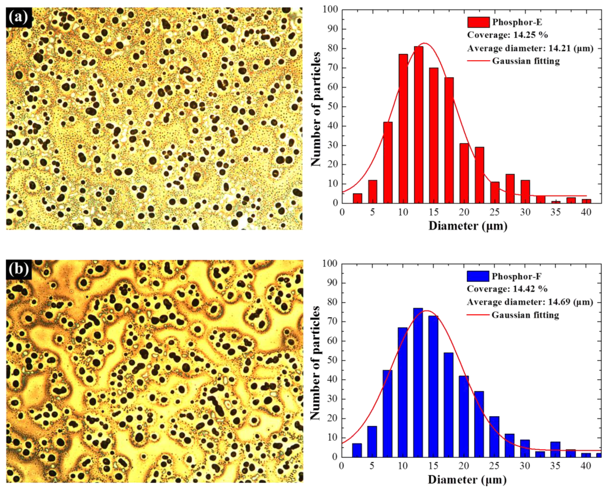
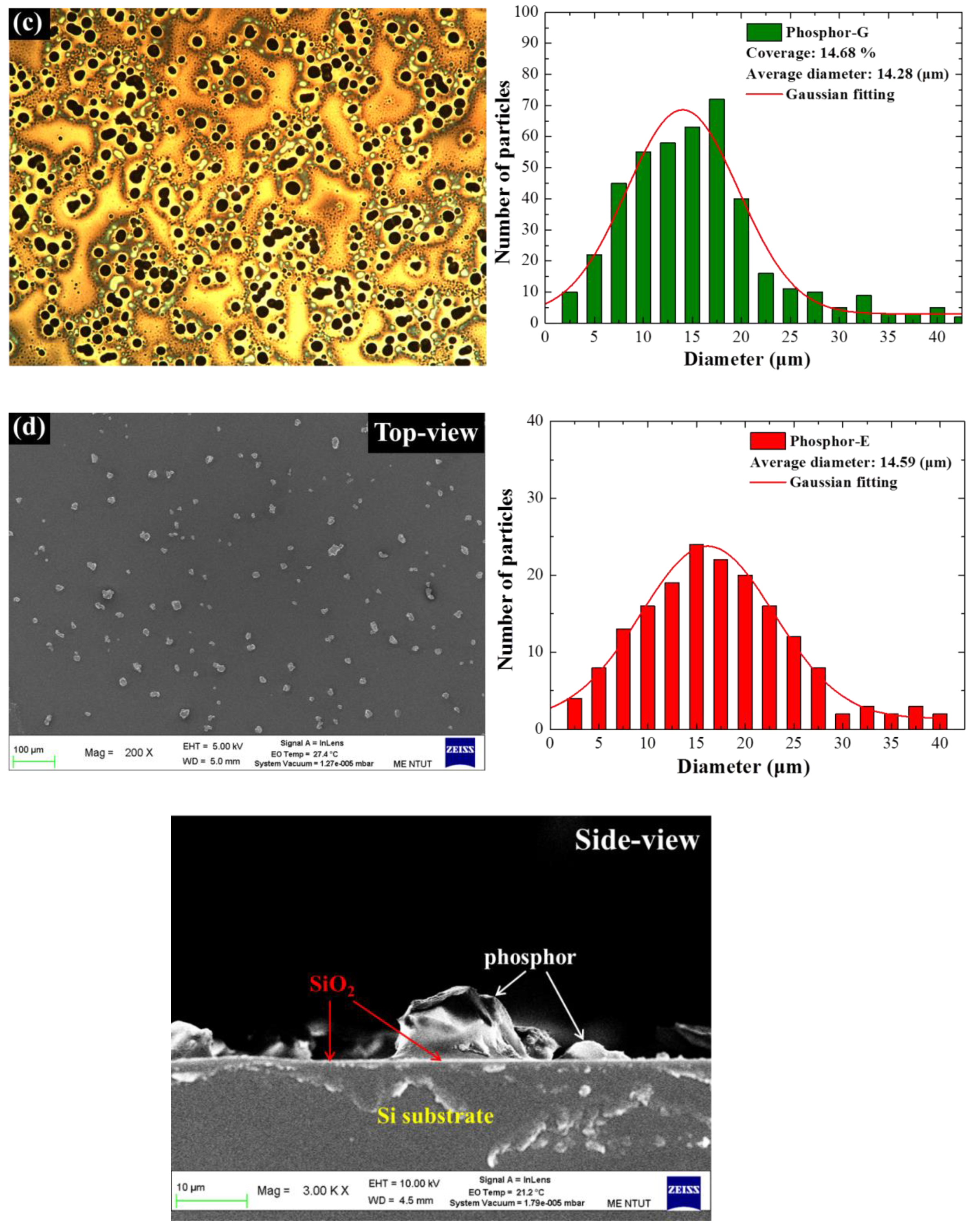
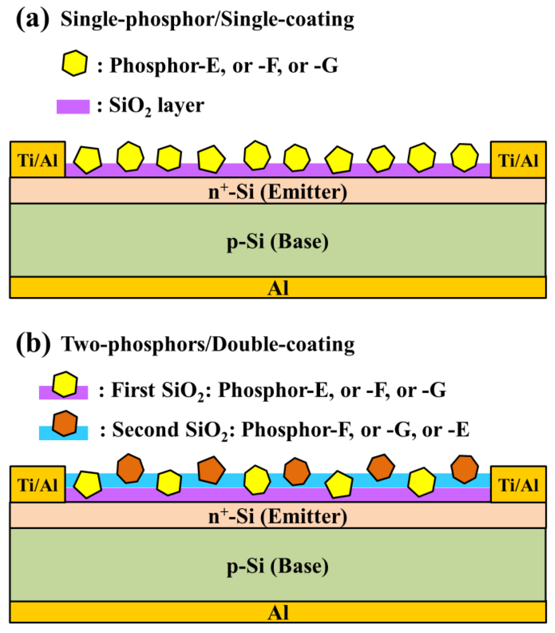
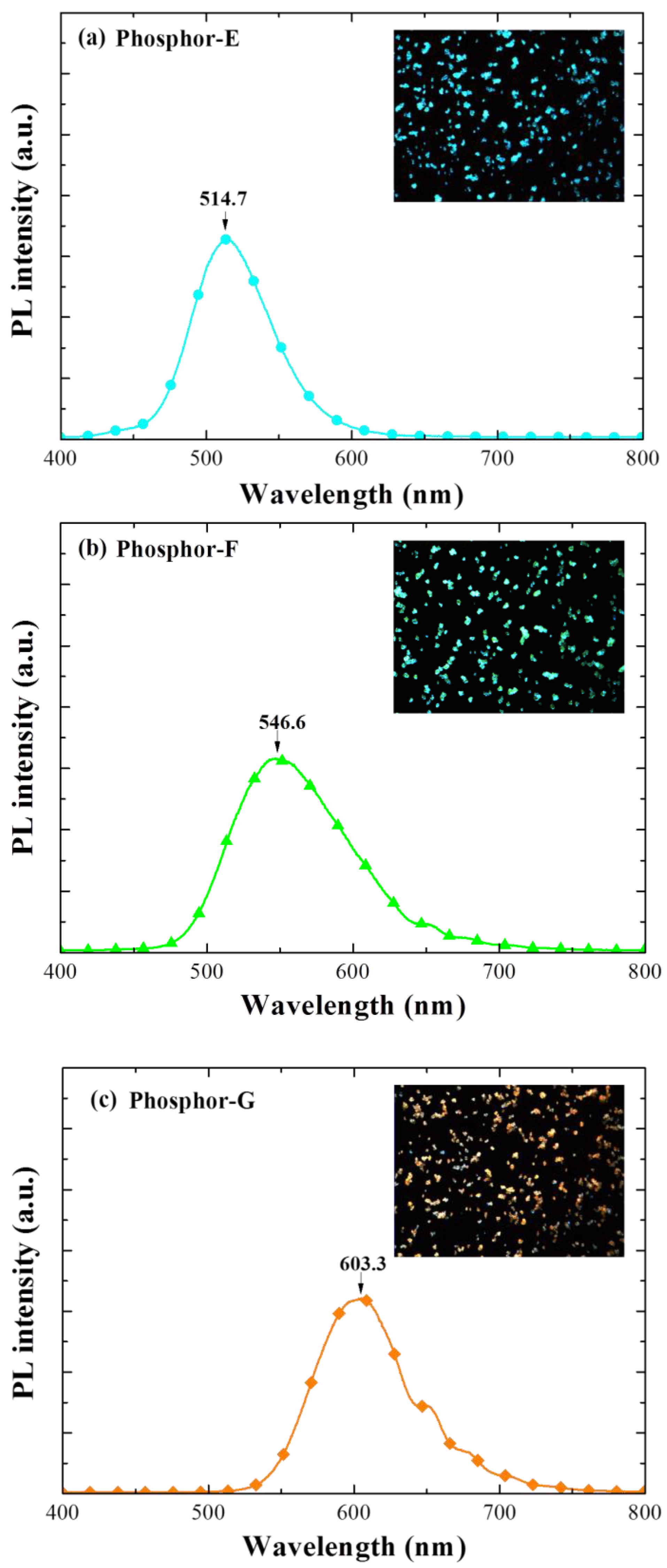
2.1.1. Single Coating with Single Phosphor Particles

In this study, three Eu-doped phosphors (referred to as Phosphor-E, -F, and -G) were assessed in terms of LDS spectral conversion from ultraviolet (UV) to visible (VIS) wavelength bands. The phosphors were obtained from InteMatix (Fremont, CA, USA). Figure 1a presents a schematic diagram showing a silicon substrate (or silicon solar cell) on which was deposited an LDS spectral conversion layer of SiO2 containing a single phosphor. Into a solution containing 1.94 g silicate was mixed 0.06 g (3 wt %) of a single phosphor in powdered form (the particle size from 5 to 20 μm). Then, the LDS layer was created by coating a clean silicon substrate with this solution via spin-on processing at 3500 rpm for 55 s, before being baked at 210 °C for 110 s under an air atmosphere. Note that the mixed solution was applied to the sample drop-wise and held for 5 s prior to spinning.

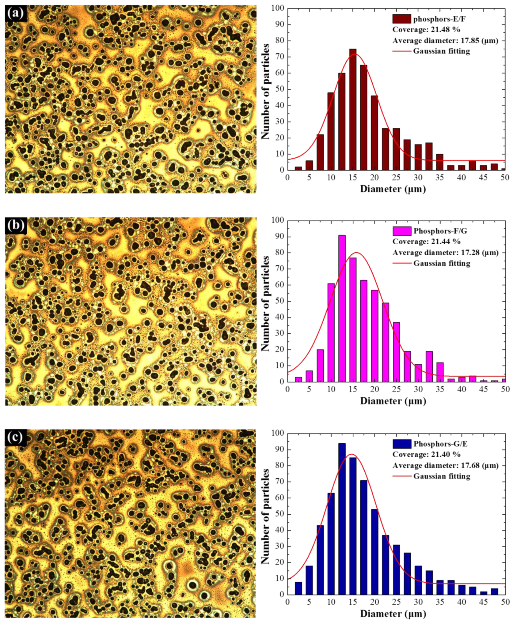
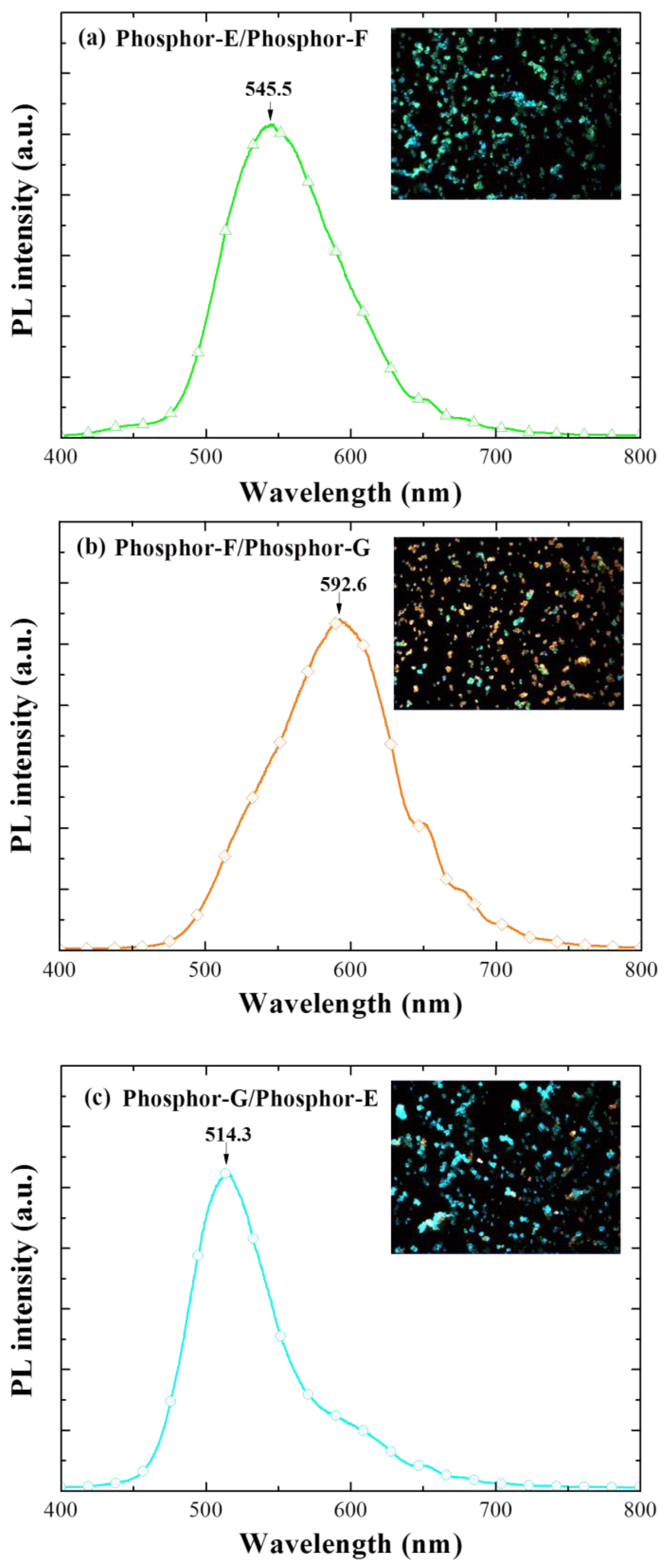
2.1.2. Double-Coatings Using Two Types of Phosphor Particles

As shown in Figure 1b, we fabricated double-layer LDS samples by applying a second SiO2 layer containing a different phosphor over the first layer using the same spin-on coating process. Before applying the second coating, the samples underwent ultrasonic cleaning in acetone and methanol solutions for 5 min followed by rinsing in DI water for 4 min before being dried under ambient N2 for 2 min. Note that in both coating solutions, the concentration of phosphors was 3 wt %. The resulting 1st-layer/2nd-layer configuration is hereafter described according to the constituent phosphor particles: Phosphor-E/-F, Phosphor-F/-G, and Phosphor-G/-E.
The morphology and chemical makeup of samples with a phosphor layer were examined via optical microscopy (OM) and scanning electron microscopy/energy-dispersive spectroscopy (SEM/EDS; Hitachi S-47000, Hitachi High-Tech Fielding Corporation, Tokyo, Japan). The fluorescence emission of the phosphor layer was characterized by obtaining PL measurements at room temperature. The PL (Spex Fluorolog-3, Jobin Yvon Instrument S. A. Inc., Sunnyvale, CA, USA) and optical reflectance spectra were used to reveal the LDS effects of the phosphor layer(s). The reflectance of samples (with and without phosphor particles in the SiO2 layer) was characterized by an UV/VIS/NIR spectrophotometer (PerkinElmer Lambda 35, Waltham, MA, USA).

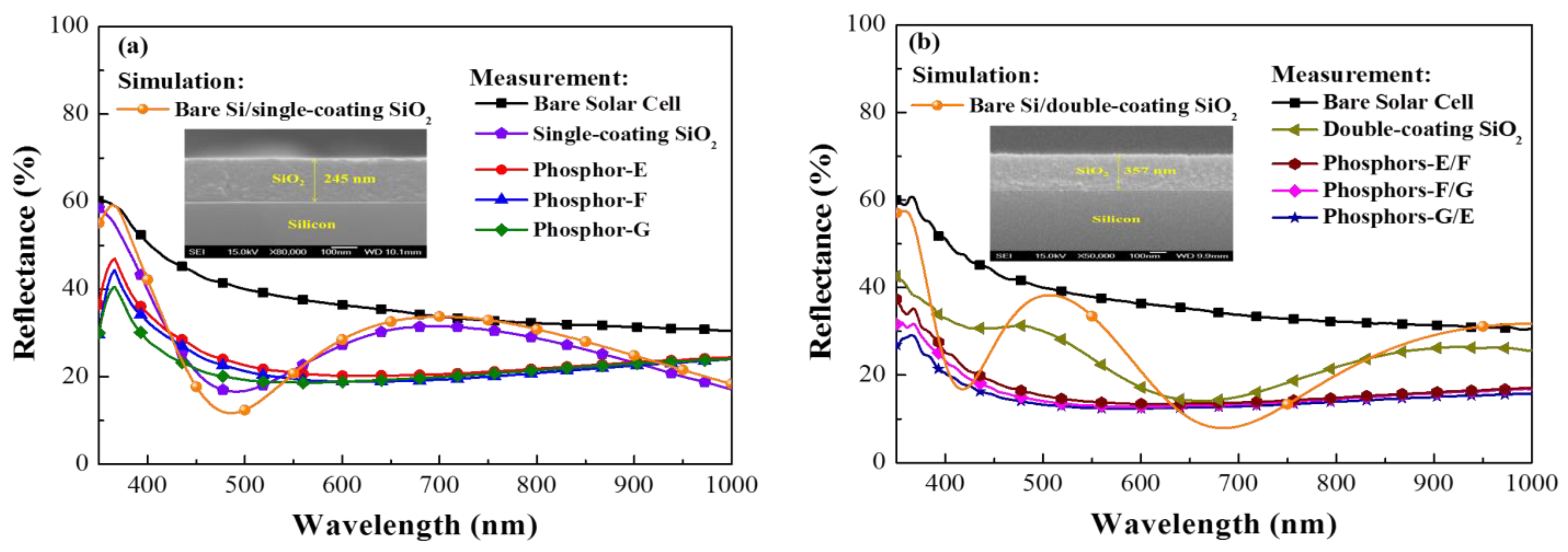
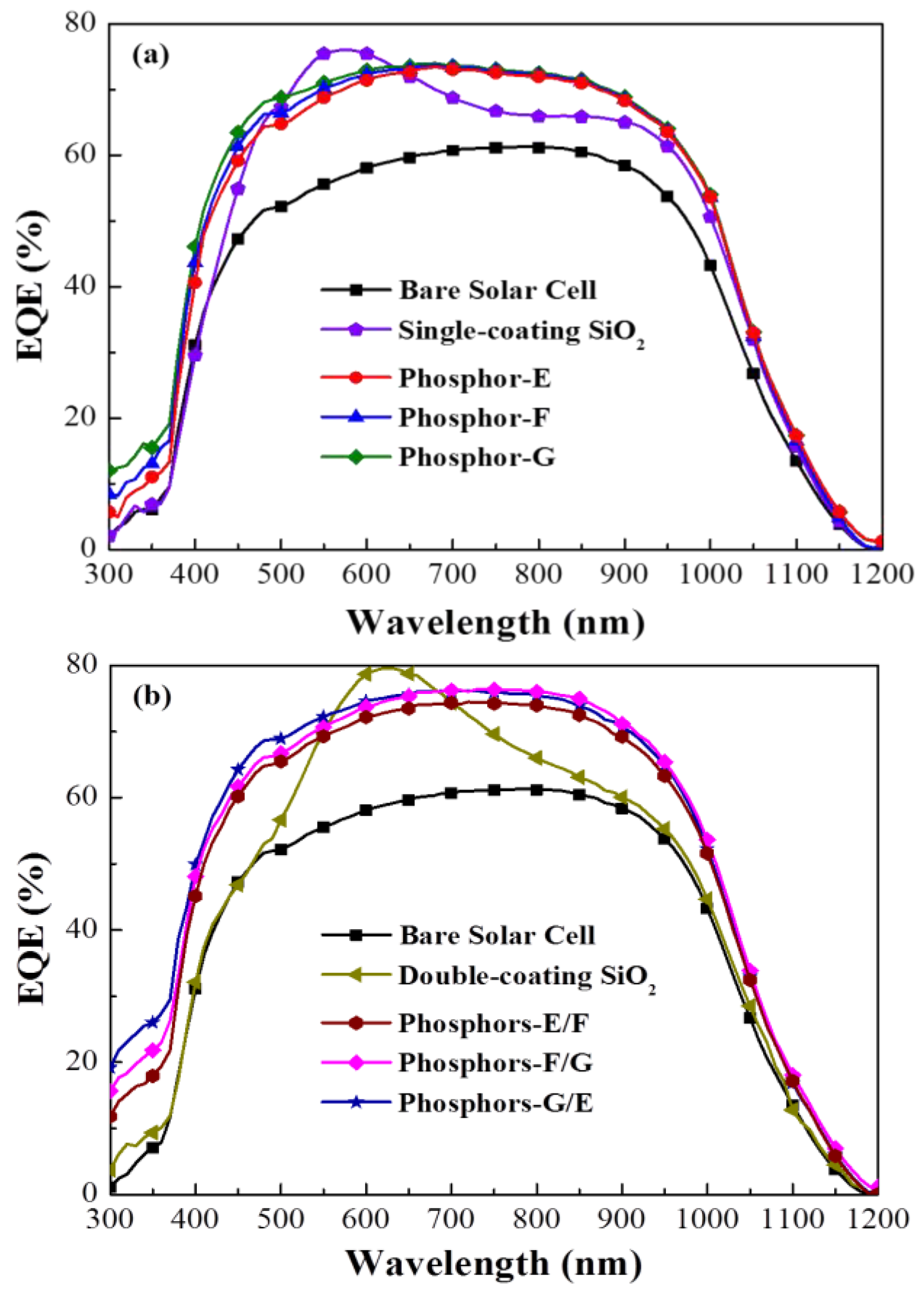
2.2. Characterization of Solar Cells with a Single Layer or Dual Layers of SiO2 Containing Phosphors

The starting material for the solar cell devices was a p-type (100) C-Si wafer (550 μm 10 Ω-cm). The wafer was first cut into samples measuring 1 × 1 cm2, which were then subjected to the standard RCA cleaning process. An n+-Si layer (emitter, 0.35 μm) was created on the front-surface of C-Si via spin processing using a liquid phosphorous source (Phosphorofilm, Emulstione Co., Washington, NJ, USA) followed by heating in a rapid thermal annealing (RTA) chamber at 910 °C for 100 s under ambient N2. The diffused oxide layer remaining on the surface of the Si sample was removed by a BOE solution. Four-point probe measurement showed that the sheet resistance of the n+-Si emitter-layer was roughly 60 Ω/cm2. SIMS profiling revealed that the surface phosphorus concentration was roughly 1.5 × 1020 cm−3. Clean diffused samples underwent isolation, etching to a depth of 0.85 μm via photolithography using an etching solution of HNO3:HF:H2O (1:1:2) for 35 s, which resulted in individual cells measuring 4.1 × 4.1 mm2. A P-electrode and N-electrode were produced as Ohmic contacts by depositing 500 nm-thick Al film on the back side and a Ti (25 nm)/Al (350 nm) on the top surface using e-beam evaporation and a lift-off process. Then, the samples underwent annealing in an RTA chamber under ambient N2 at 445 °C for 23 min to optimize metal/semiconductor contact characteristics, thereby completing the bare-type Si solar cells.
To investigate the effects of LDS on the performance of C-Si solar cells, we coated bare-type C-Si solar cells with a SiO2 layer containing phosphors (Phosphor-E, or -F, or -G) at a concentration of 3 wt % via spin coating (hereafter referred to as single-phosphor/single-coating), as shown in Figure 1a. We assessed broadband LDS effects by applying a second LDS layer over the first layer (hereafter referred to as two-phosphors/double-coating), as shown in Figure 1b. Note that different phosphors were used in the first and second coatings (E/F, F/G, or G/E), but the phosphor concentrations in the two layers were the same (3 wt %). Then, we examined the optical and electrical characteristics of the resulting luminescent down-shifting spectral conversion coatings in terms of optical reflectance, EQE response at wavelengths between 300 and 1000 nm (LSQE-R3015, Enli Technology Co., Kaohsiung, Taiwan), and J–V curves under AM 1.5 G solar simulation. The XES-151S solar simulator (San-Ei Electric Co., Ltd., Osaka, Japan) used in this work was calibrated using a PVM-894 silicon reference cell (PV Measurements Inc., Boulder, CO, USA) certified by the National Renewable Energy Laboratory before tests. All presented data were averaged from three measurements.

3. Results and Discussion

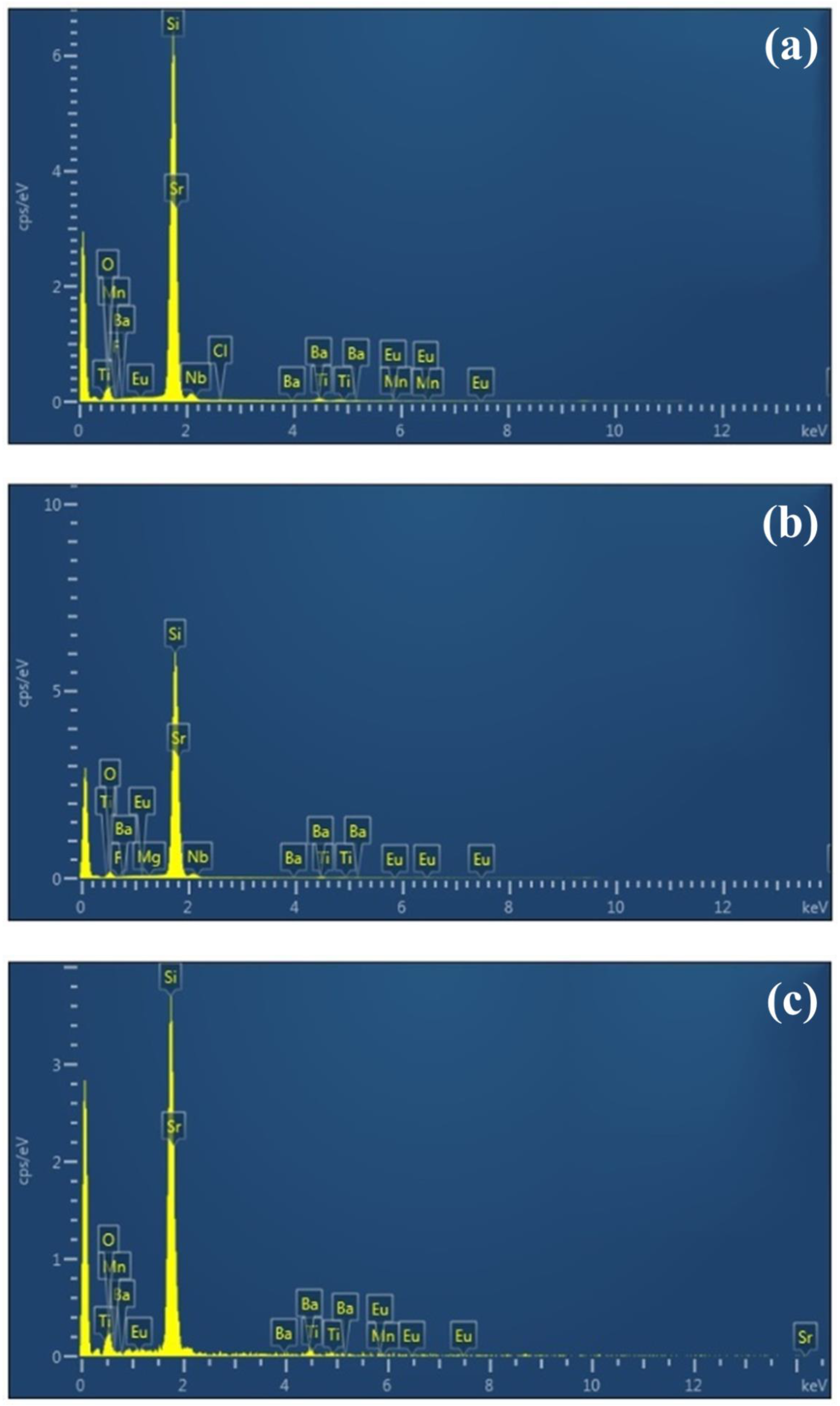
3.1. Characteristics of LDS Layers Containing Phosphors

Figure 2 presents optical images and the particle size distribution of phosphor particles in samples with a single-phosphor SiO2 layer containing (a) Phosphor-E, (b) Phosphor-F, and (c) Phosphor-G. Particle size profiles were derived from the optical images using Image-J software. Due to similarities in the spin-coating coating parameters, the average diameter (14 μm) and surface coverage (14%) of all samples were roughly the same, regardless of the constituent phosphors. Figure 2d presents SEM images (top and side views) of silicon wafers coated with SiO2 and phosphor particles. SEM revealed that the average diameter of the phosphor particles closely matched the OM results (roughly 14 μm). Figure 3 presents the surface morphology and particle-size distribution of samples with two phosphors. The average particle diameter (17 μm) and surface coverage (21%) on the double-coating samples were both higher than on the single-coating samples due to the fact that the empty areas left in the first coating were filled with particles applied during the second coating, and a few particles from the first and second layers overlapped. Figure 2 and Figure 3 present Gaussian fittings to enable a statistical comparison.
Energy-dispersive spectroscopy (EDS) is used in the element analysis of solid samples to characterize the interaction between the X-ray excitation source and sample. Each element within the sample has a unique atomic structure, which produces a unique set of peaks in the EDS spectrum. Figure 4 displays the EDS spectra of SiO2 layers containing different phosphors: (a) Phosphor-E, (b) Phosphor-F, and (c) Phosphor-G. The composition of all phosphor samples was mainly Si, O, Ba, and Sr, with a small quantity of Eu and other elements (F, Ti, Mn, Mg, and Cl). The chemical formulas were as follows: Phosphor-E ([(Sr0.05Ba0.95)0.98Eu0.02]2SiO3.9F0.1), Phosphor-F ([(Sr0.7Ba0.3)0.98Eu0.02]2SiO3.9F0.1), and Phosphor-G ((Sr0.9Ba0.1)3SiO5:Eu), based on information obtained from InteMatix products information.
Figure 5 displays the PL spectra and color optical emission images of samples with a SiO2 layer containing a single phosphor: (a) Phosphor-E, (b) Phosphor-F, and (c) Phosphor-G. The optical images were obtained from samples under blue light illumination. The PL emission peak (λPL) and color were as follows: Phosphor-E (λPL = 514.7 nm and cyan), Phosphor-F (λPL = 546.6 nm and green), Phosphor-G (λPL = 603.3 nm and orange).
Figure 6 displays the PL spectra and color optical emission images of samples with 1st-SiO2 (bottom)/2nd-SiO2 (top) layers comprising various combinations of two phosphors: (a) Phosphor-E/Phosphor-F, or (b) Phosphor-F/Phosphor-G, or (c) Phosphor-G/Phosphor-E. The PL emission-peak and color were as follows: E/F (λPL = 545.5 and green), F/G (λPL = 592.6 nm and orange), and G/E (λPL = 514.3 nm and cyan). Overall, the PL intensity of samples with two phosphors exceeded that of single-phosphor samples (>1.5 times). In addition, the peak PL emission wavelength of dual-phosphor combinations shifted toward the emission wavelength of the 2nd-layer containing Eu-doped phosphor, with a corresponding shift in color toward that of the 2nd layer. Wideband performance was particularly evident in the F/G sample.

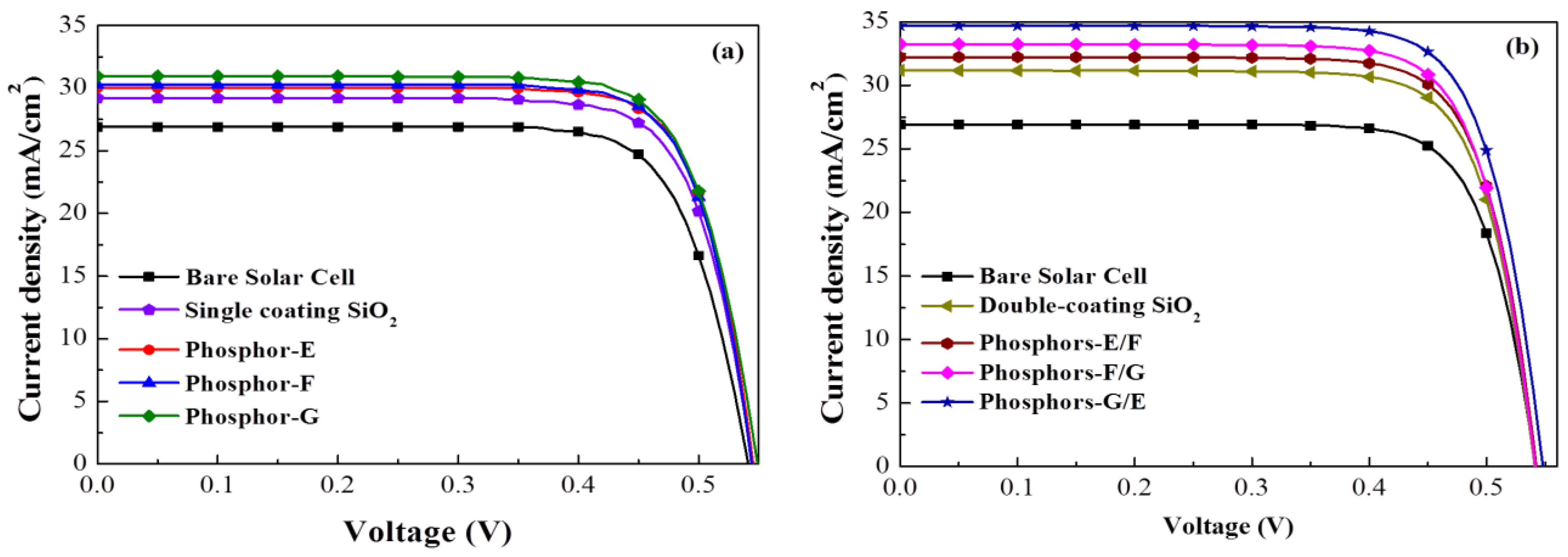
3.2. Performance of Silicon Solar Cells Coated with LDS Layers Comprising One or Two Phosphors

The LDS effect on the efficiency of C-Si solar cells was characterized in terms of optical reflectance, EQE, and J–V characteristics under AM 1.5 G illumination. These values were first obtained from bare cells and cells with a single SiO2 layer for use as a reference. The open-circuit voltage (Voc), short-circuit current-density (Jsc), and conversion efficiency (η) of bare cells were as follows: Voc = 541.3 mV, Jsc = 26.91 mA/cm2, and η = 11.14%. Figure 7a presents the measured reflectance from the three types of solar cells examined in this experiment: bare cells, cells coated with a layer of SiO2, and cells coated with a layer of SiO2 containing phosphors. Figure 7a also shows the simulated reflectance of bare Si/SiO2. Note that the SiO2 layer was created using a single spin-coating operation using silicate solution. In simulations using TFCalcTM simulation software, the thickness of the SiO2 layer was estimated at 245 nm; however, the measured thickness of SiO2 in actual samples was roughly 240 nm, as confirmed in side-view SEM images (inset in Figure 7a). The reflectance of the cell with a SiO2 layer was lower than that of the bare cell across the entire range of wavelengths, which was due to the anti-reflective effects of the SiO2 film. The reflectance of cells with phosphor particles was even lower than that of cells with only a SiO2 layer over a wavelength range of 350 to 410 nm (owing to the absorption of incident light by the phosphors) and 550 to 900 nm (owing to the forward scattering of incident photons). Figure 7b presents the measured reflectance and simulated reflectance of cells with double-coatings. In simulations, the thickness of samples with a double coating of SiO2 was roughly 350 nm; however, the thickness of actual samples was 357 nm, as confirmed in side-view SEM images (inset in Figure 7b). The overall reflectance of samples with a double-coating of SiO2 was lower than that of samples with a single-coating, and the wavelength corresponding to the lowest reflectance was red-shifted from 500 to 700 nm. The reflectance values of cells with a double coating of SiO2 containing phosphors was lower than the single layer equivalents over a limited wavelength range (350 to 410 nm) as well as samples with a double-coating of SiO2 over the full wavelength range (350–1000 nm). The G-/E-phosphor combination presented the lowest overall reflectance. As shown in Table 1, the average weighted reflectance (RW) was derived for two wavelength ranges (350–450 nm and 350–1000 nm). RW values were used to characterize the LDS effects induced by phosphors (single-phosphor and two-phosphor). Based on the reflectance results, we expected that samples with a double coating of SiO2 containing two different phosphors would present the highest EQE response.
Figure 8a displays the EQE spectra of a bare cell, a cell coated with a layer of SiO2, and cells coated with a layer of SiO2 containing various phosphors. The EQE of cells with a double coating of SiO2 containing phosphors was higher than that of the cell with only SiO2, except over a wavelength range of 460 to 630 nm, owing to LDS effects and forward scattering caused by the phosphors. The EQE of the sample with Phosphor-G was higher than that of the samples with Phosphor-F or Phosphor-E over a wavelength range of 350 to 450 nm. As shown in Table 1, we calculated the average external quantum efficiency (EQEW) for wavelength ranges of 350–450 nm and 350–1000 nm. The EQE results are in good agreement with those of optical reflectance and PL results, due to the fact that the photons emitted by Phosphor-G and Phosphor-F fall within the range of wavelengths to which Si devices are highly responsive. Figure 8b presents the EQE spectra of the cell with two phosphors. The overall EQE value of double-coated samples exceeded that of single-coated samples, and the wavelength corresponding to the highest EQE was red shifted from 550 to 630 nm. Similarly, the EQE values of the cells with two phosphors exceeded those of cells with a single coating over a wavelength range of 350 to 410 nm. The highest EQE was obtained from the G/E sample. Table 1 also lists the EQEW of the double-layer cells. We expected that samples with a double coating of SiO2 containing two phosphors (G/E configuration) would present the highest photovoltaic performance. Table 1 lists the integrated Jsc values from the EQE spectra to enable a comparison of LDS and anti-reflection effects. To further clarify the relationship, we calculated the EQEW as follows:
E Q E W = 350 n m 1000 n m E Q E ( λ ) ϕ ( λ ) d λ 350 n m 1000 n m ϕ ( λ ) d λ × 100 %
where EQE(λ) is the EQE at a given λ (wavelength), and ϕ(λ) is the photon flux of AM 1.5 G at that λ.
Figure 9a presents the J–V curves of a bare cell, a cell with a layer of SiO2, and cells with a layer of SiO2 containing Eu-doped phosphors obtained under AM 1.5 G solar simulation. The Voc (544.8 mV), Jsc (29.2 mA/cm2), and η (12.28%) of the cell coated with a SiO2 layer exceeded those of the bare cell (541.3 mV, 26.91 mA/cm2, 11.14%), owing to the passivation and anti-reflection effects of the SiO2 layer. The Jsc (30.04–30.97 mA/cm2) and η (12.82–13.07%) of the cells with a single phosphor were higher than those of the cell with only SiO2, owing to LDS effects and forward scattering. The cell with Phosphor-G presented Jsc (30.97 mA/cm2) and η (13.07%) values that were significantly higher than those of the cell with Phosphor-F (30.26 mA/cm2, 12.93%) or Phosphor-E (30.04 mA/cm2, 12.82%). Table 2 lists the conversion efficiency enhancement (ΔηDS) of cells with an LDS layer (SiO2: phosphors, one-phosphor), compared to the cell with a single coating of pure SiO2. Figure 9b presents the photovoltaic J–V curves of cells with two-phosphor combinations. The Jsc and η values of dual-phosphor dual-coating samples exceeded those of their single-phosphor single-coating counterparts. The Jsc enhancement of dual-layer phosphor cells (ΔJsc = 19.81–28.91%) and η (Δη = 22.03–31.63%) exceeded those of their single-layer counterparts (ΔJsc = 11.63–15.09% and Δη = 15.16–17.39%), which was comparable to those of the bare reference cell. The Phosphor-G/E combination achieved the highest Jsc and η values overall. Table 2 lists the ΔηDS of dual-phosphor dual-coating samples compared to the cell with double-coating of pure SiO2 layers. Table 2 also summarizes the photovoltaic performance of all evaluated cells.

4. Conclusions

This study examined the optical and electrical effects of a luminescent down-shifting (LDS) layer containing a single species or two species of Eu-doped phosphors applied via spin coating. PL, optical reflectance, and EQE measurements revealed the LDS effects of the phosphors. The highest conversion efficiency (13.07%) was obtained in solar cells with Phosphor-G, which was due to the high responsivity of the silicon to LDS photons. The combination of two phosphors had more pronounced effects on broadband LDS emissions than did the single coatings containing a single phosphor. The solar cell with a Phosphor-G/Phosphor-E combination yielded the highest short-circuit current density (34.69 mA/cm2) and conversion efficiency (14.66%) corresponding to a 31.63% improvement over that of bare Si solar cells.

Author Contributions

All authors conceived the experiments and results; W.-J.H. designed, analyzed, and wrote the first draft of the paper; J.-J.L. performed the experiments and analyzed data. B.-X.K. conducted EQE and J-V measurements. All authors have read and agreed to the published version of the manuscript.

Funding

The Ministry of Science and Technology of the Republic of China under Grant MOST 109-2221-E-027-117-MY2.

Institutional Review Board Statement

Not applicable.

Informed Consent Statement

Not applicable.

Data Availability Statement

Not applicable.

Conflicts of Interest

The authors declare no conflict of interest.

References

  1. Tryyestad, C.; Sharma, N.; Rolser, O.; Smeets, B.; van de Staaij, J.; Gruenewald, T. Global Energy Perspective 2021: Reference case, Energy Insights by McKinsey & Company. January 2021. Available online: https://www.mckinsey.com/industries/oil-and-gas/our-insights/global-energy-perspective-2021 (accessed on 1 January 2021).
  2. Kober, T.; Schiffer, H.-W.; Densing, M.; Panos, E. Global energy perspectives to 2060—WEC’s world energy scenarios 2019. Energy Strateg. Rev. 2020, 31, 100523. [Google Scholar] [CrossRef]
  3. IRENA. Global Renewables Outlook: Energy Transformation 2050; International Renewable Energy Agency: Abu Dhabi, United Arab Emirates, 2020. [Google Scholar]
  4. IRENA. Future of Solar Photovoltaic: Deployment, Investment, Technology, Grid Integration and Socio-Economic, Aspects (A Global Energy Transformation: Paper); International Renewable Energy Agency: Abu Dhabi, United Arab Emirates, 2019; Available online: https://irena.org/-/media/Files/IRENA/Agency/Publication/2019/Nov/IRENA_Future_of_Solar_PV_2019.pdf (accessed on 1 November 2019).
  5. Gielen, D.; Boshell, F.; Saygin, D.; Bazilian, M.D.; Wagner, N.; Gorini, R. The role of renewable energy in the global energy transformation. Energy Strateg. Rev. 2019, 24, 38–50. [Google Scholar] [CrossRef]
  6. Hirst, L.C. 1.14 Principles of Solar Energy Conversion. Compr. Renew. Energy 2012, 1, 293–313. [Google Scholar] [CrossRef]
  7. Battaglia, C.; Cuevas, A.; Wolf, S.D. High-efficiency crystalline silicon solar cells: Status and perspectives. Energy Environ. Sci. 2016, 9, 1552–1576. [Google Scholar] [CrossRef] [Green Version]
  8. Roosloot, N.; Neder, V.; Haug, H.; You, C.C.; Polman, A.; Marstein, E.S. Broadband angular color stability of dielectric thin film-coated pyramidal textured Si for photovoltaics. J. Appl. Phys. 2021, 129, 173104. [Google Scholar] [CrossRef]
  9. Kale, A.S.; Nemeth, W.; Guthrey, H.; Page, M.; Al-Jassim, M.; Young, D.L.; Agarwal, S.; Stradins, P. Modifications of textured silicon surface morphology and its effect on poly-Si/SiOx contact passivation for silicon solar cells. IEEE J. Photovolt. 2019, 9, 1513–1521. [Google Scholar] [CrossRef]
  10. Shanmugam, N.; Pugazhendhi, R.; Elavarasan, R.M.; Kasiviswanathan, P.; Das, N. Anti-reflective coating materials: A holistic review from PV perspective. Energies 2020, 13, 2631. [Google Scholar] [CrossRef]
  11. Sagar, R.; Rao, A. Nanoscale TiO2 and Ta2O5 as efficient antireflection coatings on commercial monocrystalline silicon solar cell. J. Alloys Compd. 2021, 862, 158464. [Google Scholar] [CrossRef]
  12. Meyer, F.; Savoy, A.; Leon, J.J.D.; Persoz, M.; Niquille, X.; Allebé, C.; Nicolay, S.; Haug, F.-J.; Ingenito, A.; Ballif, C. Optimization of front SiNx/ITO stacks for high-efficiency two-side contacted c-Si solar cells with co-annealed front and rear passivating contacts. Sol. Energy Mater. Sol. Cells 2021, 219, 110815. [Google Scholar] [CrossRef]
  13. Hirst, L.C.; Ekins-Daukes, N.J. Fundamental losses in solar cells. Prog. Photovolt Res. Appl. 2011, 19, 286–293. [Google Scholar] [CrossRef]
  14. Tiedje, T.; Yablonovitch, E.; Cody, G.D.; Brooks, B.G. Limiting efficiency of silicon solar cells. IEEE Trans. Electron. Devices 1984, ED-31, 711–716. [Google Scholar] [CrossRef]
  15. Richter, A.; Hermle, M.; Glunz, S.W. Reassessment of the limiting efficiency for crystalline silicon solar cells. IEEE J. Photovolt. 2013, 3, 1184–1191. [Google Scholar] [CrossRef]
  16. Klampaftis, E.; Richards, B.S. Improvement in multi-crystalline silicon solar cell efficiency via addition of luminescent material to EVA encapsulation layer. Prog. Photovolt. Res. Appl. 2011, 19, 345–351. [Google Scholar] [CrossRef]
  17. Chander, N.; Sardana, S.K.; Parashar, P.K.; Khan, A.F.; Chawla, S.; Komarala, V.K. Improving the short-wavelength spectral response of silicon solar cells by spray deposition of YVO4:Eu3+ downshifting phosphor nanoparticles. IEEE J. Photovolt. 2015, 5, 1373–1379. [Google Scholar] [CrossRef]
  18. Day, J.; Senthilarasu, S.; Mallick, T.K. Improving spectral modification for applications in solar cells: A review. Renew. Energy 2019, 132, 186–205. [Google Scholar] [CrossRef]
  19. Liu, S.-M.; Chen, W.; Wang, Z.-G. Luminescence Nanocrystals for Solar Cell Enhancement. J. Nanosci. Nanotechnol. 2010, 10, 1418–1429. [Google Scholar] [CrossRef] [PubMed]
  20. Romero-Romo, W.; Carmona-Téllez, S.; Lozada-Morales, R.; Soriano-Romero, O.; Caldiño, U.; Álvarez-Ramos, M.E.; Zayas, M.E.; Meza-Rocha, A.N. Down-shifting and down-conversion emission properties of novel CdO-P2O5 invert glasses activated with Pr3+ and Pr3+/Yb3+ for photonic applications. Opt. Mater. 2021, 116, 111009. [Google Scholar] [CrossRef]
  21. Chang, W.; Li, L.; Dou, M.; Yan, Y.; Jiang, S.; Pan, Y.; Cui, M.; Wu, Z.; Zhou, X. Dual-mode downconversion luminescence with broad near-ultraviolet and blue light excitation in Tm3+/Yb3+ codoped oxy-fluoride glasses for c-Si solar cells. Mater. Res. Bull. 2019, 112, 109–114. [Google Scholar] [CrossRef]
  22. Yadav, R.V.; Yadav, R.S.; Bahadur, A.; Rai, S.B. Down shifting and quantum cutting from Eu3+, Yb3+ co-doped Ca12Al14O33 phosphor: A dual mode emitting material. RSC Adv. 2016, 6, 9049–9056. [Google Scholar] [CrossRef]
  23. Jia, Y.; Poncé, S.; Miglio, A.; Mikami, M.; Gonze, X. Design rule for the emission linewidth of Eu2+-activated phosphors. J. Lumines. 2020, 224, 117258. [Google Scholar] [CrossRef]
  24. Shao, G.; Lou, C.; Xiao, D. Enhancing the efficiency of solar cells by down shifting YAG: Ce3+ phosphors. J. Lumines. 2015, 157, 344–348. [Google Scholar] [CrossRef]
  25. Klampaftis, E.; Ross, D.; McIntosh, K.R.; Richards, B.S. Enhancing the performance of solar cells via luminescent down-shifting of the incident spectrum: A review. Sol. Energy Mater. Sol. Cells 2009, 93, 1182–1194. [Google Scholar] [CrossRef]
  26. AL-Shomar, S.M. Synthesis and characterization of Eu3+ doped TiO2 thin films deposited by spray pyrolysis technique for photocatalytic application. Sol. Energy Mater. Res. Express 2021, 8, 026402. [Google Scholar] [CrossRef]
  27. Yang, X.; Chen, J.; Zheng, S.; Chen, C. A downshifting Eu3+ doped glass embedded with concave pyramid microstructure to improve the efficiency of silicon solar cell. J. Rare Earths 2020, 38, 1158–1164. [Google Scholar] [CrossRef]
  28. Fix, T.; Nonat, A.; Imbert, D.; Pietro, S.D.; Mazzanti, M.; Slaoui, A.; Charbonnière, L.J. Enhancement of silicon solar cells by downshifting with Eu and Tb coordination complexes. Prog. Photovolt. Res. Appl. 2016, 24, 1251–1260. [Google Scholar] [CrossRef]
  29. Ho, W.-J.; Shen, Y.-T.; Liu, J.-J.; You, B.-J.; Ho, C.-H. Enhancing photovoltaic performance using broadband luminescent down-shifting by combining multiple species of Eu-doped silicate phosphors. Nanomaterials 2017, 7, 340. [Google Scholar] [CrossRef] [PubMed]
  30. Benharrat, L.; Guerbous, L.; Bradai, D.; Boukerika, A.; Manseri, A.; Selmi, N.; Rahal, B.; Hamroun, M.S.E. Preparation and characterization of luminescent YPO4: Eu3+ thin films using sol gel spin coating method. Thin Solid Film. 2020, 694, 137738. [Google Scholar] [CrossRef]
  31. Ho, W.-J.; Shen, Y.-T.; Deng, Y.-J.; Yeh, C.-W.; Sue, R.-S. Performance enhancement of planar silicon solar cells through utilization of two luminescent down-shifting Eu-doped phosphor species. Thin Solid Film. 2016, 618, 141–145. [Google Scholar] [CrossRef]
  32. Ho, W.-J.; You, B.-J.; Liu, J.-J.; Bai, W.-B.; Syu, H.-J.; Lin, C.-F. Photovoltaic performance enhancement of silicon solar cells based on combined ratios of three species of europium-doped phosphors. Materials 2018, 11, 845. [Google Scholar] [CrossRef] [PubMed] [Green Version]
  33. Lu, P.-C.; Ho, W.-J.; Liu, J.-J.; Yu-Ren Chen, Y.-R.; Chien, Y.-C.; Chiu, W.-C. External quantum efficiency response and conversion efficiency enhancement of silicon solar cells based on multiple layers of up conversion phosphors coating. In Proceedings of the Opto-Electronics and Communications Conference (OECC) 2020, Taipei, Taiwan, 4–8 October 2020. [Google Scholar] [CrossRef]
Figure 1. Schematic diagram of the sample with (a) single coating of SiO2 containing a single phosphor, and (b) a double coating of SiO2 containing two different phosphors.
Materials 15 00452 g001
Figure 2. Optical images and particle-size distributions of single-phosphor samples: (a) Phosphor-E, (b) Phosphor-F, and (c) Phosphor-G; (d) SEM images (top and side views) of the silicon wafer coated with SiO2 and phosphor particles.
Materials 15 00452 g002aMaterials 15 00452 g002b
Figure 3. Optical images and particle-size distribution of samples with dual-coatings of phosphors: (a) E/F; (b) F/G; and (c) G/E.
Materials 15 00452 g003
Figure 4. EDS spectra of silicon substrates deposited a SiO2 layer containing a single phosphor: (a) Phosphor-E; (b) Phosphor-F; and (c) Phosphor-G.
Materials 15 00452 g004
Figure 5. PL spectra and color optical emission images, for the samples with a SiO2 layer containing single phosphors: (a) Phosphor-E, (b) Phosphor-F, and (c) Phosphor-G.
Materials 15 00452 g005
Figure 6. PL spectra of samples with bottom/top LDS layers containing two phosphors: (a) E/F; (b) F/G; (c) G/E.
Materials 15 00452 g006
Figure 7. Measured and simulated reflectance of all cells in this study: (a) single-coating with single phosphor; (b) double-coating with two phosphors.
Materials 15 00452 g007
Figure 8. EQE spectra of proposed silicon solar cells: (a) single coating; (b) double coating.
Materials 15 00452 g008
Figure 9. J–V curves of silicon solar cells: (a) single coating; (b) double coating, under AM 1.5 G simulation.
Materials 15 00452 g009
Table 1. Average weighted reflectance (RW) and average weighted external quantum efficiency (EQEW) calculated for wavelength ranges of 350–450 nm and 350–1000 nm. Integrated Jsc values calculated from EQE spectra (350–1000 nm).
SampleRW (%)
@ 350–450 nm
RW (%)
@ 350–1000 nm
EQEW (%)
@ 350–450 nm
EQEW (%)
@ 350–1000 nm
Cal. Jsc
(mA/cm2)
Bare solar cell49.8437.3532.2052.9322.29
Single-coating SiO236.1826.7433.8662.4726.19
SiO2: Phosphor-E33.4823.4341.6864.3027.04
SiO2: Phosphor-F31.2722.1443.9965.2627.29
SiO2: Phosphor-G27.7821.4546.4066.2127.66
Double-coating SiO233.4523.6235.9664.0826.54
Phosphor-E/Phosphor-F24.8016.1645.3965.5927.73
Phosphor-F/Phosphor-G22.4715.3147.7467.4428.28
Phosphor-G/Phosphor-E20.1114.4250.3468.1728.67
Table 2. Photovoltaic performance of bare cell, cell with SiO2 layer, and cells with phosphors.
SampleVoc
(mV)
Jsc
(mA/cm2)
FF
(%)
η
(%)
ΔJsc
(%)
Δη
(%)
ΔηDS
(%)
Bare solar (SC)541.326.9176.4511.14------
Single-coating SiO2544.829.2077.2212.288.5110.31--
SiO2: Phosphor-E546.830.0478.0712.8211.6315.164.40
SiO2: Phosphor-F547.130.2678.0812.9312.4516.085.29
SiO2: Phosphor-G548.130.9777.0113.0715.0917.396.43
Double-coating SiO2542.631.1877.2213.0615.8717.32--
Phosphor-E/Phosphor-F543.432.2477.5713.5919.8122.034.06
Phosphor-F/Phosphor-G544.433.2577.2813.9923.5625.627.12
Phosphor-G/Phosphor-E547.434.6977.1914.6628.9131.6312.25
Publisher’s Note: MDPI stays neutral with regard to jurisdictional claims in published maps and institutional affiliations.

