
OFF-State Leakage Suppression in Vertical Electron–Hole Bilayer TFET Using Dual-Metal Left-Gate and N+-Pocket


Abstract
1. Introduction
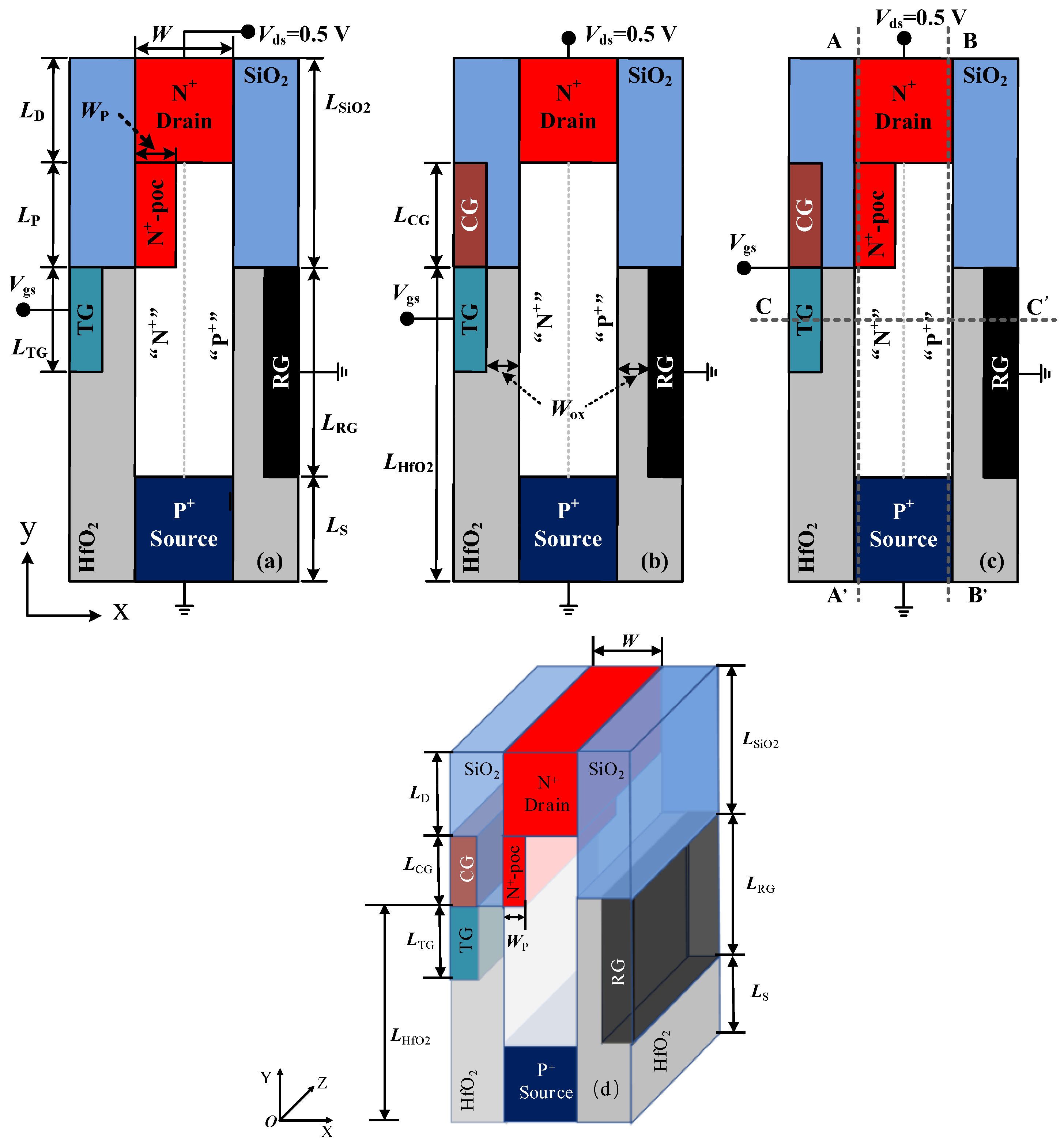
2. Devices Structure and Simulation Methods
3. Results and Discussion
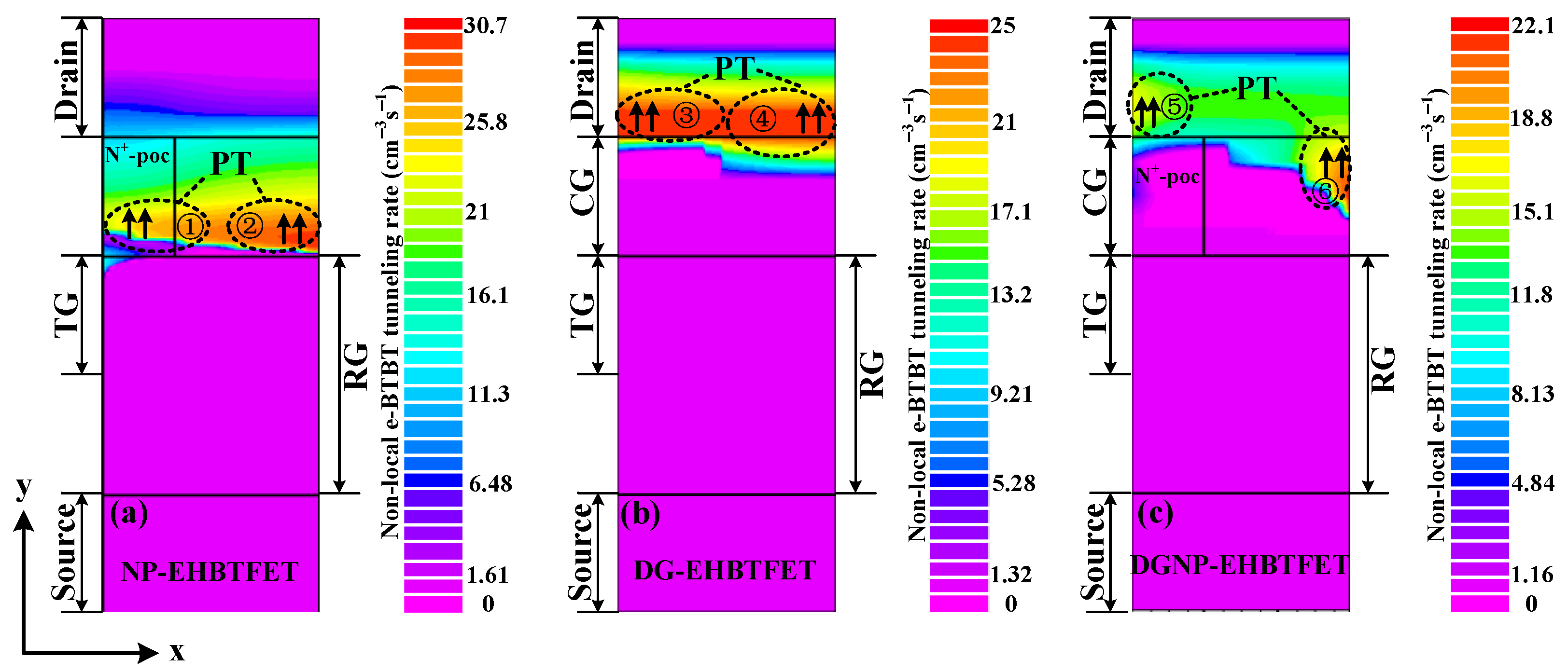
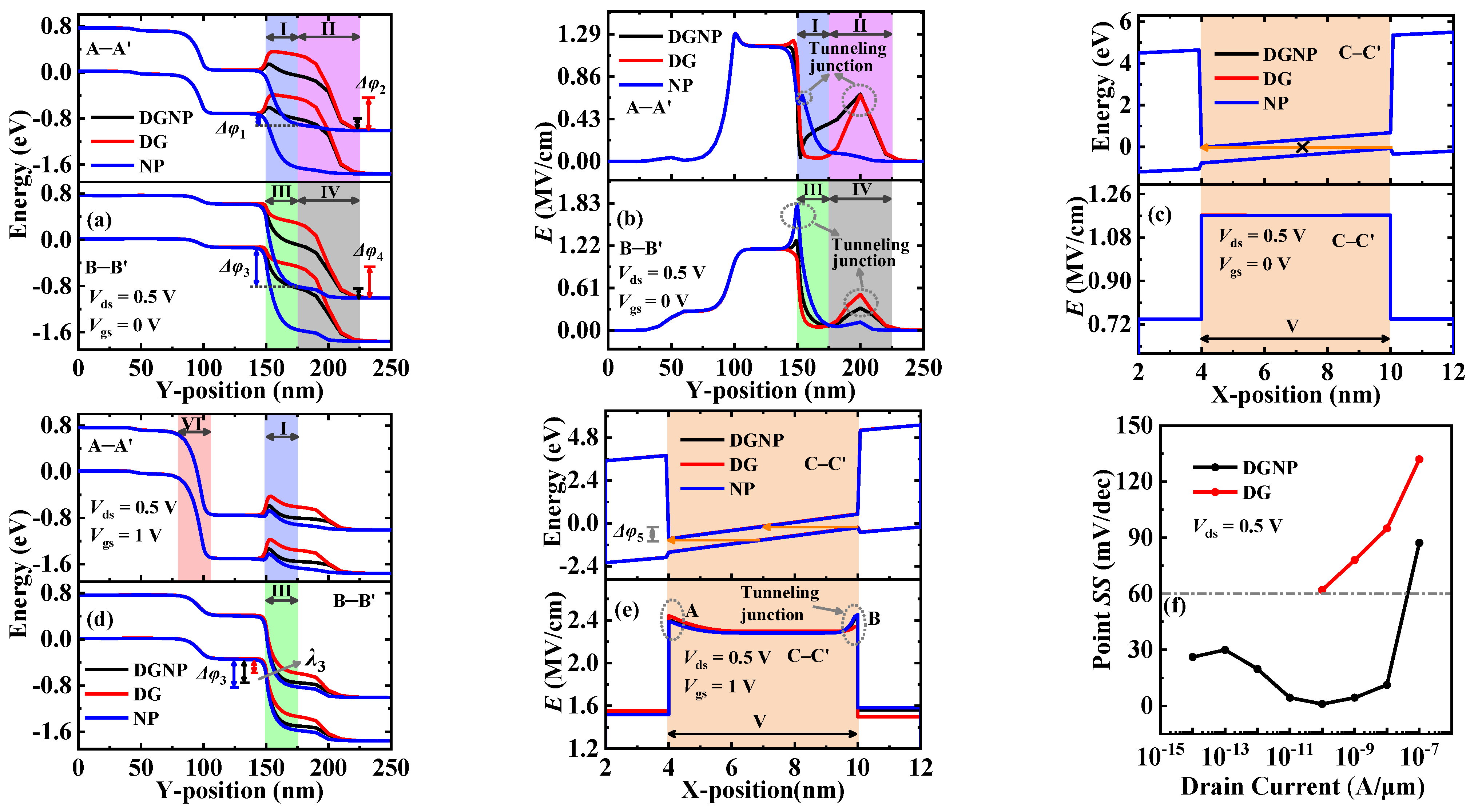
3.1. Operating Mechanism of Three EHBTFETs
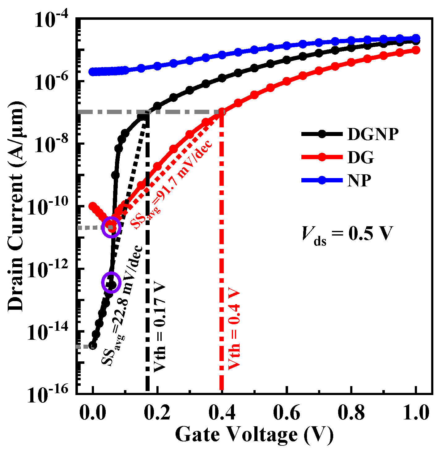
3.2. Comparison of DC Performance among Three EHBTFETs
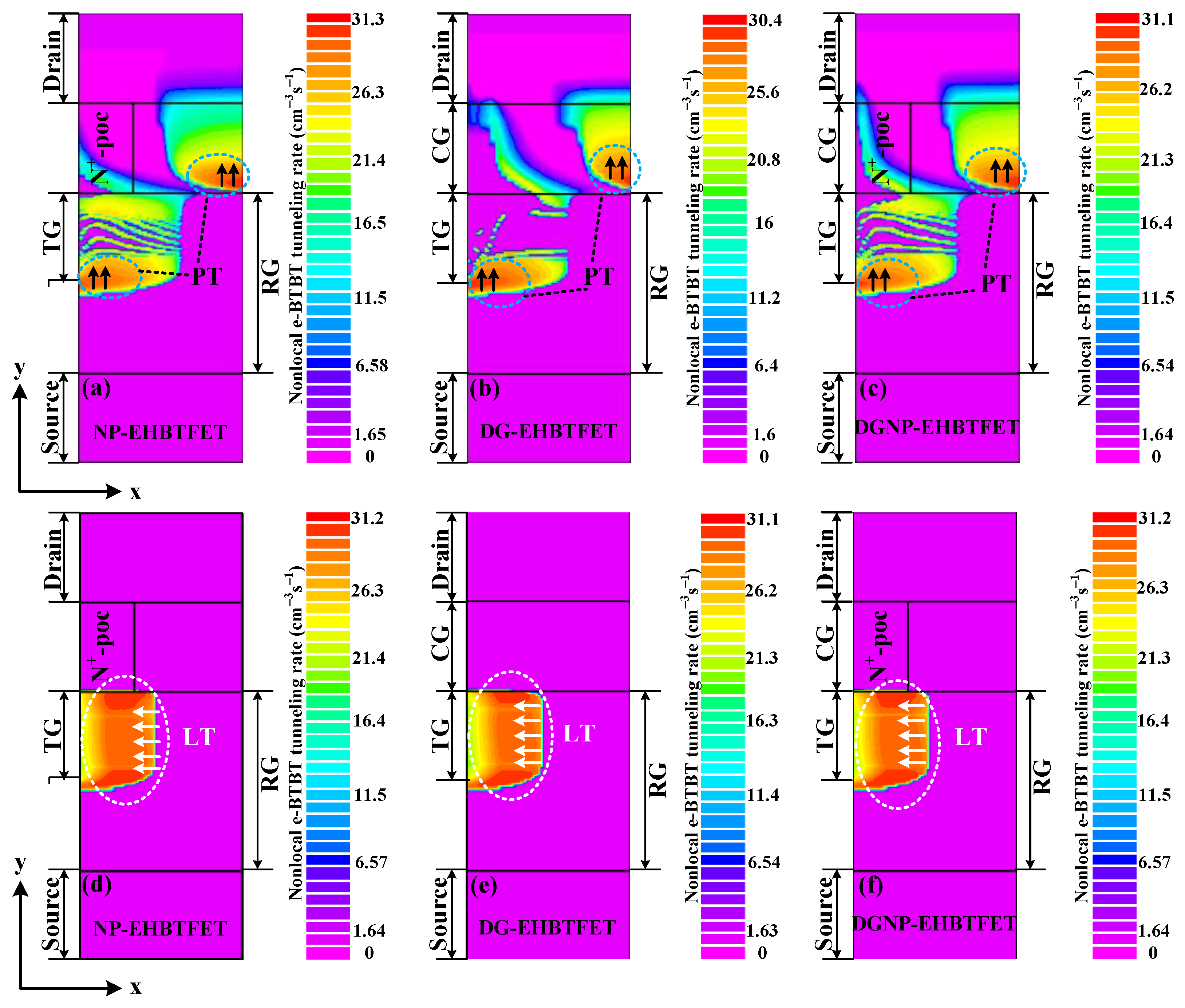
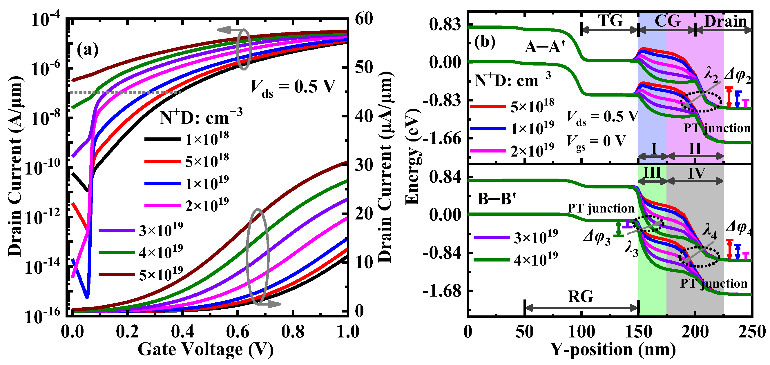
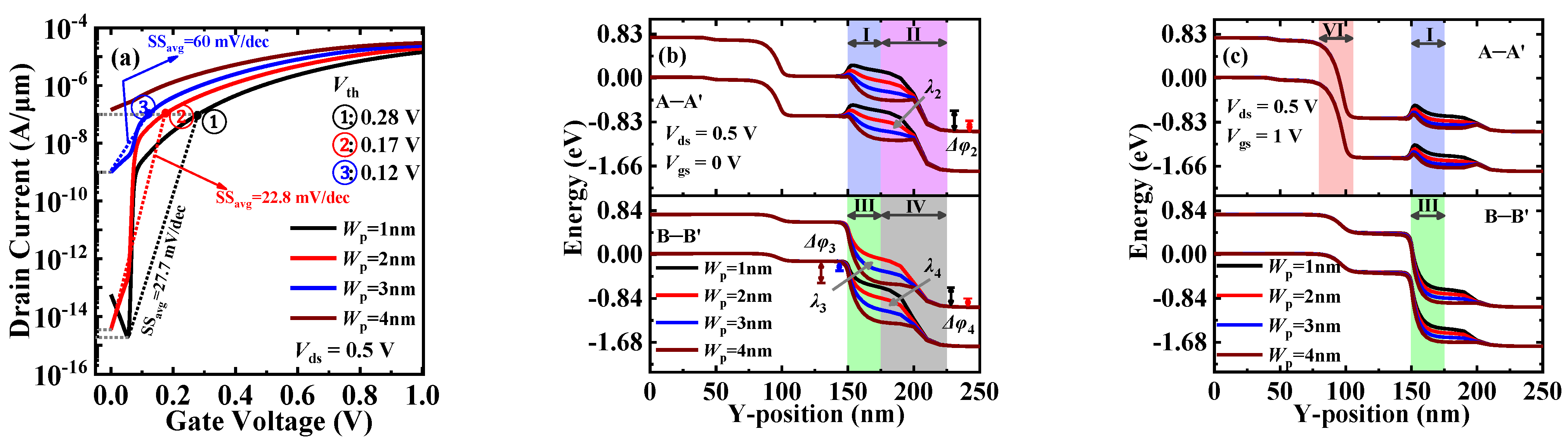
3.3. Effect of N+-Pocket on DGNP-EHBTFET
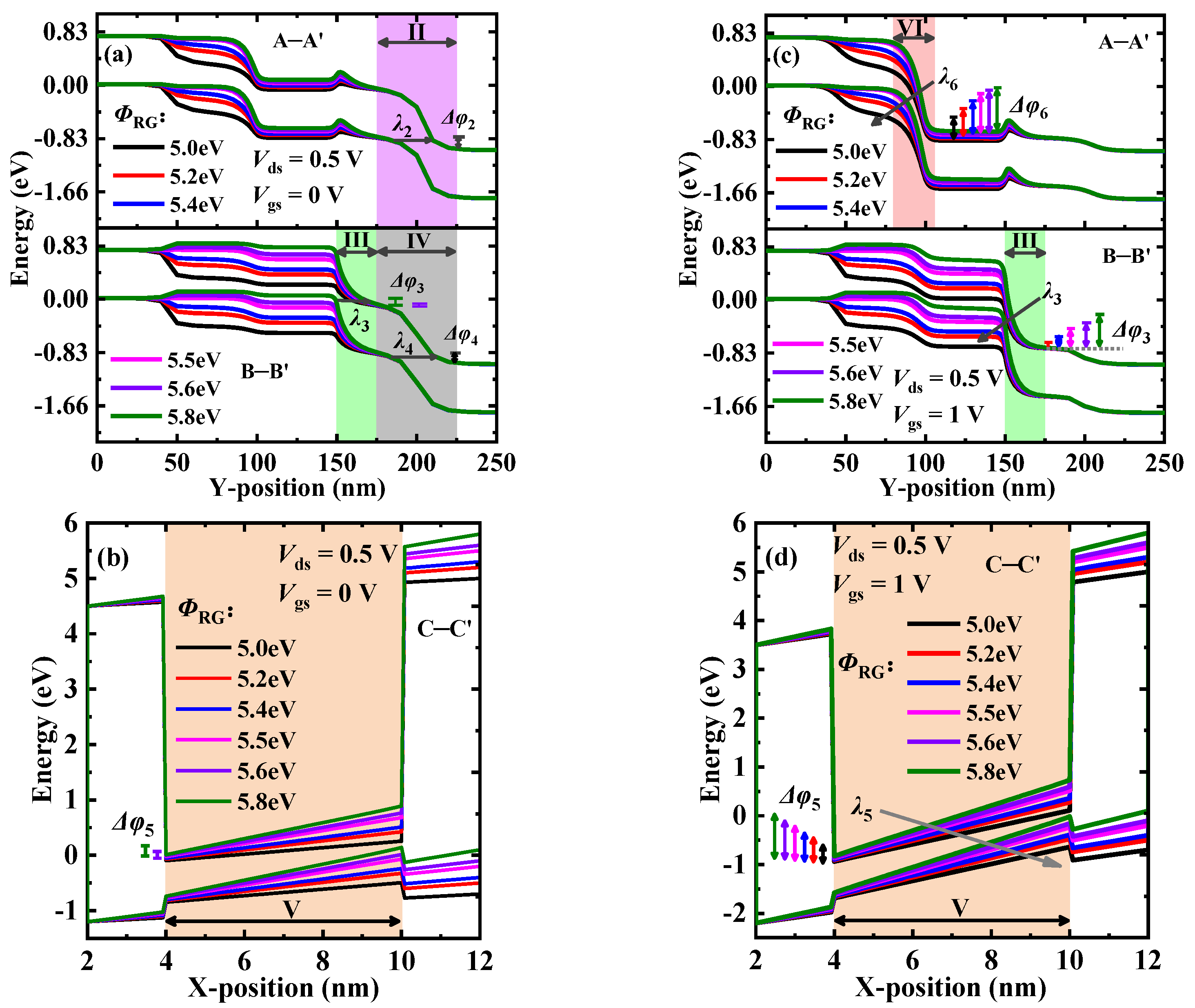
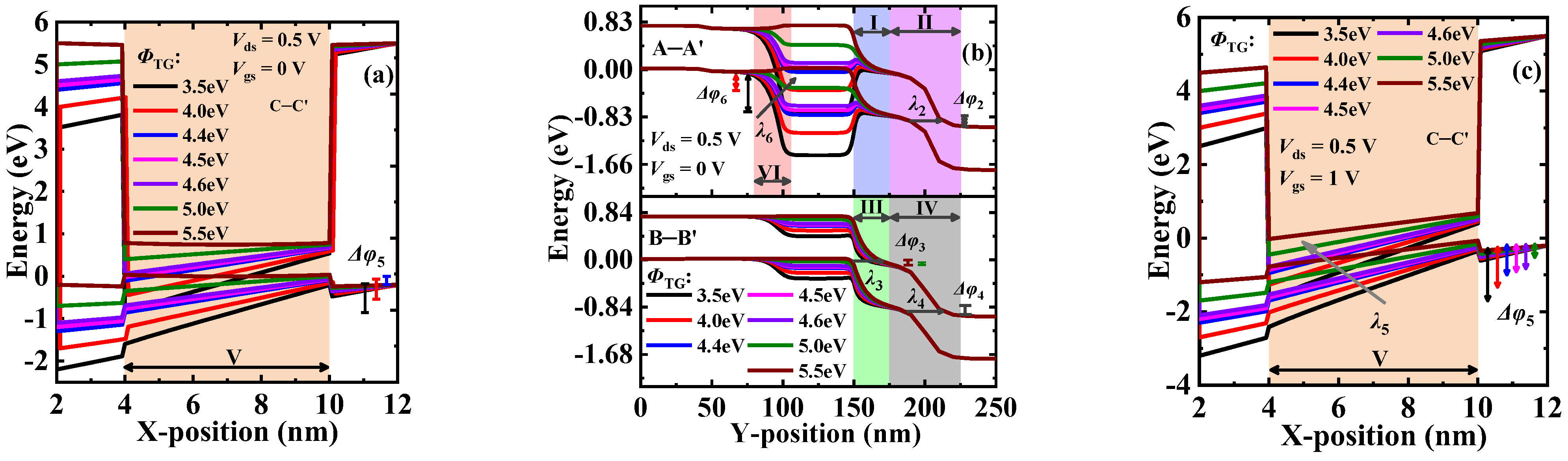
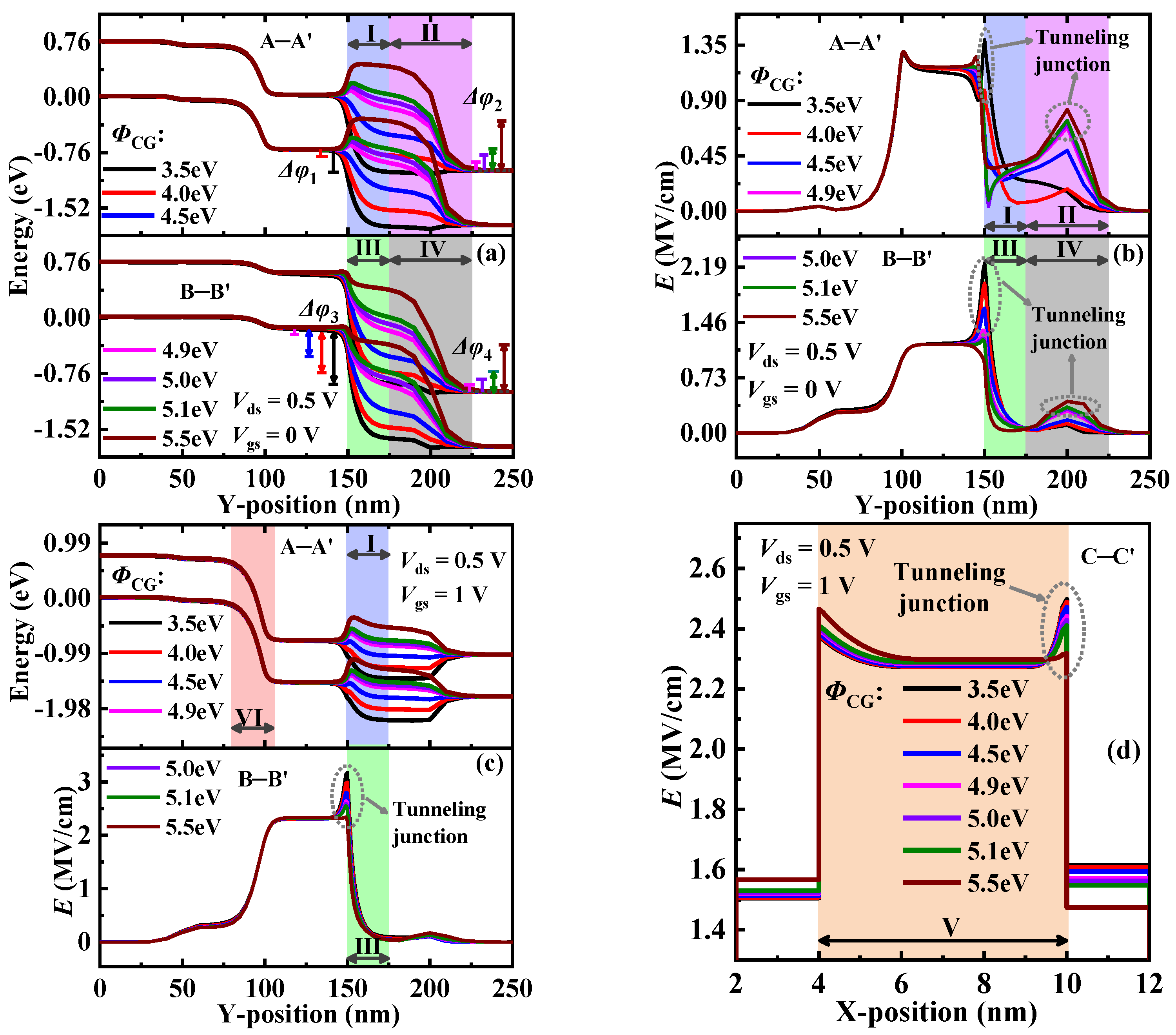
3.4. Effect of Gate Work-Function on DGNP-EHBTFET
4. Conclusions
Author Contributions
Funding
Institutional Review Board Statement
Informed Consent Statement
Data Availability Statement
Conflicts of Interest
References
- Boucart, K.; Ionescu, A.M. Double-gate tunnel fet with high-κ gate dielectric. IEEE Trans. Electron. Devices 2007, 54, 1725–1733. [Google Scholar] [CrossRef]
- Ghosh, B.; Akram, M.W. Junctionless tunnel field effect transistor. IEEE Electron. Device Lett. 2013, 34, 584–586. [Google Scholar] [CrossRef]
- Kumar, M.J.; Janardhanan, S. Doping-less tunnel field effect transistor: Design and investigation. IEEE Trans. Electron. Devices 2013, 60, 3285–3290. [Google Scholar] [CrossRef]
- Kumar, N.; Raman, A. Performance Assessment of the Charge-Plasma-Based Cylindrical GAA Vertical Nanowire TFET with Impact of Interface Trap Charges. IEEE Trans. Electron. Devices 2019, 66, 4453–4460. [Google Scholar] [CrossRef]
- Gupta, A.K.; Raman, A.; Kumar, N. Design and Investigation of a Novel Charge Plasma-Based Core-Shell Ring-TFET: Analog and Linearity Analysis. IEEE Trans. Electron. Devices 2019, 66, 3506–3512. [Google Scholar] [CrossRef]
- Choi, Y.; Hong, Y.; Ko, E.; Shin, C. Optimization of double metal-gate InAs/Si heterojunction nanowire TFET. Semicond. Sci. Technol. 2020, 35, 075024. [Google Scholar] [CrossRef]
- Misra, R.; Singh, K.; Kumar, M.; Rastogi, R.; Kumar, A.; Dubey, S. An Ultra-Low-Power Black Phosphorus (B-Ph)/Si Heterojunction Dopingless-Tunnel FET (HD-TFET) with Enhanced Electrical Characteristics. Superlattices Microstruct. 2021, 149, 106752. [Google Scholar] [CrossRef]
- Tripathy, M.R.; Singh, A.K.; Samad, A.; Chander, S.; Baral, K.; Singh, P.K.; Jit, S. Device and Circuit-Level Assessment of GaSb/Si Heterojunction Vertical Tunnel-FET for Low-Power Applications. IEEE Trans. Electron. Devices 2020, 67, 1285–1292. [Google Scholar] [CrossRef]
- Liu, H.; Yang, L.A.; Jin, Z.; Hao, Y. An In0.53Ga0.47As/In0.52Al0.48As Heterojunction Dopingless Tunnel FET with a Heterogate Dielectric for High Performance. IEEE Trans. Electron. Devices 2019, 66, 3229–3235. [Google Scholar] [CrossRef]
- Pindoo, I.A.; Sinha, S.K.; Chander, S. Improvement of Electrical Characteristics of SiGe Source Based Tunnel FET Device. Silicon 2021, 13, 3209–3215. [Google Scholar] [CrossRef]
- Liu, H.; Yang, L.A.; Chen, Y.; Jin, Z.; Hao, Y. Performance enhancement of the dual-metal gate In0.53Ga0.47As dopingless TFET by using a platinum metal strip insertion. Jpn. J. Appl. Phys. 2019, 58, 104001. [Google Scholar] [CrossRef]
- Gedam, A.; Acharya, B.; Mishra, G.P. Junctionless Silicon Nanotube TFET for Improved DC and Radio Frequency Performance. Silicon 2021, 13, 167–178. [Google Scholar] [CrossRef]
- Raad, B.R.; Tirkey, S.; Sharma, D.; Kondekar, P. A new design approach of dopingless tunnel fet for enhancement of device characteristics. IEEE Trans. Electron. Devices 2017, 64, 1830–1836. [Google Scholar] [CrossRef]
- Liu, H.; Yang, L.A.; Zhang, H.W.; Zhang, B.T.; Zhang, W.T. An In0.53Ga0.47As/In0.52Al0.48As/In0.53Ga0.47As double hetero-junction junctionless TFET. Jpn. J. Appl. Phys. 2021, 60, 074001. [Google Scholar] [CrossRef]
- Xu, H.F.; Han, X.F.; Sun, W. Design and investigation of dopingless double-gate line tunneling transistor: Analog performance, linearity, and harmonic distortion analysis. Chin. Phys. B 2020, 29, 108502. [Google Scholar] [CrossRef]
- Ghosh, P.; Bhowmick, B. Investigation of Electrical Characteristics in a Ferroelectric L-Patterned Gate Dual Tunnel Diode TFET. IEEE Trans. Ultrason. Ferroelectr. Freq. Control 2020, 67, 2440–2444. [Google Scholar] [CrossRef]
- Xie, H.W.; Liu, H.X.; Han, T.; Li, W.; Chen, S.P.; Wang, S.L. TCAD Simulation of a Double L-shaped gate Tunnel Field Effect Transistor with covered source–channel. Micro Nano Lett. 2020, 15, 272–276. [Google Scholar] [CrossRef]
- Ahangari, Z. Performance investigation of steep-slope core–shell nanotube indium nitride electron–hole bilayer tunnel field effect transistor. Appl. Phys. A Mater. Sci. Process. 2019, 125, 405. [Google Scholar] [CrossRef]
- Kim, S.; Choi, W.Y.; Park, B.G. Vertical-Structured Electron-Hole Bilayer Tunnel Field-Effect Transistor for Extremely Low-Power Operation with High Scalability. IEEE Trans. Electron. Devices 2018, 65, 2010–2015. [Google Scholar] [CrossRef]
- Padilla, J.L.; Medina-Bailon, C.; Alper, C.; Gamiz, F.; Ionescu, A.M. Confinement-induced InAs/GaSb heterojunction electron–hole bilayer tunneling field-effect transistor. Appl. Phys. Lett. 2018, 112, 182101. [Google Scholar] [CrossRef]
- Masoudi, A.; Ahangari, Z.; Fathipour, M. Performance optimization of a nanoscale GaSb P-channel electron-hole bilayer tunnel field effect transistor using metal gate workfunction engineering. Mater. Res. Express 2019, 6, 096311. [Google Scholar] [CrossRef]
- Padilla, J.L.; Medina-Bailon, C.; Marquez, C.; Sampedro, C.; Donetti, L.; Gamiz, F.; Ionescu, A.M. Gate Leakage Tunneling Impact on the InAs/GaSb Heterojunction Electron-Hole Bilayer Tunneling Field-Effect Transistor. IEEE Trans. Electron. Devices 2018, 65, 4679–4686. [Google Scholar] [CrossRef]
- Ahangari, Z. Design and performance optimization of thin film tin monoxide (SnO)/silicon electron–hole bilayer tunnel field-effect transistor. J. Comput. Electron. 2020, 19, 1485–1493. [Google Scholar] [CrossRef]
- Shamloo, H.; Goharrizi, A.Y. Performance study of tunneling field effect transistors based on the graphene and phosphorene nanoribbons. Micro Nanostruct. 2022, 169, 207336. [Google Scholar] [CrossRef]
- Jiang, X.; Shi, X.; Zhang, M.; Wang, Y.; Zhang, D.W. A symmetric tunnel field-effect transistor based on mos2/black phosphorus/mos2 nanolayered heterostructures. ACS Appl. Nano Mater. 2019, 2, 5674–5680. [Google Scholar] [CrossRef]
- Jiao, X.; Jia, J.; Shen, L.; Ju, J.; Lee, S. Tunneling field effect transistor integrated with black phosphorus-mos2 junction and ion gel dielectric. Appl. Phys. Lett. 2017, 110, 033103. [Google Scholar]
- Iida, R.; Kim, S.H.; Yokoyama, M.; Taoka, N. Planar-type In0.53Ga0.47As channel band-to-band tunneling metal-oxide-semiconductor field-effect transistors. J. Appl. Phys. 2011, 110, 124505. [Google Scholar] [CrossRef]
- Ahn, D.H.; Yoon, S.H.; Takenaka, M.; Takagi, S. Effects of HfO2/Al2O3 gate stacks on electrical performance of planar InxGa1−xAs tunneling field-effect transistors. Appl. Phys. Express 2017, 10, 084201. [Google Scholar] [CrossRef]
- Seo, J.H.; Yoon, Y.J.; Cho, S.; Kang, I.M.; Lee, J.H. Design optimization and analysis of ingaas/inas/ingaas heterojunction-based electron hole bilayer tunneling fets. J. Nanosci. Nanotechnol. 2019, 19, 6070–6076. [Google Scholar] [CrossRef]
- Alper, C.; Palestri, P.; Padilla, J.L.; Ionescu, A.M. The Electron-Hole Bilayer TFET: Dimensionality Effects and Optimization. IEEE Trans. Electron. Devices 2016, 63, 2603–2609. [Google Scholar] [CrossRef]
- Alper, C.; Palestri, P.; Padilla, J.L.; Ionescu, A.M. Underlap counterdoping as an efficient means to suppress lateral leakage in the electron–hole bilayer tunnel FET. Semicond. Sci. Technol. 2016, 31, 045001. [Google Scholar] [CrossRef]
- Loan, S.A.; Alharbi, A.G.; Rafat, M. Ambipolar leakage suppression in electron–hole bilayer TFET: Investigation and analysis. J. Comput. Electron. 2018, 17, 977–985. [Google Scholar]
- Sahu, C.; Singh, J. Charge-Plasma Based Process Variation Immune Junctionless Transistor. IEEE Electron. Device Lett. 2014, 35, 411–413. [Google Scholar] [CrossRef]
- Hueting, R.J.E.; Rajasekharan, B.; Salm, C.; Schmitz, J. The Charge Plasma P-N Diode. IEEE Electron. Device Lett. 2008, 29, 1367–1369. [Google Scholar] [CrossRef]
- Lide, D.R. CRC Handbook of Chemistry and Physics, 89th ed.; Taylor and Francis: New York, NY, USA, 2008; p. 12. [Google Scholar]
- Kawano, H.; Takahashi, T.; Tagashira, Y.; Mine, H.; Moriyama, M. Work function of refractory metals and its dependence upon working conditions. Surf. Sci. 1999, 146, 105–108. [Google Scholar] [CrossRef]
- Vurgaftman, I.; Meyer, J.R.; Ram-Mohan, L.R. Band parameters for III–V compound semiconductors and their alloys. J. Appl. Phys. 2001, 89, 5815–5875. [Google Scholar] [CrossRef]
- Suzuki, R.; Taoka, N.; Yokoyama, M.; Lee, S.; Kim, S.H.; Hoshii, T.; Yasuda, T.; Jevasuwan, W.; Maeda, T.; Ichikawa, O.; et al. 1-nm-capacitance-equivalent-thickness HfO2/Al2O3/InGaAs metal-oxide-semiconductor structure with low interface trap density and low gate leakage current density. Appl. Phys. Lett. 2012, 100, 132906. [Google Scholar] [CrossRef]
- Zhao, H.; Chen, Y.; Wang, Y.; Zhou, F.; Xue, F.; Lee, J. InGaAs Tunneling Field-Effect-Transistors with Atomic-Layer-Deposited Gate Oxides. IEEE Trans. Electron. Devices 2011, 58, 2990–2995. [Google Scholar] [CrossRef]


| Parameters | Value |
|---|---|
| Bulk material width (W) | 6 nm |
| N+-pocket width (Wp) | 2 nm |
| N+-pocket length (Lp) | 50 nm |
| Drain length (LD) | 50 nm |
| Source length (LS) | 50 nm |
| Tunneling-gate length (LTG) | 50 nm |
| Control-gate length (LCG) | 50 nm |
| Right-gate length (LRG) | 100 nm |
| HfO2 length (LHfO2) | 150 nm |
| SiO2 length (LSiO2) | 100 nm |
| Dielectric width near gate (Wox) | 2 nm |
| Tunneling-gate work-function (ΦTG) | 4.5 eV |
| Control-gate work-function (ΦCG) | 5.0 eV |
| Right-gate work-function (ΦRG) | 5.5 eV |
| ΦRG (eV) | IOFF (A/μm) | ION (A/μm) | ION/IOFF | Vth (V) | SSavg (mV/dec) |
|---|---|---|---|---|---|
| 5.0 | 1.50 × 10⁻¹⁹ | 1.87 × 10⁻⁸ | 1.25 × 10¹¹ | N/A | N/A |
| 5.2 | 1.15 × 10⁻¹⁸ | 1.20 × 10⁻⁶ | 1.04 × 10¹² | 0.52 | 30.7 |
| 5.4 | 2.59 × 10⁻¹⁷ | 5.79 × 10⁻⁶ | 2.24 × 10¹¹ | 0.32 | 33.4 |
| 5.5 | 3.54 × 10⁻¹⁵ | 1.92 × 10⁻⁵ | 5.42 × 10⁹ | 0.17 | 22.8 |
| 5.6 | 2.58 × 10⁻⁹ | 2.87 × 10⁻⁵ | 1.11 × 10⁴ | 0.14 | 88.1 |
| 5.8 | 5.16 × 10⁻⁹ | 4.30 × 10⁻⁵ | 8.33 × 10³ | 0.11 | 85.4 |
| ΦTG (eV) | IOFF (A/μm) | ION (A/μm) | ION/IOFF | Vth (V) | SSavg (mV/dec) |
|---|---|---|---|---|---|
| 3.5 | 1.64 × 10⁻⁷ | 2.19 × 10⁻⁵ | 1.34 × 10² | N/A | N/A |
| 4.0 | 7.87 × 10⁻⁸ | 2.11 × 10⁻⁵ | 2.68 × 10² | 0.02 | 192.3 |
| 4.4 | 7.90 × 10⁻⁹ | 1.99 × 10⁻⁵ | 2.52 × 10³ | 0.12 | 108.9 |
| 4.5 | 3.54 × 10⁻¹⁵ | 1.92 × 10⁻⁵ | 5.42 × 10⁹ | 0.17 | 22.8 |
| 4.6 | 8.51 × 10⁻¹⁵ | 1.81 × 10⁻⁵ | 2.13 × 10⁹ | 0.24 | 33.9 |
| 5.0 | 1.03 × 10⁻¹³ | 9.93 × 10⁻⁶ | 9.64 × 10⁷ | 0.48 | 80.2 |
| 5.5 | 6.86 × 10⁻¹³ | 3.43 × 10⁻⁶ | 5.00 × 10⁶ | 0.51 | 98.8 |
| ΦCG (eV) | IOFF (A/μm) | ION (A/μm) | ION/IOFF | Vth (V) | SSavg (mV/dec) |
|---|---|---|---|---|---|
| 3.5 | 1.47 × 10⁻⁵ | 4.57 × 10⁻⁵ | 3.11 × 100 | N/A | N/A |
| 4.0 | 3.43 × 10⁻⁶ | 3.79 × 10⁻⁵ | 1.10 × 101 | N/A | N/A |
| 4.5 | 9.13 × 10⁻⁸ | 2.90 × 10⁻⁵ | 3.18 × 10² | 0.02 | 506 |
| 4.9 | 4.39 × 10⁻¹² | 2.13 × 10⁻⁵ | 4.85 × 10⁶ | 0.14 | 32.1 |
| 5.0 | 3.54 × 10⁻¹⁵ | 1.92 × 10⁻⁵ | 5.42 × 10⁹ | 0.17 | 22.8 |
| 5.1 | 4.96 × 10⁻¹⁵ | 1.68 × 10⁻⁵ | 3.39 × 10⁹ | 0.23 | 31.5 |
| 5.5 | 7.04 × 10⁻¹⁰ | 6.37 × 10⁻⁶ | 9.05 × 10³ | 0.52 | 105 |
Publisher’s Note: MDPI stays neutral with regard to jurisdictional claims in published maps and institutional affiliations. |
© 2022 by the authors. Licensee MDPI, Basel, Switzerland. This article is an open access article distributed under the terms and conditions of the Creative Commons Attribution (CC BY) license (https://creativecommons.org/licenses/by/4.0/).
Share and Cite
Liu, H.; Zhang, W.; Wang, Z.; Li, Y.; Zhang, H. OFF-State Leakage Suppression in Vertical Electron–Hole Bilayer TFET Using Dual-Metal Left-Gate and N+-Pocket. Materials 2022, 15, 6924. https://doi.org/10.3390/ma15196924
Liu H, Zhang W, Wang Z, Li Y, Zhang H. OFF-State Leakage Suppression in Vertical Electron–Hole Bilayer TFET Using Dual-Metal Left-Gate and N+-Pocket. Materials. 2022; 15(19):6924. https://doi.org/10.3390/ma15196924
Chicago/Turabian StyleLiu, Hu, Wenting Zhang, Zaixing Wang, Yao Li, and Huawei Zhang. 2022. "OFF-State Leakage Suppression in Vertical Electron–Hole Bilayer TFET Using Dual-Metal Left-Gate and N+-Pocket" Materials 15, no. 19: 6924. https://doi.org/10.3390/ma15196924
APA StyleLiu, H., Zhang, W., Wang, Z., Li, Y., & Zhang, H. (2022). OFF-State Leakage Suppression in Vertical Electron–Hole Bilayer TFET Using Dual-Metal Left-Gate and N+-Pocket. Materials, 15(19), 6924. https://doi.org/10.3390/ma15196924