Abstract
2D copper-based semiconductors generally possess low lattice thermal conductivity due to their strong anharmonic scattering and quantum confinement effect, making them promising candidate materials in the field of high-performance thermoelectric devices. In this work, we proposed four 2D copper-based materials, namely CuSbS2, CuSbSe2, CuBiS2, and CuBiSe2. Based on the framework of density functional theory and Boltzmann transport equation, we revealed that the monolayers possess high stability and narrow band gaps of 0.57~1.10 eV. Moreover, the high carrier mobilities (102~103 cm2·V−1·s−1) of these monolayers lead to high conductivities (106~107 Ω−1·m−1) and high-power factors (18.04~47.34 mW/mK2). Besides, as the strong phonon-phonon anharmonic scattering, the monolayers also show ultra-low lattice thermal conductivities of 0.23~3.30 W/mK at 300 K. As results show, all the monolayers for both p-type and n-type simultaneously show high thermoelectric figure of merit (ZT) of about 0.91~1.53 at room temperature.
1. Introduction
Thermoelectric generators can directly convert heat into electrical power, thus attracting wide research interest. Generally, the thermal-electric conversion capacity can be ruled by the dimensionless figure of merit, [1], here S and are the Seebeck coefficient and electrical conductivity, T presents the temperature, and are the electron and lattice thermal conductivity, respectively. Clearly, the ideal thermoelectric material needs to have both high-power factor () and low lattice thermal conductivity. However, this target is not easy to achieve simultaneously as the parameters above are tightly coupled, mutually restricted, and difficult to decouple. They can be regarded as the functions of the vector tensor , energy eigenvalue , and carrier relaxation time [2,3,4]. Besides, the Seebeck coefficient is also closely related to the density of states effective mass () and intrinsic carrier concentration (n), [5]. Additionally, electrical conductivity , and electron thermal conductivity are also restricted by the Wiedemann-Franz-Lorenz’s law, [6], where L is Lorenz number.
In fact, the thermoelectric performance of traditional thermoelectric materials has been effectively improved over the past few decades. Among them, two-dimensional layered (2D) materials, as unique mechanical, electronic, thermal, and optoelectronic properties, as well as quantum confinement effects, make them as promising thermoelectric materials in a variety of applications. For example, quasi-two-dimensional SnSe transistors were revealed to have high Seebeck coefficient, and a field effect mobility of about 250 cm2/Vs at 1.3 K, thus it was found to be a high-quality semiconductor ideal for thermoelectric applications [7]. The 2D Mg3Sb2 monolayer was proved to have a favorable ZT value of 2.5 at 900 K, which is higher than that of its bulk structure. These theoretical results also revealed that nano-engineering can effectively improve the thermoelectric conversion efficiency [8]. Additionally, quasi-two-dimensional GeSbTe compounds were observed by Wei et al. [9]. They found that the monolayer with maximal ZT values of 0.46~0.60 at 750 K, indicating that 2D GeSbTe is a promising mid-temperature thermoelectric material.
Recently, research on the thermoelectric properties of copper-based semiconductors has attracted much attention. For example, Yu et al. [10] proposed a novel phrase 2D σ-Cu2S, which has a low lattice thermal conductivity of 0.10 W/mK, and a high ZT value of 1.33 at 800 K. Cao et al. [11] investigated the electronic structure and thermoelectric performance of β-Cu2Se under strain of −4~4%, they found that its ZT values can reach 1.65~1.71 at 800 K. Other materials, such as Fm-3m Cu2S [12], multi-scale Cu2Se [13], and Cu-Se co-doped Ag2S [14], all exhibited intrinsic low thermal conductivity and high ZT value. In fact, back in 2013 and 2016, Ma and Deng et al. [15,16] investigated the diffusion behavior of Cu in CdTe by density functional theory, they found that Cu s-d orbital coupling only occurred at asymmetric point, but instantly disappeared at symmetric location. These interesting properties make Cu based compound to possess a strong anharmonic scattering, resulting in low intrinsic lattice thermal conductivity. In addition, many semiconductors containing metallic atoms such as Bi have also been reported to possess non-negligible spin-orbit coupling (SOC) effects [17,18], which have the potential to be used in thermoelectric devices. For example, Kim et al. [19] prepared the bulk Bi0.4Sb1.6Te3 alloy via an atomic-layer deposition (ALD) technique, and found that it possesses high ZT values of 1.50 at 329 K. Wu et al. [20] investigated the thermoelectric properties of β-BiAs and β-BiSb monolayers by first-principles calculation and Boltzmann transport theory. They concluded that the monolayers simultaneously exhibit ultra-low lattice thermal conductivities (0.6~0.8 W/mK), and high ZT values (0.78~0.82) at 300 K.
CuMN2 (M = Sb, Bi; N = S, Se) are layered materials with narrow band gaps within ~1.38 eV. [21] Among them, CuSbS2 exhibited the low lattice thermal conductivity of about 1.5~2 W/mK [22]. Additionally, both bulk and monolayer CuSbS2 and CuSbSe2 were revealed to have an excellent thermoelectric power factor at 300 K, reaching about 0.2~1.0 mW/mK2 at constant relaxation time approximation (CRTA) of 11 fs [23]. Therefore, it is of high interest to see whether or not the monolayer CuSbS2, CuSbSe2, CuBiS2, and CuBiSe2, can also deliver good thermoelectric performance. To this end, using first principles calculations, we investigated the electronic structures, mechanical, and transport properties, of these four 2D materials. The calculations revealed that all the monolayers possess narrow band-gaps (0.57~1.10 eV), high power factors (18.04~47.34 mW/mK2), and also low lattice thermal conductivities (0.23~3.30 W/mK). As a result, all the monolayers for both p-type and n-type simultaneously show high ZT values of about 0.91~1.53 at room temperature.
2. Calculation Details
We carried out the calculations in the Vienna Ab initio Simulation Package (VASP) [24], in which the Generalized Gradient Approximation (GGA) [25,26] and Perdew–Burke–Ernzerhof (PBE) functional was adopted to exchange-correlation approximation. To shorten the computation time, we used the HipHive [27] code to extract the second and third order force-constants (IFCs). Besides, we used the Phonopy [28] code to calculate the Grüneisen parameters and phonon dispersion, and employed the Phono3py [29] to evaluate the phonon scattering rate and lattice thermal conductivity. We also used the Wannier90 [30] code to solve Boltzmann transport equation, and then characterized the thermoelectric properties as a function of the chemical potential.
The transport properties, such as electrical conductivity, electron thermal conductivity and ZT value, are directly related to carrier relaxation time, therefore, we used the deformation potential theory (DPT) to calculate carrier mobility, and further corrected it by the acoustic phonon-limited method (APM), which is more suitable for anisotropic materials. See Supplementary Materials for more calculation details.
3. Results and Discussion
3.1. Crystal Structures
The crystal structures of CuMN2 (M = Sb, Bi; N = S, Se) for bulk and single-layer are shown in Figure 1. As can be seen, the bulk CuMN2 are layered structures, similar to graphite and MoS2. Therefore, we first investigated the cleavage energy of their single-layers, and its calculation method was based on the latest Rigorous Method proposed by Jung et al. [31]. , where and are energies of single-layer and bulk unit-cell, and are the in-plane area and the number of the slab in a bulk-unit. The calculation results are listed in Table S1. The corresponding cleavage energies are within 0.68~0.93 J/m2, which are higher than those of graphene (0.33 J/m2), black phosphorus (BP) (0.36 J/m2), and MoS2 (0.27 J/m2) [32], but still lower than those of single-layer Ca2N (1.09 J/m2) [33], GeP3 (1.14 J/m2), and InP3 (1.32 J/m2) [34]. All of these results indicate the feasibility of obtaining single-layer CuMN2 by mechanical exfoliation in experiments. The lattice constants and thicknesses of the monolayers after structural relaxation are listed in Table 1. Owing to each atomic radius satisfies: S (1.03 Å) < Se (1.16 Å) < Cu (1.28 Å) < Sb (1.61 Å) < Bi (1.82 Å), both the lattice constants (a/b) and thickness (h) follow the order of CuSbS2 < CuBiS2 < CuSbSe2 < CuBiSe2.
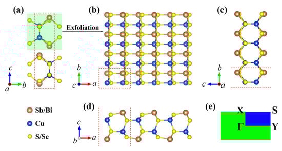
Figure 1.
The structures of: (a) bulk; (b) top view; (c,d) side view; and (e) K-point path of 2D CuMN2 (M = Sb, Bi; N = S, Se).

Table 1.
The structural parameters, buckling height h, cleavage energies Ef, and band gaps Eg of 2D CuMN2 (M = Sb, Bi; N = S, Se).
3.2. Elastic Properties and Stability
In general, for a new 2D material, we can identify its mechanical stability by its elastic constants . As listed in Table 2, all the monolayers satisfy the Born-Huang criterion, and [35], indicating that they all possess high mechanical stability. Additionally, since the structures of the monolayers are anisotropic, . We further calculated the Young’s moduli and Poisson’s ratio of these materials [36], as shown in Figure 2. Here is the angle with respect to a-axis. As can be seen, their Young’s moduli are relatively close, showing the maximum values of 58.20~66.52 N/m in the direction of 0° (180°) and the minimum values of 28.34~33.04 N/m in the direction of 90° (270°), which are obviously lower than those of graphene (350 ± 3.15 N/m) [37], h-BN ((270 N/m), [38] and MoS2 (200 N/m) [39]. Such low Young’s moduli are expected to exhibit low lattice thermal conductivity [40]. On the contrary, the Poisson’s ratio minimizes in both 0° and 90° directions, and maximizes at 40° (140°) with values of 0.14~0.34, respectively. Fantastically, monolayer CuSbS2 and CuBiS2 are rare auxetic materials with negative Poisson’s ratio (NPR) of −0.02 and −0.04 at 0° (180°). Such interesting NPR phenomenon is also observed in PN (−0.08) [41], and tetra-silicene (−0.06) [42], which have been revealed to hold high potential in medicine, defense, and the escalation of tensions [43].
Table 2.
The Elastic constants , the maximums for Young’s modulus Y and Poisson’s ratio υ, and Debye temperature of 2D CuMN2 (M = Sb, Bi; N = S, Se).
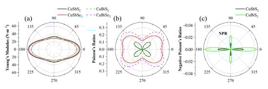
Figure 2.
(a) The Young’s moduli: (b) Poisson’s ratio; and (c) NPR of 2D CuMN2 (M = Sb, Bi; N = S, Se).
We also investigated the bonding strength of materials by calculating their electron localization function (ELF) and Bader charge analysis (see Figure S1 and Table S2 for more details). Clearly, the adjacent atoms exhibit a predominant ionic bond characteristic. However, the net charge transfer is relatively few, mostly within ~1.0 e, indicating that they have relatively weak bond strength and thus exhibit low Young’s moduli. Besides, we analyzed the thermal stabilities of these four materials at different temperatures by using ab initio molecular dynamics (AIMD) simulations [44]. We revealed that they can remain high stability at 500 K, as their crystal structure does not bond breaking or undergo remodeling, as showed in Figure S2 in Supplementary Materials.
3.3. Electronic Structures
To accurately characterize the electronic structures of the monolayers, we first analyze the effect of spin-orbit coupling (SOC) on their electronic band structures. As shown in Figure S3, SOC has a non-ignorable impact on band structure, especially for CuBiS2 and CuBiSe2, so SOC was all considered in following calculations. As shown in Figure 3, all the monolayers are narrow band-gap semiconductors with band gaps of 0.57~1.10 eV, which are slightly smaller than or comparable to their bulk structures [21,23,45,46]. Since the valence band maximum (VBM) and conduction band minimum (CBM) are both located at Γ point, both CuSbS2, CuSbSe2, and CuBiS2 belong to direct bandgap semiconductors. However, for CuBiSe2, its VBM is transferred to between Y and Γ, so it is an indirect bandgap semiconductor. Moreover, as show in Figure S4, the VBMs are mainly composed of S-3p/Se-4p and Cu-3d electrons, while CBMs are mainly composed of Sb-5p/Bi-6p and S-3p/Se-4p electrons. In addition, the total density of states for both VBMs and CBMs showed relatively steep distribution, indicating that the monolayers have high density of states effective mass, and thus to possess both high p-type and n-type Seebeck coefficients, as shown in Figure 4.
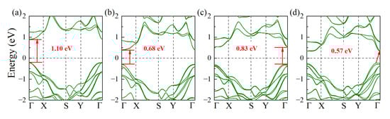
Figure 3.
Band structures of monolayer: (a) CuSbS2; (b) CuSbSe2; (c) CuBiS2; and (d) CuBiSe2 at HSE 06 + SOC functional.
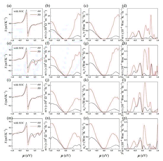
Figure 4.
Electron transport properties of 2D CuMN2 (M = Sb, Bi; N = S, Se): (a,e,i,m) Seebeck coefficients; (b,f,j,n) electrical conductivities; (c,g,k,o) electron thermal conductivities; and (d,h,l,p) power factors along a—(black line) and b—directions (red line) with PBE + SOC functional.
Next, we explored the carrier mobility of electrons and holes along the a- and b-axis of the monolayers (see Figures S5 and S6, and Table S3 for more details). For monolayer CuSbS2, CuSbSe2, and CuBiS2, their effective masses (me) of electrons are higher than those of holes (mh) along a-axis, corresponding to their flatter band near CBMs than VBMs along the Γ–X direction. However, the opposite is true for CuBiSe2, the me (0.93 m0) is indeed lower than mh (2.83 m0), which can be interpreted as the steeper dispersion curve corresponding to its VBM between Γ and X. Besides, for all monolayers, their elastic modulus (C2D) along the a-axis is larger than that along b-axis, which is consistent with their elastic constants. Further, the deformation potential constant (El) fluctuates widely from 0.75 eV to 4.48 eV, and the lower El occur simultaneously for the hole along the a-axis. As a result, the hole mobilities in the a-axis are higher than those in other cases, and the highest is even up to 4562.47 cm2·V−1·s−1 for CuSbS2. Since DPT method tends to overestimate the mobility of semiconductor, especially when the El is relatively small [35], we adopted the APT method to correct the results, as listed in Table 3. Clearly, after corrected by APT, the carrier mobility increases when the El is relatively large, and decreases otherwise. As can be seen, the mobilities of both electrons (μe) and holes (μh) are basically in the range of 102~103 cm2·V−1·s−1, in which CuSbS2 and CuSbSe2 exhibit the highest μh and μe of 1661.49 and 937.12 cm2·V−1·s−1, which are far higher than that of MoS2 (μh ~200 cm2·V−1·s−1) [47], but lower than those of silicene (μe ~105 cm2·V−1·s−1) [48], and phosphorene (μh ~104 cm2·V−1·s−1) [49].
Table 3.
The carrier effective mass (m*/m0), deformation potential constant (El/eV), plane stiffness (C2D/N·m−1), hole (μh/cm2·V−1·s−1) and electron mobility (μe/cm2·V−1·s−1), and relaxation time (τ/fs) of the monolayers under PBE + SOC functional at 300 K.
3.4. Electrical Transport Properties
Furthermore, we explored the electron transport properties of the monolayers by solving Boltzmann transport equation, as show in Figure 4 (see Figure S7 for more details about maximally localized Wannier functions (MLWFs)). Obviously, the maximums of Seebeck coefficient (S) satisfy CuSbS2 > CuBiS2 > CuSbSe2 > CuBiSe2, which consist with their band-gaps ordering, as small gap implies high carrier concentration. Coincidentally, the p-type Seebeck coefficients are higher than those of n-type in a-axis, but opposite in the b-axis, which may be caused by the anisotropy of the density of states effective mass. Besides, constrained by the Wiedemann-Franz-Lorenz’s law [3], the electronic thermal conductivity and electrical conductivity have similar curves. In general, electron transport properties are directly related to the carrier relaxation time (). Therefore, we further calculated it by using the formula [50], here , , and e are carrier effective mass, mobility, and electron charge, as listed in Table 3. After taking the relaxation time, the monolayers exhibit high electrical conductivity of up to 106~107 Ω−1·m−1, also high PF of 18.04~47.34 mW·K−2·m−1 at 300 K (see Table 4), which are higher than or comparable to those of their bulk structures (0.8~1.0 mW/mK2) [23], Pd2Se3 (1.21~1.61 mW·K−2·m−1) [6], PdSe2 (5~25 mW·K−2·m−1) [51], and Tl2O (10~33 mW·K−2·m−1) [52].
Table 4.
The maximums of Seebeck coefficient S (mV·K), electron thermal conductivity (W·m−1·K−1), electrical conductivity σ (×106 Ω−1·m−1), lattice thermal conductivity (W·m−1·K−1), PF (mW·K−2·m−1) and ZT values in the chemical potential of −1 eV~1 eV at 300 K.
3.5. Phonon Transport Properties
The phonon dispersions are shown in Figure 5, where the red, green, blue, and pink curves denote the out-of-plane acoustic (ZA), longitudinal acoustic (LA), transverse acoustic (TA), and optical phonons, respectively. As can be seen, these phonon dispersions have no virtual frequencies, indicating that these four monolayers have high kinetic stability. As the Sb(Bi) atoms are heavier than the others, they show lower phonon frequencies, while the lighter S(Se) atoms possess higher frequencies. Meanwhile, there is some coupling between in-plane (XY) and out-of-plane phonons (ZZ) for all atoms, which can be attributed to the fact that each atom is dispersed in multiple layers (see Figure 1), which breaks the plane symmetry of their structure and allows more phonons to participate in scattering [53]. Additionally, the lowest optical mode boundary frequencies at Γ point of the monolayers are within 0.42~0.89 THz, which are close to those of SnSe (~0.99 THz) [54], KAgS (~1.20 THz) [50], and PbSe (~0.63 THz) [55], indicating that their optical modes softening is relatively severe, as in these materials with intrinsic low thermal conductivity. Further, the low-frequency optical modes at Γ points are caused by the antiparallel motions of the outer Sb/Bi and S/Se atoms, which can effectively increase the phonon dissipation and further reduce the phonon lifetime [55]. Comparatively, for monolayer CuSbSe2 and CuBiSe2, their phonon frequencies are relatively lower, and more coupling occurs in the low frequency range, resulting in their scattering free path is shorter, and thus have lower phonon lifetimes.
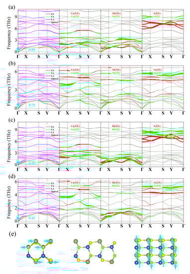
Figure 5.
The orbital-resolved phonon dispersion of: (a) CuSbS2; (b) CuSbSe2; (c) CuBiS2; (d) CuBiSe2; where the XY and ZZ denote the in-plane and out-of-plane phonons; and (e) the schematic diagram of low frequency optical phonon at Γ point for monolayer CuSbS2, where the arrows represent the direction of the vibration.
The lattice thermal conductivity, , can be expressed as the volumetric specific heat , group velocity , and phonon lifetime , respectively. The group velocity , can also be calculated by the first derivative of frequency with respect to the wave vector q [38]. As seen in Figure 6a–d, the LA modes for all the monolayers exhibit maximum group velocities of 2.06~3.59 km/s, smaller than those of Arsenene and Antimonene (~4.5 km/s) [56], BP (~8.6 km/s) [57], and MoS2 (~6.5 km/s) [58]. Although the optical modes also exhibit large group velocities in high frequency region, their phonon lifetime is very small, almost zero, as shown in Figure 6e–h, so the of these monolayers are mainly contributed by acoustic modes. In addition, for monolayer CuSbSe2 and CuBiSe2, their phonon lifetimes are significantly shorter than those of the others, which is mainly due to their strong coupling at low frequency phonons, as analyzed above.
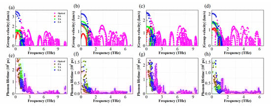
Figure 6.
Group velocities (a–d) and phonon lifetimes (e–h) of 2D CuMN2 (M = Sb, Bi; N = S, Se), here the red, blue, green, and pink dot correspond to ZA, LA, TA, and Optical phonons, respectively.
Generally, we can use the Grüneisen parameters γ to describe the anharmonic interactions of a material, which is effective mean to analyze the physical nature of lattice thermal conductivity. It can be obtained from the relationship of phonon frequency and volume as [59]. For a large indicates the strong phonon-phonon anharmonic scattering, resulting in a low intrinsic . As shown in Figure 7, all the monolayers exhibited the high in the low frequency range, which are similar to that of KAgX (X = S, Se) [50]. Obviously, CuSbSe2 and CuBiSe2 exhibited larger values than those of CuSbS2 and CuBiS2, and thus have inherently stronger anharmonic interactions, as well as lower . Moreover, the negative γ indicate that these materials may have negative thermal expansion (NTE) properties [4].
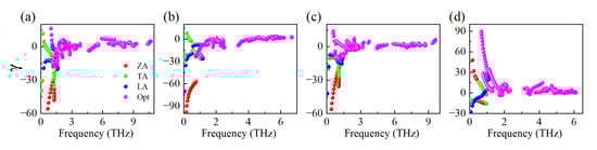
Figure 7.
The Grüneisen parameters γ for monolayer: (a) CuSbS2; (b) CuSbSe2; (c) CuBiS2; and (d) CuBiSe2.
Although the volumetric specific heat is also directly related to the , the difference is very small, especially as the temperature increases, as seen in Figure 8a. As a result, all the materials exhibit low within ~3.30 W·m−1·K−1, with CuSbSe2 and CuBiSe2 having lower values due to stronger phonon anharmonic interactions and low phonon lifetimes. Additionally, we can notice that the is higher in a-axis, which can be attributed to the stronger bonding, as well as higher Young’s moduli in this direction, and thus better heat transport. As shown in Figure 8b and Table 4, the monolayers show the low lattice thermal conductivities of 0.23~3.30 W·m−1·K−1 at 300 K, which are comparable to or lower than those of bilayer SnSe (0.9 W·m−1·K−1) [60], Tl2O (0.9~1.2 W·m−1·K−1) [52], Tetradymites (1.2~2.1 W·m−1·K−1) [61], and Antimonene (5 W·m−1·K−1) [56].
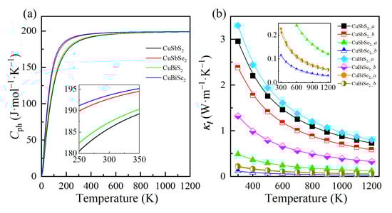
Figure 8.
(a) The volumetric specific heat, and (b) lattice thermal conductivity of 2D CuMN2 (M = Sb, Bi; N = S, Se).
3.6. Thermoelectric Figure of Merit
Finally, we fitted the thermoelectric figure of merit (ZT) of these four monolayers at 300 K, as shown in Figure 9 (see Figures S8 and S9 for more details about the thermoelectric properties at without SOC functional). Obviously, the monolayers exhibit higher p-type ZT values in a-axis, while higher n-type ZT in b-axis, which is consistent with the results of higher hole mobility in the a-axis, while higher electron mobility in b-axis. As listed in Table 4, the monolayers simultaneously exhibit high ZT values for p-type of 0.91~1.17, and n-type of 0.74~1.53 at 300 K, which are higher than or comparable to those of many 2D thermoelectric materials, such as Pd2Se3 (0.9) [6], Tellurene (0.6) [62], InSe (0.5) [63], and SnSe (0.5) [64].
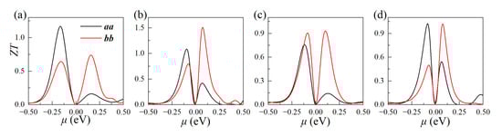
Figure 9.
ZT values of the monolayer: (a) CuSbS2; (b) CuSbSe2; (c) CuBiS2; and (d) CuBiSe2 at 300 K.
4. Conclusions
In this work, we investigated the stability, mechanical, electrical, and phonon transport properties of 2D CuMN2 (M = Sb, Bi; N = S, Se). We found that monolayers possess the acceptable cleavage energies of 0.68~0.93 J/m2, and narrow band-gaps of 0.57~1.10 eV, respectively. Based on the acoustic phonon-limited method, we revealed that the electron and hole mobility are basically in the range of 102~103 cm2·V−1·s−1. Besides, they also have high electrical conductivity of 106~107 Ω−1·m−1, high PF of 18.04~47.34 mW·K−2·m−1 at 300 K. Furthermore, due to the stronger phonon anharmonic interactions and low phonon lifetimes, their lattice thermal conductivities are as low as 0.23~3.30 Wm−1 K−1. As a result, all the monolayers simultaneously exhibit high ZT values for p-type of 0.91~1.17, and n-type of 0.74~1.53 at 300 K, indicating that they have potential applications in nano-electronic and thermoelectric devices.
Supplementary Materials
The following supporting information can be downloaded at: https://www.mdpi.com/article/10.3390/ma15196700/s1, Table S1: The cleavage energies, Figure S1: the Electron Localization Functions, Figure S2: the ab initio molecules dynamics simulation, Table S2: Bader charge analysis results, Figure S3: the band structures at PBE functional without and with SOC functional, Figure S4: the partial density of states, Figure S5, Table S3, Figure S6: the details on carrier mobility calculations, Figure S7: the MLWFs calculated by Wannnier90 code, Figures S8 and S9: the thermoelectric properties of monolayer CuMN2 (M = Sb, Bi; N = S, Se) without SOC functional.
Author Contributions
W.F. and Y.C.: conceptualization, formal analysis, validation, visualization, writing—review and editing. K.K.: formal analysis, validation, visualization, data curation, methodology. M.L.: supervision, funding acquisition, software, project administration, writing—review and editing. All authors have read and agreed to the published version of the manuscript.
Funding
We gratefully acknowledge the financial support from the National Key R&D Program of China (Grant No. 2019YFB1503500), the National Natural Science Foundation of China (Grant Nos. 61874040, 11774082 and 11975093), the Natural Science Foundation of Hubei Province (Grant Nos. 2019CFA006 and 2021EHB005), and the Program for Science and Technology Innovation Team in Colleges of Hubei Province (Grant No. T201901).
Institutional Review Board Statement
Not applicable.
Informed Consent Statement
Not applicable.
Data Availability Statement
The data presented in this study are available on request from the corresponding authors. The data are not publicly available due to ongoing research in the project.
Conflicts of Interest
The authors declare no conflict of interest.
References
- Wang, S.F.; Zhang, Z.G.; Wang, B.T.; Zhang, J.R.; Wang, F.W. Intrinsic Ultralow Lattice Thermal Conductivity in the Full-Heusler Compound Ba2AgSb. Phys. Rev. Appl. 2022, 17, 034023. [Google Scholar] [CrossRef]
- Gao, Z.; Liu, G.; Ren, J. High Thermoelectric Performance in Two-Dimensional Tellurium: An Ab Initio Study. ACS Appl. Mater. Interfaces 2018, 10, 40702–40709. [Google Scholar] [CrossRef] [PubMed]
- Fang, W.; Wei, H.; Xiao, X.; Chen, Y.; Kuang, K.; Li, M.; He, Y. XTlO (X = K, Rb, Cs): Novel 2D semiconductors with high electron mobilities, ultra-low lattice thermal conductivities and high thermoelectric figures of merit at room temperature. Appl. Surf. Sci. 2022, 599, 153924. [Google Scholar] [CrossRef]
- Fang, W.; Wei, H.; Xiao, X.; Chen, Y.; Li, M.; He, Y. Monolayer SnX (X = O, S, Se): Two-Dimensional Materials with Low Lattice Thermal Conductivities and High Thermoelectric Figures of Merit. ACS Appl. Energy Mater. 2022, 5, 7802–7812. [Google Scholar] [CrossRef]
- Wu, Y.; Xu, K.; Ma, C.; Chen, Y.; Lu, Z.; Zhang, H.; Fang, Z.; Zhang, R. Ultrahigh carrier mobilities and high thermoelectric performance at room temperature optimized by strain-engineering to two-dimensional aw-antimonene. Nano Energy 2019, 63, 103870. [Google Scholar] [CrossRef]
- Naghavi, S.S.; He, J.; Xia, Y.; Wolverton, C. Pd2Se3 Monolayer: A Promising Two-Dimensional Thermoelectric Material with Ultralow Lattice Thermal Conductivity and High Power Factor. Chem. Mater. 2018, 30, 5639–5647. [Google Scholar] [CrossRef]
- Tayari, V.; Senkovskiy, B.V.; Rybkovskiy, D.; Ehlen, N.; Fedorov, A.; Chen, C.Y.; Avila, J.; Asensio, M.; Perucchi, A.; di Pietro, P.; et al. Quasi-two-dimensional thermoelectricity in SnSe. Phys. Rev. B 2018, 97, 136. [Google Scholar] [CrossRef]
- Huang, S.; Wang, Z.; Xiong, R.; Yu, H.; Shi, J. Significant enhancement in thermoelectric performance of Mg3Sb2 from bulk to two-dimensional mono layer. Nano Energy 2019, 62, 212–219. [Google Scholar] [CrossRef]
- Wei, T.-R.; Hu, P.; Chen, H.; Zhao, K.; Qiu, P.; Shi, X.; Chen, L. Quasi-two-dimensional GeSbTe compounds as promising thermoelectric materials with anisotropic transport properties. Appl. Phys. Lett. 2019, 114, 053903. [Google Scholar] [CrossRef]
- Yu, J.; Li, T.; Nie, G.; Zhang, B.P.; Sun, Q. Ultralow lattice thermal conductivity induced high thermoelectric performance in the delta-Cu2S monolayer. Nanoscale 2019, 11, 10306–10313. [Google Scholar] [CrossRef]
- Cao, W.; Wang, Z.; Miao, L.; Shi, J.; Xiong, R. Thermoelectric Properties of Strained beta-Cu2Se. ACS Appl. Mater. Interfaces 2021, 13, 34367–34373. [Google Scholar] [CrossRef] [PubMed]
- Yao, Y.; Zhang, B.P.; Pei, J.; Liu, Y.C.; Li, J.F. Thermoelectric performance enhancement of Cu2S by Se doping leading to a simultaneous power factor increase and thermal conductivity reduction. J. Mater. Chem. C 2017, 5, 7845–7852. [Google Scholar] [CrossRef]
- Bo, L.; Li, F.J.; Hou, Y.B.; Zuo, M.; Zhao, D.G. Enhanced Thermoelectric Performance of Cu2Se via Nanostructure and Compositional Gradient. Nanomaterials 2022, 12, 640. [Google Scholar] [CrossRef] [PubMed]
- Li, L.W.; Peng, C.X.; Chen, J.; Ma, Z.; Chen, Y.Q.; Li, S.Y.; Wang, J.L.; Wang, C. Study the effect of alloying on the phase transition behavior and thermoelectric properties of Ag2S. J. Alloys Compd. 2021, 886, 161241. [Google Scholar] [CrossRef]
- Ma, J.; Wei, S.H. Origin of Novel Diffusions of Cu and Ag in Semiconductors: The Case of CdTe. Phys. Rev. Lett. 2013, 110, 235901. [Google Scholar] [CrossRef]
- Deng, H.X.; Luo, J.W.; Li, S.S.; Wei, S.H. Origin of the Distinct Diffusion Behaviors of Cu and Ag in Covalent and Ionic Semiconductors. Phys. Rev. Lett. 2016, 117, 165901. [Google Scholar] [CrossRef]
- Freitas, R.R.Q.; Mota, F.D.; Rivelino, R.; de Castilho, C.M.C.; Kakanakova-Georgieva, A.; Gueorguiev, G.K. Spin-orbit-induced gap modification in buckled honeycomb XBi and XBi3 (X = B, Al, Ga, and In) sheets. J. Phys. Condens. Mater 2015, 27, 485306. [Google Scholar] [CrossRef]
- dos Santos, R.B.; Rivelino, R.; Mota, F.D.; Kakanakova-Georgieva, A.; Gueorguiev, G.K. Feasibility of novel (H3C)(n)X(SiH3)(3-n) compounds (X = B, Al, Ga, In): Structure, stability, reactivity, and Raman characterization from ab initio calculations. Dalton Trans. 2015, 44, 3356–3366. [Google Scholar] [CrossRef]
- Kim, K.C.; Lim, S.S.; Lee, S.H.; Hong, J.; Cho, D.Y.; Mohamed, A.Y.; Koo, C.M.; Baek, S.H.; Kim, J.S.; Kim, S.K. Precision Interface Engineering of an Atomic Layer in Bulk Bi2Te3 Alloys for High Thermoelectric Performance. ACS Nano 2019, 13, 7146–7154. [Google Scholar] [CrossRef]
- Wu, C.Y.; Sun, L.; Han, J.C.; Gong, H.R. Band structure, phonon spectrum, and thermoelectric properties of beta-BiAs and beta-BiSb monolayers. J. Mater. Chem. C 2020, 8, 581–590. [Google Scholar] [CrossRef]
- Gassoumi, A.; Alfaify, S.; Ben Nasr, T.; Bouarissa, N. The investigation of crystal structure, elastic and optoelectronic properties of CuSbS2 and CuBiS2 compounds for photovoltaic applications. J. Alloys Compd. 2017, 725, 181–189. [Google Scholar] [CrossRef]
- Parker, D.; Singh, D.J. Transport properties of hole-doped CuBiS2. Phys. Rev. B 2011, 83, 233206. [Google Scholar] [CrossRef]
- Alsaleh, N.M.; Singh, N.; Schwingenschlögl, U. Role of interlayer coupling for the power factor of CuSbS2 and CuSbSe2. Phys. Rev. B 2016, 94, 125440. [Google Scholar] [CrossRef]
- Hafner, J. Ab-initio simulations of materials using VASP: Density-functional theory and beyond. J. Comput. Chem. 2008, 29, 2044–2078. [Google Scholar] [CrossRef]
- Blochl, P.E. Projector augmented-wave method. Phys. Rev. B 1994, 50, 17953–17979. [Google Scholar] [CrossRef]
- Zhang, T.; Li, M.K.; Chen, J.; Wang, Y.; Miao, L.S.; Lu, Y.M.; He, Y.B. Multi-component ZnO alloys: Bandgap engineering, hetero-structures, and optoelectronic devices. Mater. Sci. Eng. R 2022, 147, 100661. [Google Scholar] [CrossRef]
- Eriksson, F.; Fransson, E.; Erhart, P. The Hiphive Package for the Extraction of High-Order Force Constants by Machine Learning. Adv. Theory Simul. 2019, 2, 1800184. [Google Scholar] [CrossRef]
- Togo, A.; Tanaka, I. First principles phonon calculations in materials science. Scripta Mater. 2015, 108, 1–5. [Google Scholar] [CrossRef]
- Togo, A.; Chaput, L.; Tanaka, I. Distributions of phonon lifetimes in Brillouin zones. Phys. Rev. B 2015, 91, 094306. [Google Scholar] [CrossRef]
- Pizzi, G.; Vitale, V.; Arita, R.; Blugel, S.; Freimuth, F.; Geranton, G.; Gibertini, M.; Gresch, D.; Johnson, C.; Koretsune, T.; et al. Wannier90 as a community code: New features and applications. J. Phys. Condens. Matter 2020, 32, 165902. [Google Scholar] [CrossRef]
- Jung, J.H.; Park, C.H.; Ihm, J. A Rigorous Method of Calculating Exfoliation Energies from First Principles. Nano Lett. 2018, 18, 2759–2765. [Google Scholar] [CrossRef] [PubMed]
- Song, Y.Q.; Yuan, J.H.; Li, L.H.; Xu, M.; Wang, J.F.; Xue, K.H.; Miao, X.S. KTlO: A metal shrouded 2D semiconductor with high carrier mobility and tunable magnetism. Nanoscale 2019, 11, 1131–1139. [Google Scholar] [CrossRef] [PubMed]
- Zhao, S.; Li, Z.; Yang, J. Obtaining two-dimensional electron gas in free space without resorting to electron doping: An electride based design. J. Am. Chem. Soc. 2014, 136, 13313–13318. [Google Scholar] [CrossRef] [PubMed]
- Zhang, P.; Yuan, J.-H.; Fang, W.-Y.; Li, G.; Wang, J. Two-dimensional V-shaped PdI2: Auxetic semiconductor with ultralow lattice thermal conductivity and ultrafast alkali ion mobility. Appl. Surf. Sci. 2022, 601, 154176. [Google Scholar] [CrossRef]
- Fang, W.Y.; Li, P.A.; Yuan, J.H.; Xue, K.H.; Wang, J.F. Nb2SiTe4 and Nb2GeTe4: Unexplored 2D Ternary Layered Tellurides with High Stability, Narrow Band Gap and High Electron Mobility. J. Electron. Mater. 2020, 49, 959–968. [Google Scholar] [CrossRef]
- Xiong, W.Q.; Huang, K.X.; Yuan, S.J. The mechanical, electronic and optical properties of two-dimensional transition metal chalcogenides MX2 and M2X3 (M = Ni, Pd; X = S, Se, Te) with hexagonal and orthorhombic structures. J. Mater. Chem. C 2019, 7, 13518–13525. [Google Scholar] [CrossRef]
- Lajevardipour, A.; Neek-Amal, M.; Peeters, F.M. Thermomechanical properties of graphene: Valence force field model approach. J. Phys. Condens. Matter 2012, 24, 175303. [Google Scholar] [CrossRef]
- Fang, W.Y.; Xiao, X.L.; Wei, H.R.; Chen, Y.; Li, M.K.; He, Y.B. The elastic, electron, phonon, and vibrational properties of monolayer XO2 (X = Cr, Mo, W) from first principles calculations. Mater. Today Commun. 2022, 30, 103183. [Google Scholar] [CrossRef]
- Fang, W.Y.; Yue, C.; Pan, Y.; Wei, H.R.; Xiao, X.L.; Li, M.K.; Rajeev, A.; He, Y.B. Elastic constants, electronic structures and thermal conductivity of monolayer XO2 (X = Ni, Pd, Pt). Acta Phys. Sin. 2021, 70, 246301. [Google Scholar] [CrossRef]
- Xie, Q.Y.; Liu, P.F.; Ma, J.J.; Kuang, F.G.; Zhang, K.W.; Wang, B.T. Monolayer SnI2: An Excellent p-Type Thermoelectric Material with Ultralow Lattice Thermal Conductivity. Materials 2022, 15, 3147. [Google Scholar] [CrossRef]
- Xiao, W.Z.; Xiao, G.; Rong, Q.Y.; Wang, L.L. Theoretical discovery of novel two-dimensional V-A-N binary compounds with auxiticity. Phys. Chem. Chem. Phys. 2018, 20, 22027–22037. [Google Scholar] [CrossRef] [PubMed]
- Qiao, M.; Wang, Y.; Li, Y.F.; Chen, Z.F. Tetra-silicene: A Semiconducting Allotrope of Silicene with Negative Poisson’s Ratios. J. Phys. Chem. C 2017, 121, 9627–9633. [Google Scholar] [CrossRef]
- Peng, R.; Ma, Y.; He, Z.; Huang, B.; Kou, L.; Dai, Y. Single-Layer Ag2S: A Two-Dimensional Bidirectional Auxetic Semiconductor. Nano Lett. 2019, 19, 1227–1233. [Google Scholar] [CrossRef]
- Yuan, J.H.; Yu, N.N.; Xue, K.H.; Miao, X.S. Stability, electronic and thermodynamic properties of aluminene from first-principles calculations. Appl. Surf. Sci. 2017, 409, 85–90. [Google Scholar] [CrossRef]
- Wada, T.; Maeda, T. Optical properties and electronic structures of CuSbS2, CuSbSe2, and CuSb(S1−xSex)2 solid solution. Phys. Status Solidi C 2017, 14, 1600196. [Google Scholar] [CrossRef]
- Prudhvi Raju, N.; Thangavel, R. Theoretical investigation of spin–orbit coupling on structural, electronic and optical properties for CuAB2 (A = Sb, Bi; B = S, Se) compounds using Tran–Blaha-modified Becke–Johnson method: A first-principles approach. J. Alloys Compd. 2020, 830, 154621. [Google Scholar] [CrossRef]
- Zeng, L.; Xin, Z.; Chen, S.W.; Du, G.; Kang, J.F.; Liu, X.Y. Phonon-Limited Electron Mobility in Single-Layer MoS2. Chin. Phys. Lett. 2014, 31, 027301. [Google Scholar] [CrossRef]
- Shao, Z.G.; Ye, X.S.; Yang, L.; Wang, C.L. First-principles calculation of intrinsic carrier mobility of silicene. J. Appl. Phys. 2013, 114, 093712. [Google Scholar] [CrossRef]
- Pu, C.Y.; Yu, J.H.; Yu, R.M.; Tang, X.; Zhou, D.W. Hydrogenated PtP2 monolayer: Theoretical predictions on the structure and charge carrier mobility. J. Mater. Chem. C 2019, 7, 12231–12239. [Google Scholar] [CrossRef]
- Zhu, X.L.; Yang, H.Y.; Zhou, W.X.; Wang, B.T.; Xu, N.; Xie, G.F. KAgX (X = S, Se): High-Performance Layered Thermoelectric Materials for Medium-Temperature Applications. ACS Appl. Mater. Interfaces 2020, 12, 36102–36109. [Google Scholar] [CrossRef]
- Qin, D.; Yan, P.; Ding, G.; Ge, X.; Song, H.; Gao, G. Monolayer PdSe2: A promising two-dimensional thermoelectric material. Sci. Rep. 2018, 8, 2764. [Google Scholar] [CrossRef] [PubMed]
- Huang, H.H.; Xing, G.; Fan, X.; Singh, D.J.; Zheng, W.T. Layered Tl2O: A model thermoelectric material. J. Mater. Chem. C 2019, 7, 5094–5103. [Google Scholar] [CrossRef]
- Huang, L.F.; Gong, P.L.; Zeng, Z. Correlation between structure, phonon spectra, thermal expansion, and thermomechanics of single-layer MoS2. Phys. Rev. B 2014, 90, 045409. [Google Scholar] [CrossRef]
- Li, C.W.; Hong, J.; May, A.F.; Bansal, D.; Chi, S.; Hong, T.; Ehlers, G.; Delaire, O. Orbitally driven giant phonon anharmonicity in SnSe. Nat. Phys. 2015, 11, 1063. [Google Scholar] [CrossRef]
- Liu, P.F.; Bo, T.; Xu, J.P.; Yin, W.; Zhang, J.R.; Wang, F.W.; Eriksson, O.; Wang, B.T. First-principles calculations of the ultralow thermal conductivity in two-dimensional group-IV selenides. Phys. Rev. B 2018, 98, 235426. [Google Scholar] [CrossRef]
- Sharma, S.; Kumar, S.; Schwingenschlögl, U. Arsenene and Antimonene: Two-Dimensional Materials with High Thermoelectric Figures of Merit. Phys. Rev. Appl. 2017, 8, 044013. [Google Scholar] [CrossRef]
- Zhu, L.Y.; Zhang, G.; Li, B.W. Coexistence of size-dependent and size-independent thermal conductivities in phosphorene. Phys. Rev. B 2014, 90, 214302. [Google Scholar] [CrossRef]
- Hong, Y.; Zhang, J.C.; Zeng, X.C. Thermal Conductivity of Monolayer MoSe2 and MoS2. J. Phys. Chem. C 2016, 120, 26067–26075. [Google Scholar] [CrossRef]
- Xie, Q.Y.; Ma, J.J.; Liu, Q.Y.; Liu, P.F.; Zhang, P.; Zhang, K.W.; Wang, B.T. Low thermal conductivity and high performance anisotropic thermoelectric properties of XSe (X = Cu, Ag, Au) monolayers. Phys. Chem. Chem. Phys. 2022, 24, 7303–7310. [Google Scholar] [CrossRef]
- Hung, N.T.; Nugraha, A.R.T.; Saito, R. Designing high-performance thermoelectrics in two-dimensional tetradymites. Nano Energy 2019, 58, 743–749. [Google Scholar] [CrossRef]
- Nag, S.; Saini, A.; Singh, R.; Kumar, R. Ultralow lattice thermal conductivity and anisotropic thermoelectric performance of AA stacked SnSe bilayer. Appl. Surf. Sci. 2020, 512, 145640. [Google Scholar] [CrossRef]
- Sharma, S.; Singh, N.; Schwingenschlögl, U. Two-Dimensional Tellurene as Excellent Thermoelectric Material. ACS Appl. Energy Mater. 2018, 1, 1950–1954. [Google Scholar] [CrossRef]
- Hung, N.T.; Nugraha, A.R.T.; Saito, R. Two-dimensional InSe as a potential thermoelectric material. Appl. Phys. Lett. 2017, 111, 092107. [Google Scholar] [CrossRef]
- Wang, F.Q.; Zhang, S.H.; Yu, J.B.; Wang, Q. Thermoelectric properties of single-layered SnSe sheet. Nanoscale 2015, 7, 15962–15970. [Google Scholar] [CrossRef] [PubMed]
Publisher’s Note: MDPI stays neutral with regard to jurisdictional claims in published maps and institutional affiliations. |
© 2022 by the authors. Licensee MDPI, Basel, Switzerland. This article is an open access article distributed under the terms and conditions of the Creative Commons Attribution (CC BY) license (https://creativecommons.org/licenses/by/4.0/).