Article

Temperature-Dependent Absorption of Ternary HfS2−xSex 2D Layered Semiconductors

1
Department of Electronic Engineering, National Changhua University of Education, Changhua City 50074, Taiwan
2
Department of Electronic Engineering, Ming Chi University of Technology, New Taipei City 243, Taiwan
3
Department of Physics, National Changhua University of Education, Changhua City 500207, Taiwan
4
Department of Electronic Engineering, Chienkuo Technology University, Changhua City 500020, Taiwan
5
Department of Experimental Physics, Faculty of Fundamental Problems of Technology, Wrocław University of Science and Technology, 50370 Wrocław, Poland
*
Author to whom correspondence should be addressed.
Materials 2022, 15(18), 6304; https://doi.org/10.3390/ma15186304
Submission received: 5 August 2022 / Revised: 27 August 2022 / Accepted: 7 September 2022 / Published: 11 September 2022

Abstract

:
In this study, we present the investigation of optical properties on a series of HfS2−xSex crystals with different Se compositions x changing from 0 to 2. We used the chemical-vapor transport method to grow these layered ternary compound semiconductors in bulk form. Their lattice constants and crystal properties were characterized by X-ray diffraction, high-resolution transmission electron microscopy, and Raman spectroscopy. We have performed absorption spectroscopies to determine their optical band-gap energies, which started from 2.012 eV with x = 0, and gradually shifts to 1.219 eV for x = 2. Furthermore, we measured the absorption spectroscopies at different temperatures in the range of 20–300 K to identify the temperature dependence of band-gap energies. The band-gap energies of HfS2−xSex were determined from the linear extrapolation method. We have noticed that the band-gap energy may be continuously tuned to the required energy by manipulating the ratio of S and Se. The parameters that describe the temperature influence on the band-gap energy are evaluated and discussed.

1. Introduction

There is a great need for high-speed electronics with low power consummation beyond the silicon-based devices. New flexible materials for electronics and optoelectronics applications with an atomic scale thickness have resulted in much exploration [1,2,3]. Novel two dimensional (2D) materials have attracted significant interest because of their unique fundamental properties [4,5]. Layered 2D transition metal dichalcogenides (TMDs) materials with the chemical formula MX2 (here M represents the transition metal and X represents a chalcogen) are considered to be candidates for next-generation electronic circuit applications. 2D TMD is stacked layer by layer in the form of X-M-X, consisting of two hexagonal planes of chalcogen elements [6]. The chalcogen layer-by-layer structure by van der Waals (vdW) interacts to form the bulk material, which allows for atomic control of its ultrathin thickness [7,8]. Unlike graphene without a band gap, the 2D TMDs with semiconductor behaviors can be adopted to the integration of electronic devices [9]. Up to now, 2D MX2 (M = Mo or W and X = S or Se) of single- or multi-layered TMDs with ultrathin thickness have been research topics of the fields of material science and nanotechnology [10]. Due to their specific optical and physical properties, the investigations of various device structures have included the heterostructure p-n junction diode [11], field effect transistor [12,13], fin-shaped field effect transistor [14,15], phototransistor [16], energy storage and conversion [17,18], sensors [19,20], biomedicine [21,22,23], and water remediation [24,25].
Among these TMDs materials, only a few studies on HfX2 (X = S or Se) compounds have been achieved [26]. The HfX2-based TMDs have high work function [27] and high mobility [28], allowing for their potential applications in nanoelectronic and optoelectronic devices [29,30,31,32]. The thermoelectric performance of HfS2 is also investigated [33]. The heterostructure of graphene/HfS2 as an electrode material for alkali-ion batteries is also performed [34]. However, the band gap of HfS2 and HfSe2 is fixed with no flexibility, which limits its ability in applications in devices. The bad gap of mixed ternary alloys can be tuned by adjusting the composition ratio, which allows for a wider detecting range in optoelectronic device applications. Due to the wide range of possible applications, the detailed temperature dependence of band-gap transitions is still unclear. Hence, more studies on the HfS2−xSex alloys concentrated on the temperature dependence of band-gap transitions are essential to pave the way for next-generation device applications.
In this study, the investigation of the structural properties of HfS2−xSex alloys measured by X-ray diffraction (XRD), high-resolution transmission electron microscopy (HRTEM), and Raman spectroscopy has been presented. We also characterized their compositions by electron probe X-ray micro-analyzer (EPMA). The band-gap energy determination of HfS2−xSex mixed crystals was carried out by the absorption spectroscopy. The parameters corresponding to the temperature dependence of the band-gap energies were also evaluated and discussed.

2. Experimental

Layered HfS2−xSex single crystals in bulk form were grown using the chemical-vapor transport method. I2 (~3.63 mg/cm3) was used as a transport agent for chemical transportation. A quartz ampoule with the size of 30 mm OD × 25 mm ID × 28 cm was used to contain the high-purity (Hf: 99.99%, S: 99.99%, and Se: 99.99%) constituent elements, which were weighted to fit the atomic ratio HfS2−xSex (0 ≤ x ≤ 2). A high-vacuum diffusion pump was used to maintained the quartz ampoule pressure at approximately 2 × 10⁻⁵ torr during the sealing process. Then, it was put into a two-zone furnace and two automatic temperature controllers were used to control the heater to hold the high temperature zone at 800 °C, and the low temperature zone at 650 °C in a duration of 14 days. The crystals thus grown have a surface area up to 10~20 mm2 and are 20–100 µm thick. In this work, the nominal composition x of six HfS2−xSex crystals varied as 0, 0.4, 0.8, 1.2, 1.6, and 2. The lattice structure and alloy compositions for all the HfS2−xSex crystals were checked by XRD and EPMA, respectively. The measured composition of the HfS2−xSex alloys by EPMA is listed in Table 1. The Raman spectroscopy has been performed on 3D Nanometer Scale Raman spectrometer (Tokyo Instruments, Nanofinder 30) with 488 nm laser. The laser power was set at about 1 mW to avoid the heating damages. The HRTEM images and selected area electron diffraction (SAED) patterns were taken by PHILIPS CM-200 TWIN FE-TEM to characterize the lattice structure of HfS2−xSex crystals.
The optical properties of the HfS2−xSex layered single crystals were studied by absorption measurements in the temperature range of 20–300 K. The light source with a 150 W quartz-halogen lamp was adopted to a PTI 0.25 m grating monochromator, focused on the sample with near-normal light incidence and collected by a silicon photodetector. The temperature-dependent measurements were carried out by a closed-cycle cryogenic refrigerator equipped with a digital thermometer controller with temperature stability in 0.5 K.

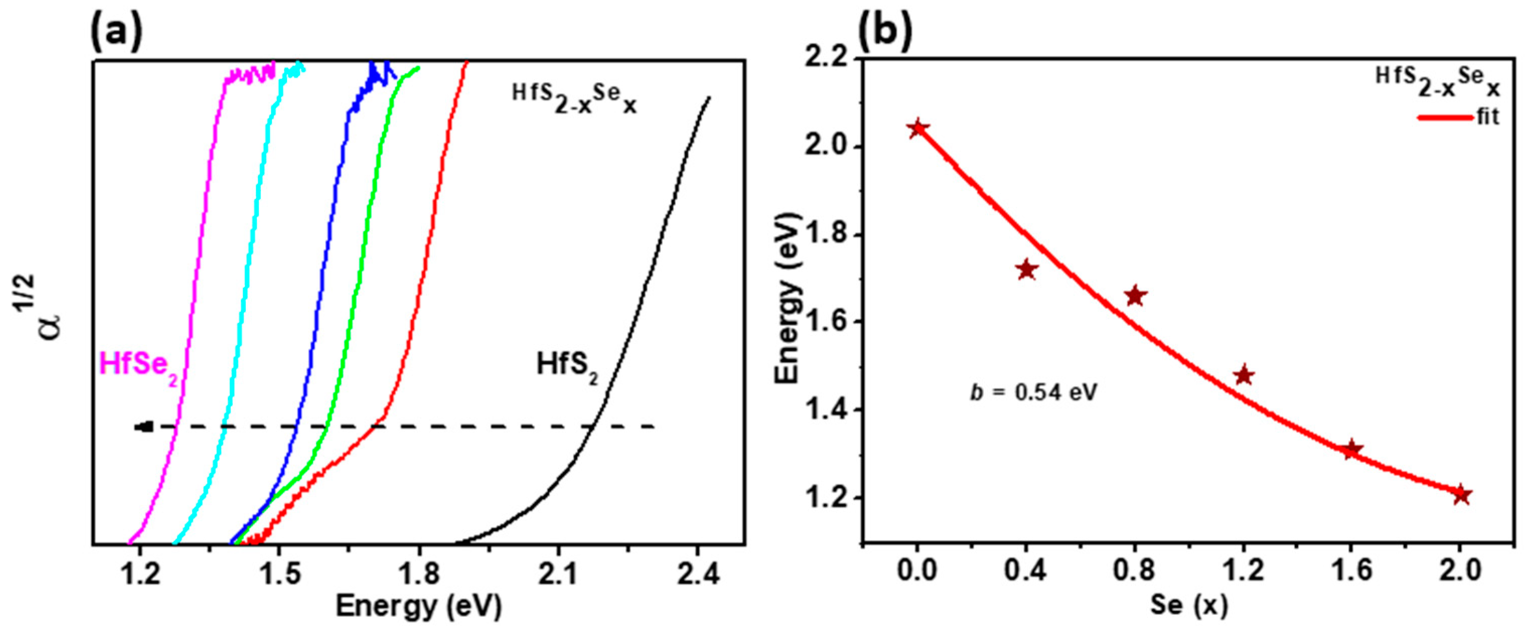
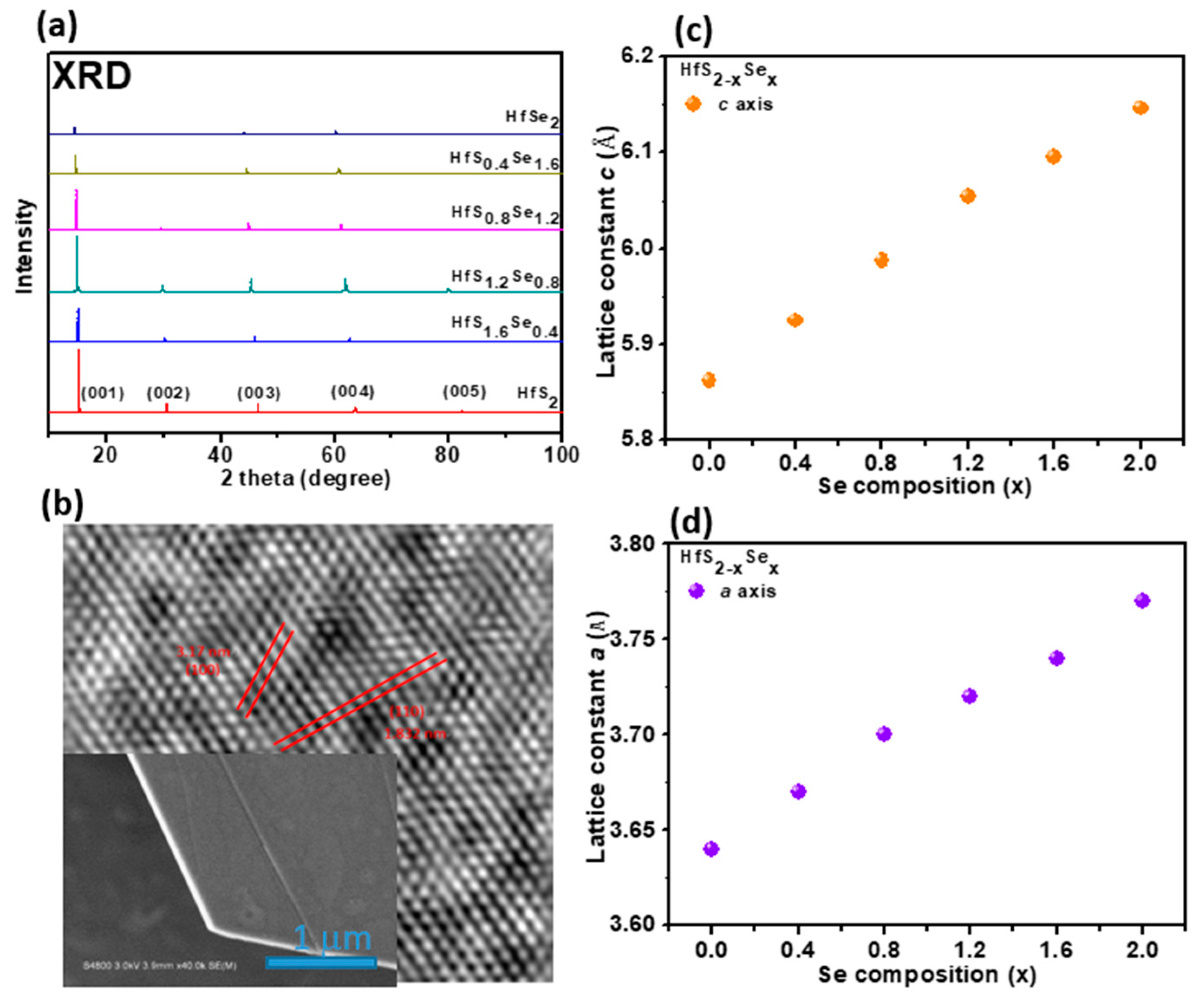
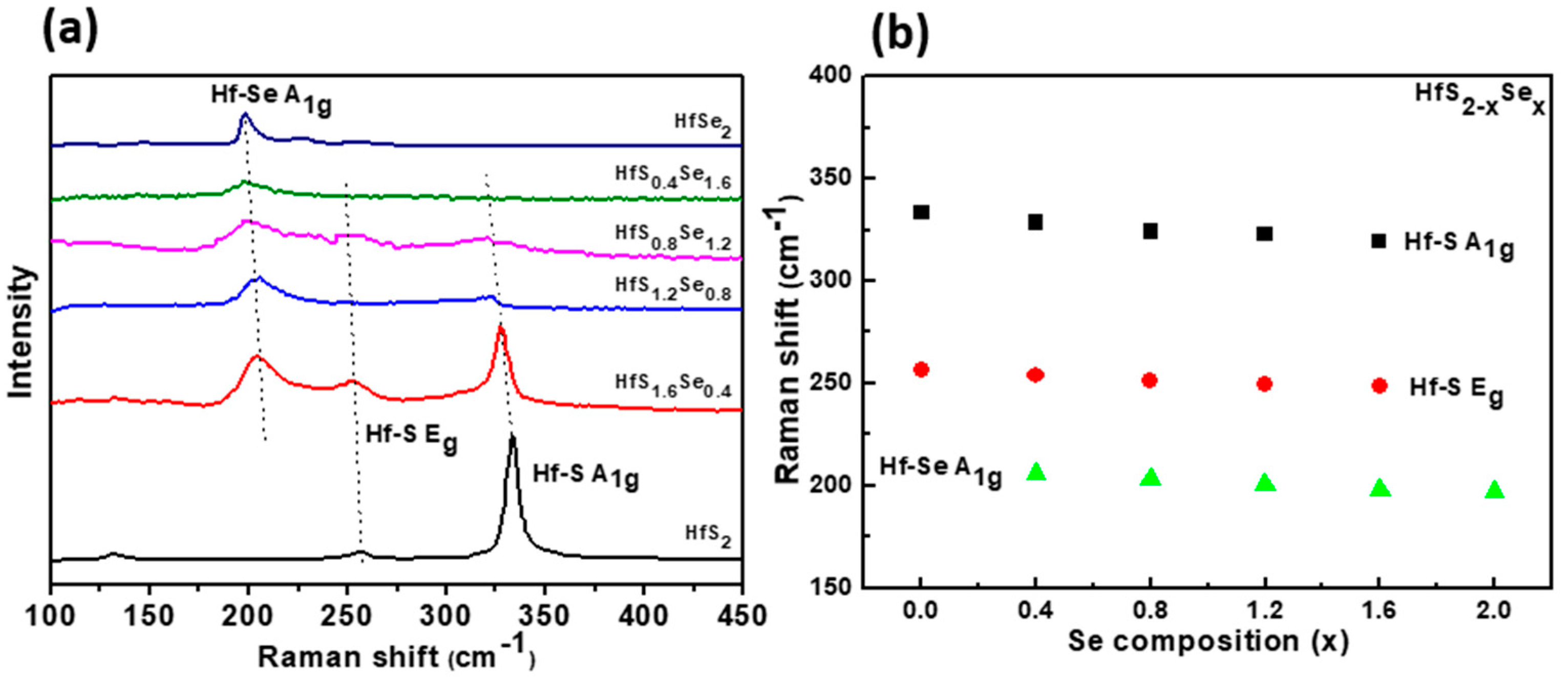
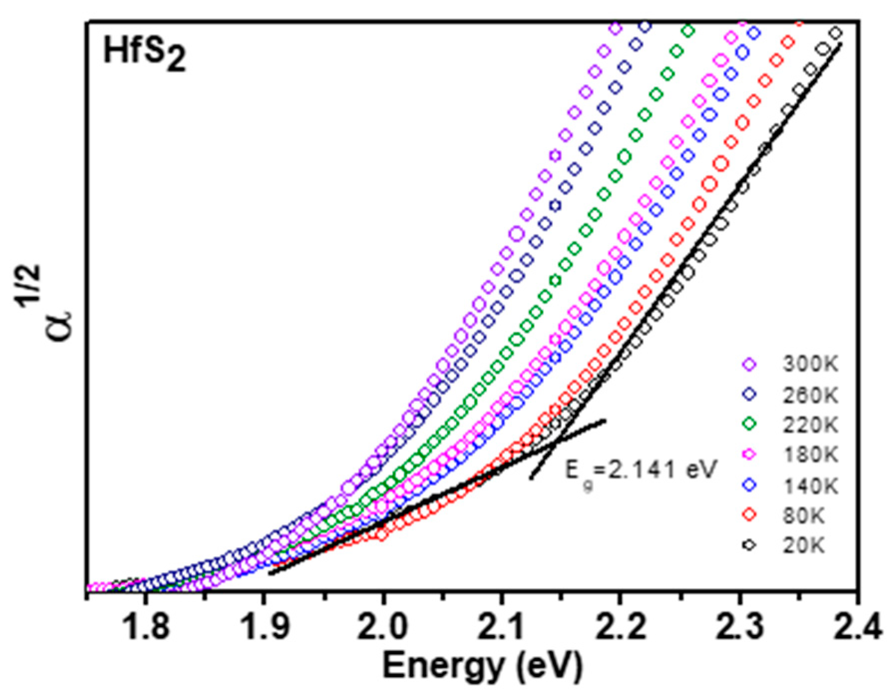
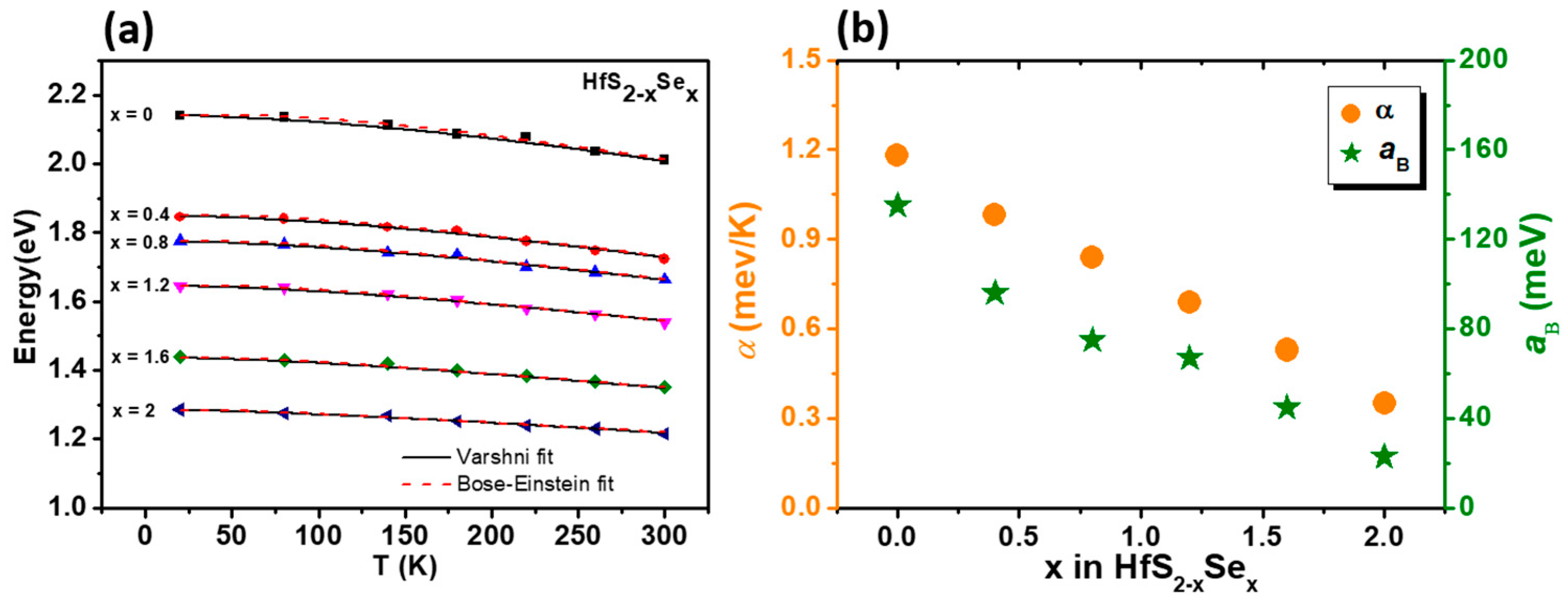
3. Results and Discussion

The XRD patterns of HfS2−xSex layered single crystals with various Se content are depicted in Figure 1a. The major diffraction peaks of HfS2−xSex crystals fit in the figure of the CdI2 type hexagonal unit cell with the Pbnm space group. The strongest diffraction peak is assigned to the (001) plane; other diffraction peaks are assigned to the (002), (003), (004), and (005) planes [35]. The main peak position of the HfS2−xSex layered single crystals shifts to a lower angle gradually with increasing Se. The lattice constant c of HfS2−xSex crystals can be deduced according to Bragg’s law [36]. All of the XRD peaks, which are indicated as (001) to (005) from left to right, are derived from different planes stacking perpendicularly to the c-axis. Because all the XRD peaks indicate the same orientation, this result confirms the single crystalline nature of our HfS2−xSex crystal. In Equation (1) with the first-order approximation n = 1, and for the (001) orientation XRD peak located at 2θ ≈ 15° for the HfS2, we can find that d001 = 0.5862 nm. The lattice constant c can be deduced by substituting (hlk) = (001) into the Equation (2); we can see that the c value is equal to the value of d001, which is 0.5862 nm for HfS2 and gradually increases to 0.6146 nm for HfSe2.
2dsinθ = n λ
1 d 2 h k l = 4 3 ( h 2 + h k + k 2 a 2 ) + l 2 c 2
Figure 1b indicates the lattice constant c values deduced from XRD diffraction. The c value is 0.5862 nm for HfS2 and gradually increases to 0.6146 nm for HfSe2. The HfS2−xSex crystal structure was also characterized by HRTEM. Figure 1c shows the HRTEM image of HfS1.6Se0.4 crystal. The deduced lattice constants a of HfS2−xSex crystals from HRTEM are plotted in Figure 1d. The above results indicate that the crystal stoichiometry is in agreement with the nominal value.
Figure 2a shows the characterization results of HfS2−xSex layered single crystals probed by Raman spectroscopy. The composition-dependent vibration modes of HfS2−xSex layered single crystals were assigned as A1g (Hf-Se), Eg (Hf-S), and A1g (Hf-S). The intensity of Hf-S related Raman modes decreases with increasing Se composition, and the vibration modes of Hf-Se are enhanced gradually. In Figure 2b, the Raman vibration modes of the HfS2−xSex layered single crystals are statistically depicted. The Raman frequencies of the A1g and Eg vibration modes with increasing Se composition show a red-shift behavior. The Raman frequency shifts and intensity evolution with the S/Se atomic ratio are consistent with the reported literature [37] (HfS2−xSex alloys). The XRD measurements and Raman spectroscopy provide characterizations for the identification of the crystal structure and material phases of the HfS2−xSex layered single crystals.
The room temperature absorption spectra of HfS2−xSex layered single crystals with various Se contents of x = 0, 0.4, 0.8, 1.2, 1.6, and 2, respectively, are shown in Figure 3a. We can observe that the absorption edge gradually shifts to a lower energy side with increasing Se content. The atomic number of Se is larger than S, which causes the band gap decrease with increasing Se content in HfS2−xSex layered single crystals. The band-gap energies (Eg) for HfS2−xSex layered single crystals with different Se content were determined from the extrapolation of the absorption coefficient to the base line. The obtained band-gap energy values of HfS2−xSex layered single crystals at 300 K are 2.012, 1.729, 1.664, 1.543, 1.349, and 1.219 eV for Se content of x = 0, 0.4, 0.8, 1.2, 1.6, and 2, respectively. Compared to the band gap determined by the theoretical study of the HfS2−xSex monolayer, the results in study are in reasonable agreement with the reported theoretical results [38]. The discrepancy might be due to the material thickness effects and the difference between the experimental and the theoretical model. The composition dependence of the band-gap energy describes the degree of nonlinearity that can be fitted by the expression Eg(x) = (x/2)Eg(HfSe2) + (1 − (x/2))Eg(HfS2) − bx/2(1 − (x/2)) [36], where Eg is the band-gap energy and b is the bowing parameter. In Figure 3b, the solid line represents the fit of experimental data with above equation. In this work, b is determined to be 0.54 eV, which is comparable with previous results of 0.68 eV for SnSSe [39] and 0.456 eV for ZnSSe [40] alloys. The deduced bowing parameters in this work are smaller than that the values 0.74–1.84 eV for the III-nitrides semiconductors. This might be due to the fact that the bowing parameter is dominated by various physical effects, structural and chemical disorder, atomic mismatch, strain, and carrier concentration [41].
Displayed by dotted curves in Figure 4 are the experimental absorption spectra of the HfS2 layered single crystals at several temperatures between 20 and 300 K. There are a number of methods for bandgap calculation using absorption data, such as Tauc’s method, by taking α1/2 (indirect bandgap) or α2 (direct bandgap) methods. The relation derived by Tauc et al. [42] was intended for use with amorphous materials. They assume that the amorphous materials contain a localization of energy states; thus, absorption transitions do not need to conserve momentum. For single crystals with indirect energy gaps, the electron transition from the valence band to the conduction band, which is also understood as absorption transition, can be described by Fermi’s golden rule. The density states on both the valence and conduction bands will be included with phonon interactions to follow the rule of momentum conservation. The square root of the absorption coefficient plot could be available to extract the indirect band-gap energy [43]. As a general characteristic of most semiconductors, when the measurement temperature gradually rises, the band-gap energy exhibits a red-shift. The temperature variation of the band-gap energies obtained from the absorption measurements for the HfS2−xSex ternary-layered single crystals are plotted in Figure 5. The temperature-dependent evolution of the band-gap energy of the HfS2−xSex ternary-layered single crystals can be described by the Varshni semi-empirical model [44]:
Eg(T) = Eg(0) − αT2/(β + T)
where Eg(0) is the band-gap energies at 0 K. The constant α is related to the electron (exciton)–average phonon interaction strength, and β is closely related to the Debye temperature. The solid curves are least-squares fits to the Varshni semi-empirical model. Obtained from the fitting procedure, the Varshni parameters for the investigated crystals and, for comparison, other layered crystals such as MoSSe, WSSe 2D-layered semiconductors [45], III–V group semiconductors such as GaAs [46] and InP [47], II–VI group semiconductors such as ZnSe [48], and IV group semiconductors such as Si [46] are listed in Table 2.
The temperature dependence of band-gap energies can also be described by an expression containing the Bose–Einstein occupation factor for phonons [49,50]:
Eg (T) = Eg (0) − 2aB/[exp(ΘB /T) − 1]
where Eg(0) is the band-gap energy at 0 K, aB represents the strength of the electron (exciton)–average phonon interaction, and ΘB corresponds to the average phonon temperature. In solid crystals, phonons play an important role in many physical properties. The variation of band-gap energy with temperature is majorly affected by lattice dilation and the electron–phonon interaction, which can be correlated with the phonon interaction [51,52].
The results obtained from fitting the parameter values according to the Bose–Einstein expression are listed in Table 2 as well.
The electron–phonon interaction strength parameter α from Varshni model can be easily related to electron–phonon interaction constant aB and average phonon temperature ΘB from Bose–Einstein expression by taking the high-temperature limit of both expressions. This yields α = 2aBB. Obtained from the fitting procedure to the experimental data with both expressions, the parameters presented in Table 2 show that this relation is matched. From Equation (4), it is straightforward to show that the high temperature limit of the slope of E(T) vs. the T curve approaches a value of −2aBB. The calculated value of −2aBB for band-gap transition energies equals 0.78, −0.66, −0.58, −0.53, −0.42, and −0.28 meV/K for Se contents (x) = 0, 0.4, 0.8, 1.2, 1.6, and 2, respectively, which agrees well with the value of [dE/dT] = 0.75, −0.66, −0.50, −0.49, −0.43, and −0.32 meV/K, as obtained from the linear extrapolation of the high-temperature (140–300 K) absorption experimental data. It is noticed here that the temperature-dependence parameters indicate enhanced electron–phonon coupling with increasing sulfur composition. This may be due to the fact that the mass of S is lighter than that of Se Figure S1.

4. Conclusions

In conclusion, a series of HfS2−xSex ternary-layered single crystals were successfully grown by the chemical vapor transport method. The crystal phase properties of HfS2−xSex ternary-layered single crystals were characterized by XRD spectra and Raman spectra. The temperature dependence of the band-gap energy of HfS2−xSex ternary-layered single crystals was investigated by absorption spectroscopy in the temperature range between 20 and 300 K. Experimental data were fitted with the semi-empirical Varshni and Bose–Einstein expression. An enhanced electron–phonon coupling with higher sulfur content was observed by analyzing the parameters that describe the temperature dependence of the band-gap energies.

Supplementary Materials

The following supporting information can be downloaded at: https://www.mdpi.com/article/10.3390/ma15186304/s1, Figure S1: Temperature−dependent absorption spectra of HfS2−xSex.

Author Contributions

H.-P.H. and D.-Y.L. conceived and designed the experiments; C.-W.W. and S.-W.C. prepared the materials and performed the experiments; S.-B.H. and P.S. carried out the design and validation; H.-P.H., D.-Y.L., and Y.-T.S. carried out the data analysis, formal analysis, and investigation; and H.-P.H., D.-Y.L., and P.S. wrote the original draft. All authors have read and agreed to the published version of the manuscript.

Funding

The authors would like to acknowledge the financial support of the Ministry of Science and Technology of Taiwan under Grant No. NSTC 110-2112-M-131-002-MY3 and MOST 110-2221-E-018-009.

Institutional Review Board Statement

Not applicable.

Informed Consent Statement

Not applicable.

Data Availability Statement

The data presented in this study are available in this article.

Acknowledgments

The authors would like to acknowledge the supports from Ming Chi University of Technology. The authors would like to express their sincere acknowledgments to H.-K Teng in Nan Kai University of Technology for his kind support in equipment and useful discussions.

Conflicts of Interest

The authors declare no conflict of interest.

Sample Availability

The samples of the compounds are not available from the authors.

References

  1. Wang, Q.H.; Kalantar-Zadeh, K.; Kis, A.; Coleman, J.N.; Strano, M.S. Electronics and optoelectronics of two-dimensional transition metal dichalcogenides. Nat. Nanotechnol. 2012, 7, 699–712. [Google Scholar] [CrossRef] [PubMed]
  2. Mayorov, A.S.; Gorbachev, R.V.; Morozov, S.V.; Britnell, L.; Jalil, R.; Ponomarenko, L.A.; Blake, P.; Novoselov, K.S.; Watanabe, K.; Taniguchi, T.; et al. Micrometer-Scale Ballistic Transport in Encapsulated Graphene at Room Temperature. Nano Lett. 2011, 11, 2396–2399. [Google Scholar] [CrossRef] [PubMed]
  3. Balandin, A.A.; Ghosh, S.; Bao, W.; Calizo, I.; Teweldebrhan, D.; Miao, F.; Lau, C.N. Superior Thermal Conductivity of Single-Layer Graphene. Nano Lett. 2008, 8, 902–907. [Google Scholar] [CrossRef] [PubMed]
  4. Zeng, M.; Xiao, Y.; Liu, J.; Yang, K.; Fu, L. Exploring Two-Dimensional Materials toward the Next-Generation Circuits: From Monomer Design to Assembly Control. Chem. Rev. 2018, 118, 6236–6296. [Google Scholar] [CrossRef] [PubMed]
  5. Hwangbo, S.; Hu, L.; Hoang, A.T.; Choi, J.Y.; Ahn, J.-H. Wafer-scale monolithic integration of full-colour micro-LED display using MoS2 transistor. Nat. Nanotechnol. 2022, 17, 500–506. [Google Scholar] [CrossRef] [PubMed]
  6. Chhowalla, M.; Shin, H.S.; Eda, G.; Li, L.-J.; Loh, K.P.; Zhang, H. The chemistry of two-dimensional layered transition metal dichalcogenide nanosheets. Nat. Chem. 2013, 5, 263–275. [Google Scholar] [CrossRef] [PubMed]
  7. Chaves, A.; Azadani, J.G.; Alsalman, H.; Da Costa, D.R.; Frisenda, R.; Chaves, A.J.; Song, S.H.; Kim, Y.D.; He, D.; Zhou, J.; et al. Bandgap engineering of two-dimensional semiconductor materials. npj 2D Mater. Appl. 2020, 4, 29. [Google Scholar] [CrossRef]
  8. Duong, D.L.; Yun, S.J.; Lee, Y.H. van der Waals Layered Materials: Opportunities and Challenges. ACS Nano 2017, 11, 11803–11830. [Google Scholar] [CrossRef]
  9. Akinwande, D.; Huyghebaert, C.; Wang, C.-H.; Serna, M.I.; Goossens, S.; Li, L.-J.; Wong, H.-S.P.; Koppens, F.H.L. Graphene and two-dimensional materials for silicon technology. Nature 2019, 573, 507–518. [Google Scholar] [CrossRef]
  10. Tan, C.; Lai, Z.; Zhang, H. Ultrathin Two-Dimensional Multinary Layered Metal Chalcogenide Nanomaterials. Adv. Mater. 2017, 29, 1701392. [Google Scholar] [CrossRef]
  11. Li, M.Y.; Shi, Y.; Cheng, C.C.; Lu, L.S.; Lin, Y.C.; Tang, H.L.; Tsai, M.L.; Chu, C.W.; Wei, K.H.; He, J.H. Epitaxial growth of a monolayer WSe2-MoS2 lateral p-n junction with an atomically sharp interface. Science 2015, 349, 524–528. [Google Scholar] [CrossRef] [PubMed]
  12. Radisavljevic, B.; Radenovic, A.; Brivio, J.; Giacometti, V.; Kis, A. Single-layer MoS2 transistors. Nat. Nanotechnol. 2011, 6, 147–150. [Google Scholar] [CrossRef] [PubMed]
  13. Krasnozhon, D.; Lembke, D.; Nyffeler, C.; Leblebici, Y.; Kis, A. MoS2 Transistors Operating at Gigahertz Frequencies. Nano Lett. 2014, 14, 5905–5911. [Google Scholar] [CrossRef] [PubMed]
  14. Chen, M.-L.; Sun, X.; Liu, H.; Wang, H.; Zhu, Q.; Wang, S.; Du, H.; Dong, B.; Zhang, J.; Sun, Y.; et al. A FinFET with one atomic layer channel. Nat. Commun. 2020, 11, 1205. [Google Scholar] [CrossRef] [PubMed]
  15. Lan, Y.-W.; Chen, P.-C.; Lin, Y.-Y.; Li, M.-Y.; Li, L.-J.; Tu, Y.-L.; Yang, F.-L.; Chen, M.-C.; Li, K.-S. Scalable fabrication of a complementary logic inverter based on MoS2 fin-shaped field effect transistors. Nanoscale Horiz. 2019, 4, 683–688. [Google Scholar] [CrossRef]
  16. Yin, Z.; Li, H.; Li, H.; Jiang, L.; Shi, Y.; Sun, Y.; Lu, G.; Zhang, Q.; Chen, X.; Zhang, H. Single-layer MoS2 phototransistors. ACS Nano 2012, 6, 74–80. [Google Scholar] [CrossRef]
  17. Cao, X.; Tan, C.; Zhang, X.; Zhao, W.; Zhang, H. Solution-Processed Two-Dimensional Metal Dichalcogenide-Based Nanomaterials for Energy Storage and Conversion. Adv. Mater. 2016, 28, 6167–6196. [Google Scholar] [CrossRef]
  18. Li, H.; Shi, Y.; Chiu, M.-H.; Li, L.-J. Emerging energy applications of two-dimensional layered transition metal dichalcogenides. Nano Energy 2015, 18, 293–305. [Google Scholar] [CrossRef]
  19. Wu, S.; Zeng, Z.; He, Q.; Wang, Z.; Wang, S.J.; Du, Y.; Yin, Z.; Sun, X.; Chen, W.; Zhang, H. Electrochemically Reduced Single-Layer MoS2 Nanosheets: Characterization, Properties, and Sensing Applications. Small 2012, 8, 2264–2270. [Google Scholar] [CrossRef]
  20. Ping, J.; Fan, Z.; Sindoro, M.; Ying, Y.; Zhang, H. Recent advances in sensing applications of two-dimensional transition metal dichalcogenide nanosheets and their composites. Adv. Funct. Mater. 2017, 27, 1605817. [Google Scholar] [CrossRef]
  21. Yin, W.; Yu, J.; Lv, F.; Yan, L.; Zheng, L.R.; Gu, Z.; Zhao, Y. Functionalized Nano-MoS2 with Peroxidase Catalytic and Near-Infrared Photothermal Activities for Safe and Synergetic Wound Antibacterial Applications. ACS Nano 2016, 10, 11000–11011. [Google Scholar] [CrossRef] [PubMed]
  22. Cheng, L.; Liu, J.; Gu, X.; Gong, H.; Shi, X.; Liu, T.; Wang, C.; Wang, X.; Liu, G.; Xing, H.; et al. PEGylated WS2Nanosheets as a Multifunctional Theranostic Agent for in vivo Dual-Modal CT/Photoacoustic Imaging Guided Photothermal Therapy. Adv. Mater. 2013, 26, 1886–1893. [Google Scholar] [CrossRef] [PubMed]
  23. Kumar, P.; Roy, S.; Sarkar, A.; Jaiswal, A. Reusable MoS2-Modified Antibacterial Fabrics with Photothermal Disinfection Properties for Repurposing of Personal Protective Masks. ACS Appl. Mater. Interfaces 2021, 13, 12912–12927. [Google Scholar] [CrossRef] [PubMed]
  24. Liu, C.; Kong, D.; Hsu, P.-C.; Yuan, H.; Lee, H.-W.; Liu, Y.; Wang, H.; Wang, S.; Yan, K.; Lin, D.; et al. Rapid water disinfection using vertically aligned MoS2 nanofilms and visible light. Nat. Nanotechnol. 2016, 11, 1098–1104. [Google Scholar] [CrossRef] [PubMed]
  25. Ai, K.; Ruan, C.; Shen, M.; Lu, L. MoS2Nanosheets with Widened Interlayer Spacing for High-Efficiency Removal of Mercury in Aquatic Systems. Adv. Funct. Mater. 2016, 26, 5542–5549. [Google Scholar] [CrossRef]
  26. Gaiser, C.; Zandt, T.; Krapf, A.; Serverin, R.; Janowitz, C.; Manzke, R. Band-gap engineering with HfSxSe2-x. Phys. Rev. B 2004, 69, 075205. [Google Scholar] [CrossRef]
  27. Yue, R.; Barton, A.T.; Zhu, H.; Azcatl, A.; Pena, L.F.; Wang, J.; Peng, X.; Lu, N.; Cheng, L.; Addou, R.; et al. HfSe2 Thin Films: 2D Transition Metal Dichalcogenides Grown by Molecular Beam Epitaxy. ACS Nano 2014, 9, 474–480. [Google Scholar] [CrossRef]
  28. Zhang, W.; Huang, Z.; Zhang, W.; Li, Y. Two-dimensional semiconductors with possible high room temperature mobility. Nano Res. 2014, 7, 1731–1737. [Google Scholar] [CrossRef]
  29. Kanazawa, T.; Amemiya, T.; Ishikawa, A.; Upadhyaya, V.; Tsuruta, K.; Tanaka, T.; Miyamoto, Y. Few-layer HfS2 transistors. Sci. Rep. 2016, 6, 22277. [Google Scholar] [CrossRef]
  30. Kang, M.; Rathi, S.; Lee, I.; Lim, D.; Wang, J.; Li, L.; Khan, M.A.; Kim, G.H. Electrical characterization of multilayer HfSe2 field-effect transistors on SiO2 substrate. Appl. Phys. Lett. 2015, 106, 143108. [Google Scholar] [CrossRef]
  31. Kang, M.; Rathi, S.; Lee, I.; Li, L.; Khan, M.A.; Lim, D.; Lee, Y.; Park, J.; Yun, S.J.; Youn, D.-H.; et al. Tunable electrical properties of multilayer HfSe2field effect transistors by oxygen plasma treatment. Nanoscale 2016, 9, 1645–1652. [Google Scholar] [CrossRef] [PubMed]
  32. Yin, L.; Xu, K.; Wen, Y.; Wang, Z.; Huang, Y.; Wang, F.; Shifa, T.A.; Cheng, R.; Ma, H.; He, J. Ultrafast and ultrasensitive phototransistors based on few-layered HfSe2. Appl. Phys. Lett. 2016, 109, 213105. [Google Scholar] [CrossRef]
  33. Wang, H.; Lan, Y.-S.; Dai, B.; Zhang, X.-W.; Wang, Z.-G.; Ge, N.-N. Improved Thermoelectric Performance of Monolayer HfS2 by Strain Engineering. ACS Omega 2021, 6, 29820–29829. [Google Scholar] [CrossRef] [PubMed]
  34. King’ori, G.W.; Ouma, C.N.M.; Mishra, A.K.; Amolo, G.O.; Makau, N.W. Two-dimensional graphene-HfS2 van der Walls heterostructure as electrode material for alkali-ion batteries. RSC Adv. 2020, 10, 30127–30138. [Google Scholar] [CrossRef]
  35. Wang, D.; Zhang, X.; Guo, G.; Gao, S.; Li, X.; Meng, J.; Yin, Z.; Liu, H.; Gao, M.; Cheng, L.C.; et al. Large-area synthesis of layered HfS2(1−x)Se2x alloys with fully tunable chemical compositions and bandgaps. Adv. Mater. 2018, 30, 1803285. [Google Scholar] [CrossRef]
  36. Shan, F.K.; Kim, B.I.; Liu, G.X.; Liu, Z.F.; Sohn, J.Y.; Lee, W.J.; Shin, B.C.; Yu, Y.S. Blueshift of near band edge emission in Mg doped ZnO thin films and aging. J. Appl. Phys. 2004, 95, 4772–4776. [Google Scholar] [CrossRef]
  37. Li, H.; Duan, X.; Wu, X.; Zhuang, X.; Zhou, H.; Zhang, Q.; Zhu, X.; Hu, W.; Ren, P.; Guo, P.; et al. Growth of alloy MoS2xSe2(1-x) nanosheets with fully tunable chemical compositions and optical properties. J. Am. Chem. Soc. 2014, 136, 3756–3759. [Google Scholar] [CrossRef]
  38. Razeghizadeh, M.; Pourfath, M. First principles study on structural, electronic and optical properties of HfS2(1−x)Se2x and ZrS2(1−x)Se2x ternary alloys. RSC Adv. 2022, 12, 14061. [Google Scholar] [CrossRef]
  39. Lin, D.-Y.; Hsu, H.-P.; Tsai, C.-F.; Wang, C.-W.; Shih, Y.-T. Temperature Dependent Excitonic Transition Energy and Enhanced Electron-Phonon Coupling in Layered Ternary SnS2−xSex Semiconductors with Fully Tunable Stoichiometry. Molecules 2021, 26, 2184. [Google Scholar] [CrossRef]
  40. El-Shazly, A.A.; El-Naby, M.M.H.; Kenawy, M.A.; El-Nahass, M.M.; El-Shair, H.T.; Ebrahim, A.M. Optical properties of ternary ZnSxSe1-x polycrystalline thin films. Appl. Phys. A 1985, 36, 51–53. [Google Scholar] [CrossRef]
  41. Beladjal, K.; Kadri, A.; Zitouni, K.; Mimouni, K. Bandgap bowing parameters of III-nitrides semiconductors alloys. Superlattices Microstruct. 2021, 155, 106901. [Google Scholar] [CrossRef]
  42. Tauc, J.; Grigorovici, R.; Vancu, A. Optical Properties and Electronic Structure of Amorphous Germanium. Phys. Status Solidi B 1966, 15, 627–637. [Google Scholar] [CrossRef]
  43. Yu, P.Y.; Cardona, M. ; Fundamentals of Semiconductors; Springer: Berlin/Heidelberg, Germany, 1996; pp. 259–266. [Google Scholar]
  44. Varshni, Y. Temperature dependence of the energy gap in semiconductors. Physica 1967, 34, 149–154. [Google Scholar] [CrossRef]
  45. Trivedi, D.B.; Turgut, G.; Qin, Y.; Sayyad, M.Y.; Hajra, D.; Howell, M.; Liu, L.; Yang, S.; Patoary, N.H.; Li, H.; et al. Room-Temperature Synthesis of 2D Janus Crystals and their Heterostructures. Adv. Mater. 2020, 32, e2006320. [Google Scholar] [CrossRef]
  46. Kopaczek, J.; Zelewski, S.; Yumigeta, K.; Sailus, R.; Tongay, S.; Kudrawiec, R. Temperature dependence of the indirect gap and the direct optical transitions at the high-symmetry point of the brillouin zone and band nesting in MoS2, MoSe2, MoTe2, WS2, and WSe2. Crystals. J. Phys. Chem. C 2022, 126, 5665–5674. [Google Scholar] [CrossRef] [PubMed]
  47. Chung, S.Y.; Lin, D.Y.; Huang, Y.S.; Tiong, K.-K. Piezoreflectance study of InP near the absorption edge. Semicond. Sci. Technol. 1996, 11, 1850–1856. [Google Scholar] [CrossRef]
  48. Malikova, L.; Krystek, W.; Pollak, F.H.; Dai, N.; Cavus, A.; Tamargo, M.C. Temperature dependence of the direct gaps of ZnSe and Zn0.56Cd0.44Se. Phys. Rev. B 1996, 54, 1819–1924. [Google Scholar] [CrossRef]
  49. Lautenschlager, P.; Garriga, M.; Cardona, M. Temperature dependence of the interband critical-point parameters of InP. Phys. Rev. B 1987, 36, 4813–4820. [Google Scholar] [CrossRef]
  50. Lautenschlager, P.; Garriga, M.; Logothetidis, S.; Cardona, M. Interband critical points of GaAs and their temperature dependence. Phys. Rev. B 1987, 35, 9174–9189. [Google Scholar] [CrossRef]
  51. Lin, D.-Y.; Guo, B.-C.; Dai, Z.-Y.; Hsu, H.-P. PbI2 Single Crystal Growth and Its Optical Property Study. Crystals 2019, 9, 589. [Google Scholar] [CrossRef] [Green Version]
  52. Manoogian, A.; Leclerc, A. Determination of the dilation and vibrational contributions to the energy band gaps in germanium and silicon. Phys. Status Solidi 1979, 92, K23–K27. [Google Scholar] [CrossRef]
Figure 1. (a) XRD patterns of HfS2−xSex layered crystals with varying Se compositions. (b) Lattice constant c values deduced from XRD diffraction. (c) HRTEM image and SAED pattern of HfS1.6Se0.4 crystal. (d) The deduced lattice constants a of HfS2−xSex crystals from HRTEM.
Materials 15 06304 g001
Figure 2. (a) Composition-dependent Raman spectra of HfS2−xSex layered crystals. (b) Evolution of Raman peak positions of HfS2−xSex.
Materials 15 06304 g002
Figure 3. (a) The experimental absorption spectra of HfS2−xSex layered crystals at 300 K. (b) Composition-dependent band-gap energies for HfS2−xSex layered crystals at 300 K.
Materials 15 06304 g003
Figure 4. Experimental absorption spectra at various temperatures of the HfS2 layered crystals.
Materials 15 06304 g004
Figure 5. (a) The temperature dependence of the band-gap energies of HfS2−xSex layered crystals. The solid curves are least-squares fits to Equation (3), and the dashed curves are least-squares fits to Equation (4). (b) The parameters that describe the electron–phonon coupling of HfS2−xSex layered crystals are also plotted.
Materials 15 06304 g005
Table 1. The measured composition (%) of the HfS2−xSex alloys assessed by EPMA.
HfS2−xSexHfSSe
HfS234.2565.74
HfS1.6Se0.434.3253.7310.93
HfS1.2Se0.837.5042.4420.04
HfS0.8Se1.234.3228.3937.28
HfS0.4Se1.634.8316.7548.41
HfSe235.87 64.12
Table 2. xSex ternary-layered single crystals. The parameters of MoSSe, WSSe [45], GaAs [46], InP [47], ZnSe [48], and Si [46] are included for comparison.
MaterialsFeatureE(0)αβaBΘBdE/dT
(eV)(m eV/K)(K)(m eV)(K)(m eV/K)
HfS2 aEg2.1411.18496135342−0.75
HfS1.6Se0.4 a 1.8490.9842596288−0.66
HfS1.2Se0.8 a 1.7750.8436775258−0.50
HfS0.8Se1.2 a 1.6460.6930067250−0.49
HfS0.4Se1.6 a 1.4360.5424745214−0.43
HfSe2 a 1.2840.3516923161−0.32
MoSSe b 1.740.395216
WSSe b 1.870.59260
GaAs cEg1.5170.5522557240
InP dEg1.4241.0282335.9204
ZnSe eEg2.8000.7329573260
Si fEg1.1704.73636
b Ref. [45]; c Ref. [46]; d Ref. [47]; e Ref. [48]; and f Ref. [46].
Publisher’s Note: MDPI stays neutral with regard to jurisdictional claims in published maps and institutional affiliations.

