Article

The Barrier’s Heights and Its Inhomogeneities on Diamond Silicon Interfaces

1
Institute of Mathematics and Physics, Bydgoszcz University of Science and Technology, Profesora Sylwestra Kaliskiego 7, 85796 Bydgoszcz, Poland
2
Department of Production Engineering Management, University of Bydgoszcz, Unii Lubelskiej 4c, 85059 Bydgoszcz, Poland
3
Institute of Physics, Kazimierz Wielki University, Jana Karola Chodkiewicza 3, 85064 Bydgoszcz, Poland
4
Department of Agricultural Chemistry, Faculty of Agriculture and Biotechnology, Bydgoszcz University of Science and Technology, Seminaryjna 5, 85326 Bydgoszcz, Poland
5
Faculty of Material Engineering and Technical Physics, Poznan University of Technology, ul. Piotrowo 3, 60965 Poznań, Poland
*
Authors to whom correspondence should be addressed.
Materials 2022, 15(17), 5895; https://doi.org/10.3390/ma15175895
Submission received: 20 June 2022 / Revised: 18 August 2022 / Accepted: 22 August 2022 / Published: 26 August 2022
(This article belongs to the Special Issue Diamond Material and Its Applications)

Abstract

:
In this work, the electrical parameters of the polycrystalline diamonds’ p-PCD/n-Si heterojunction were investigated using temperature-dependent current–voltage (I-V) characteristics. In the temperature range of 80–280 K, the ideality factor ( n ) and energy barrier height (φb) were found to be strongly temperature dependent. The φb increases with temperature rise, while the n value decreases. The observed dependencies are due to imperfections at the interface region of a heterojunction and the non-homogeneous distribution of the potential barrier heights. Values of the φb were calculated from I-V characteristics using the thermionic emission theory (TE). The plot of φb versus 1/2 kT revealed two distinct linear regions with different slopes in temperature regions of 80–170 K and 170–280 K. This indicates the existence of a double Gaussian distribution (DGD) in heterojunctions. Parameters such as mean barrier heights φ ¯ b and standard deviations σ were obtained from the plots linearization and read out from intercepts and slopes. They take values φ ¯ b = 1.06 eV, σ = 0.43 eV, respectively. The modified Richardson plot is drawn to show the linear behavior in these two temperature ranges, disclosing different values of the effective Richardson constants (A*).

1. Introduction

The polycrystalline diamond layers obtained by the chemical vapor deposition methods (CVD) are attractive materials for the development of high-temperature, high-frequency, and high-power electronic devices, due to their significant properties, such as wide bandgap (5.45 eV at room temperature), high breakdown field (5–10 × 106 V/cm), and high electron saturation velocity (vs = 1.5–2.7 × 107 cm·s−1) [1].
These bulk properties of diamond make it interesting for high-power and high-frequency electronic applications. Unipolar electronic devices, such as diodes or transistors, are of great interest, but their electronic performance is sensitive, among others, to surface terminations. Up to now, H- and O-terminated surfaces are the most frequently used for diamond power devices [2,3,4,5].
Although diamond exhibits several intriguing physical properties, due to a polycrystalline structure, the performance of CVD diamond-based devices may be hampered by a high concentration of structural defects and admixture of the non-diamond phase. We believe that the electrical conductivity of diamond layers will depend on a graphite-like admixture located mainly on the surface of microcrystallites and therefore on the size of the microcrystallites themselves. Additionally, the diamond layers obtained by CVD methods are generally highly hydrogenated, which also has a large impact on their electrical conductivity as well [6,7,8]. It is now well established that a hydrogen-terminated diamond surface exhibits p-type conduction in a subsurface layer without doping [8], with carrier density around 1010–1013 cm–2 [9]. H-terminated diamond has been extensively used, among others, for Schottky diodes construction. For the latter, H-diamond-based diodes have been demonstrated to have lower Schottky barrier height values in comparison to O-diamond-based Schottky diodes [10]. The electrical characteristics of the polycrystalline diamonds (PCD) p-PCD/n-Si heterojunction are determined by the energy barrier height at the interface and can depend on the surface preparation before the diamond synthesis process. An imperfect surface interface could cause heterogeneity, leading to non-ideal diode behavior [11,12]. This non-ideality includes the measurement of diode ideality factors (n) and barrier heights (BHs) at different temperatures.
The analysis of I-V-T characteristics of heterojunction shows an increase in barrier height and a decrease in the ideality factor, with a temperature increase [13]. The nature of such behavior has been successfully explained based on thermionic emission, (TE) theory with the assumption of a Gaussian distribution (GD) of barrier heights [14,15]. Such a distribution can be caused by inhomogeneities of the BHs at the p-PCD diamond/n-Si interface and can be explained by structural imperfection and by surface states. At lower temperatures, the current predominantly flows through regions with the lower BH, increasing the ideality factor, and at higher temperatures, region carriers can overpass a higher barrier, and the n tends to lower values.
Due to the modesty of scientific reports on the properties of n-Si/diamond heterojunctions based on undoped polycrystalline, we decided to undertake this type of research. In the present study, the forward bias I-V characteristics of p-PCD/n-Si heterojunction were measured in the temperature range of 80–280 K. The temperature-dependent barrier height and modified Richardson plot offer good straight lines in two temperature ranges, i.e., 80–170 K and 170–280 K. The resultant temperature dependences have been explained based on the existence of Gaussian distributions of the barrier heights around mean values due to the p-PCD/n-Si interface. The parameters of Gaussian distribution functions, i.e., mean value of barrier heights φ ¯ b and σ were calculated based on I-V-T characteristics. The novelty of the present research is that it concerns the research on the properties of diamond/silicon heterojunctions based on undoped polycrystalline diamond layers, which act as a p-type semiconductor. The p-type electrical properties of this material result from the termination of diamond microcrystallites with hydrogen.

2. Materials and Methods

The undoped polycrystalline diamonds have been synthesized by using the hot filament chemical vapor deposition (HF CVD) method. The mixture of CH3OH/H2 was applied as a working gas. The films were synthesized on (111) oriented n-type Si substrate with a resistivity of 3.5 Ω cm. The apparatus’s reaction chamber consisted of a stainless steel tube with an internal diameter of 50 cm and was cooled by water. A tungsten filament with 2 mm distance from the substrate, heated up to 2100 °C, was used for thermal activation of the working gas mixture of methanol and hydrogen (CH3OH/H2 = 1 vol.%). The parameters of the growth process were as follows: the total pressure in the reaction chamber of p = 80 mbar, the substrate temperature of 1000 K, and the working gas flow rate of 100 sccm. The 99.99 purity methane and hydrogen gases were supplied by The Linde Gaz Group company. Before starting the diamond microcrystal growth process, the Si substrate was washed in acetone and then ethanol in an ultrasonic bath. To grow the continuous diamond layer, the substrate was mechanically polished to create surface defects, working as diamond nucleation centers, allowing the growth of a continuous polycrystalline layer.
The morphology of obtained diamond layers was studied by scanning electron microscopy (SEM) (JEOL JSM-820), Akishima, Japan. In turn, the phase purity was characterized by Raman spectroscopy. The Raman spectra were recorded at room temperature in backscattering geometry using Renishaw inVia Raman spectrometer (Renishaw confocal imaging systems), Great Britany, UK. The 488 nm argon laser line was used for excitation. The Raman measurements were made with an accuracy of 1 cm−1. The J-V-T measurements were performed in a configuration of the p-diamond/n-Si heterojunction. The electrical contacts were formed by depositing gold dots of 5 mm in diameter by thermal evaporation on the diamond surface and back of the Si substrate. More details can be found in our earlier paper [6].

3. Results

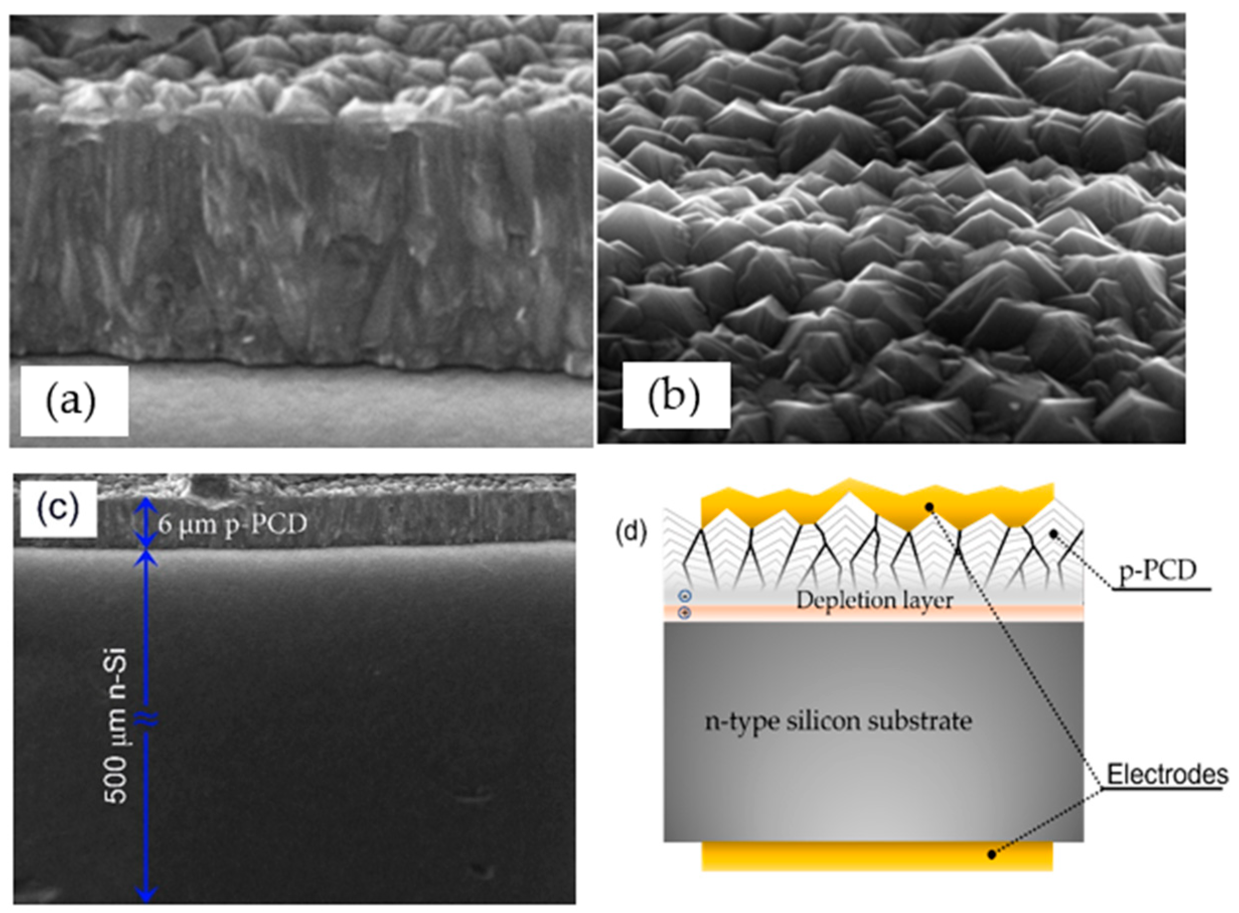
3.1. Surface Morphology Analysis

The SEM images of the studied diamond film are shown in Figure 1. At the bottom of the cross-section of diamond (Figure 1a), one can notice that there are distinct individual nanocrystallites that function as nucleation centers. After the nucleation stage, diamonds start to grow in the vertical direction along the fastest growing planes prevalent among the crystals. The resultant as-grown surface has remarkably high roughness due to the difference in heights of the growing columns, Figure 1b. The surface morphology shows an octahedral character. The cross section shown in Figure 1c discloses the PCD layer thickness and substrate as well. The scheme of the developed device is presented in Figure 1d.

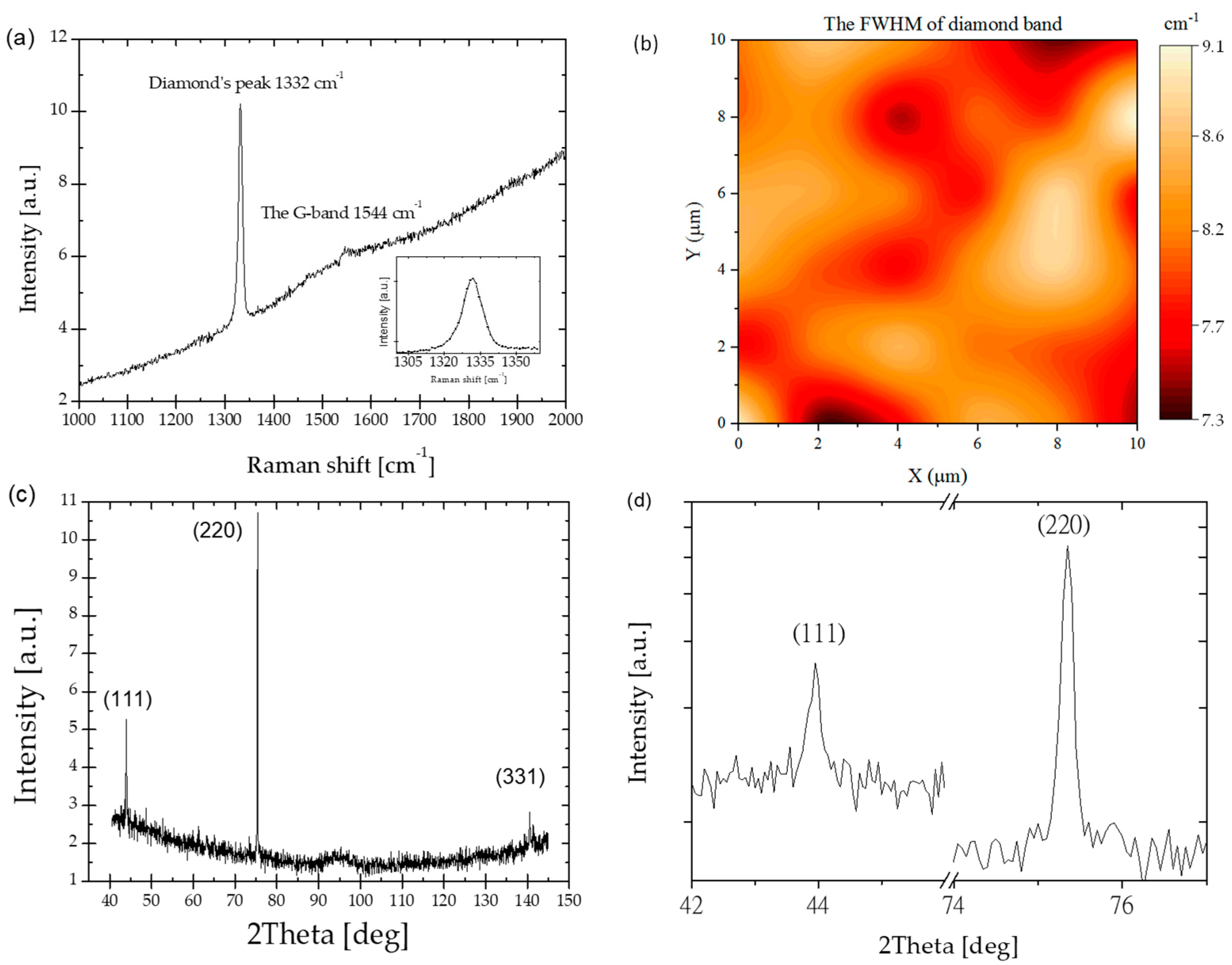
3.2. Raman Spectroscopy and XRD

The Raman and XRD spectra of the diamond layer are shown in Figure 2. Figure 2a shows a strong diamond line peaked at 1332 cm−1, i.e., close to the theoretical value for the sp3-hybridized diamond carbon phase. The full width at half of the maximum (FWHM) for a well-crystallized diamond sample is 7.8 cm−1. This is an indication of the excellent quality of the diamond layer. Figure 2b shows the Raman’s map of the FWHM on an area of 100 µm2. There is a generally accepted convention that the value of the FWHM greater than 12 cm−1 means a poor quality diamond, and a value lower than 12 cm−1 of a diamond layer is considered good quality [16]. The Raman spectrum displays also a broad band peaked at 1544 cm−1 corresponding to the non-diamond carbon form with the predominant sp2-hybridization. As can be seen from Figure 2a, the Raman lines are superimposed on a broad luminescent background, indicating that the diamond layer is hydrogenated. The hydrogen in diamond layers is responsible for its p-type surface conductivity [17]. The purity of the diamond layers was estimated according to the procedure described in our earlier paper [18] and was equal to 98.8%. It means that diamond quality is superb because the sp2 admixture is below 1.2%.
The final morphology of the PCD layer depends on the preferential growth direction of microcrystals in the diamond layers. It is known that in different crystallographic orientations, the density of defects generated during the growth process depends on the growth direction [19]. The XRD diffraction pattern shows three main reflections from (111), (220), and (331) crystal planes. The diffraction patterns were compared with the JCPDS No. 6-0675 file. As can be seen in Figure 2d, the diffraction peaks are narrow. The FWHM is lower than 0.15 degrees. This confirms the good quality of the diamond layers. The texture analysis allows us to estimate the texture coefficients, which are as follows: 6%, 81.3%, and 12.7%, respectively, for Tc(111) Tc(220), and Tc(331). It means that our diamond layers have (220) preferential orientation.

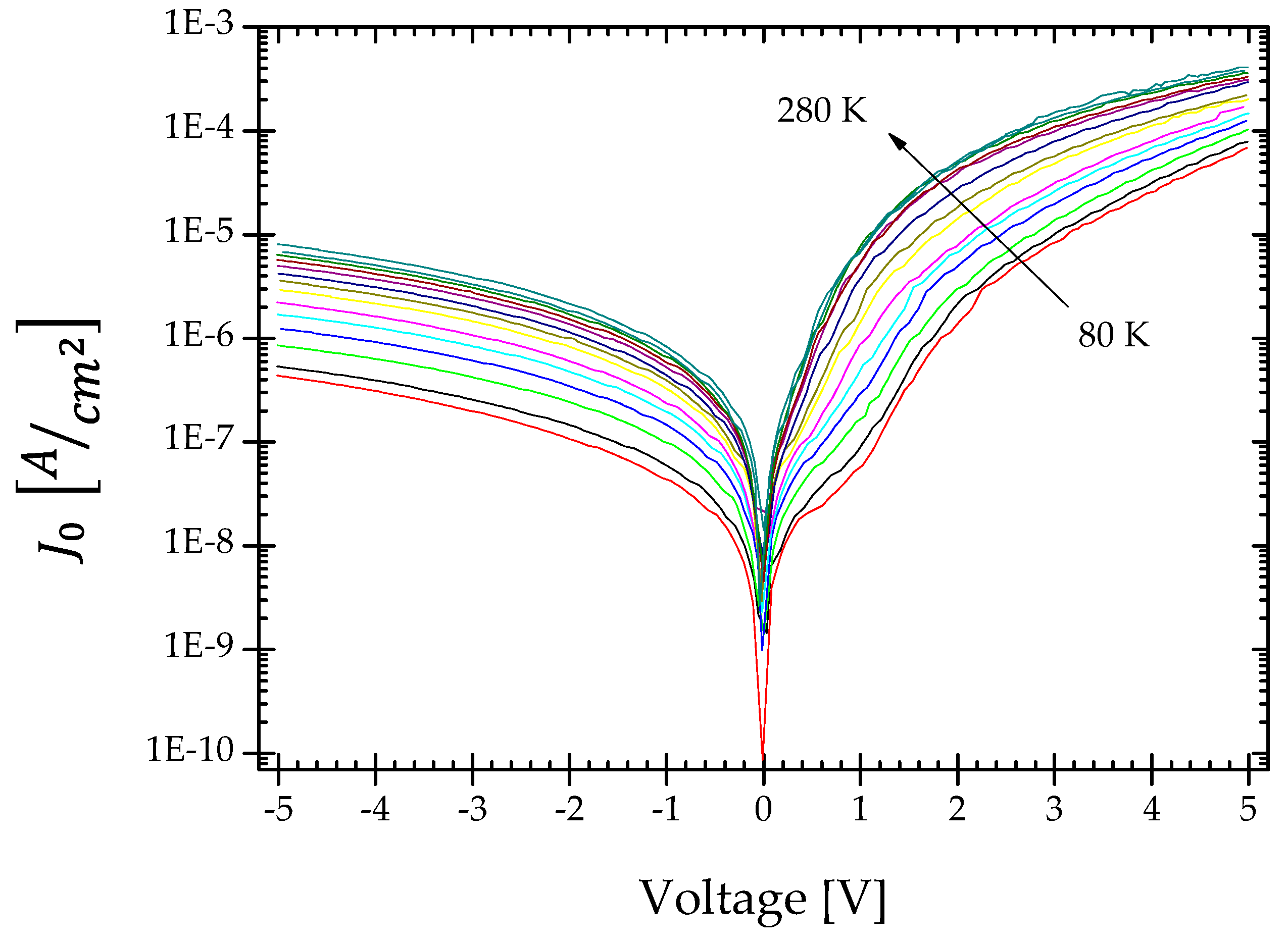
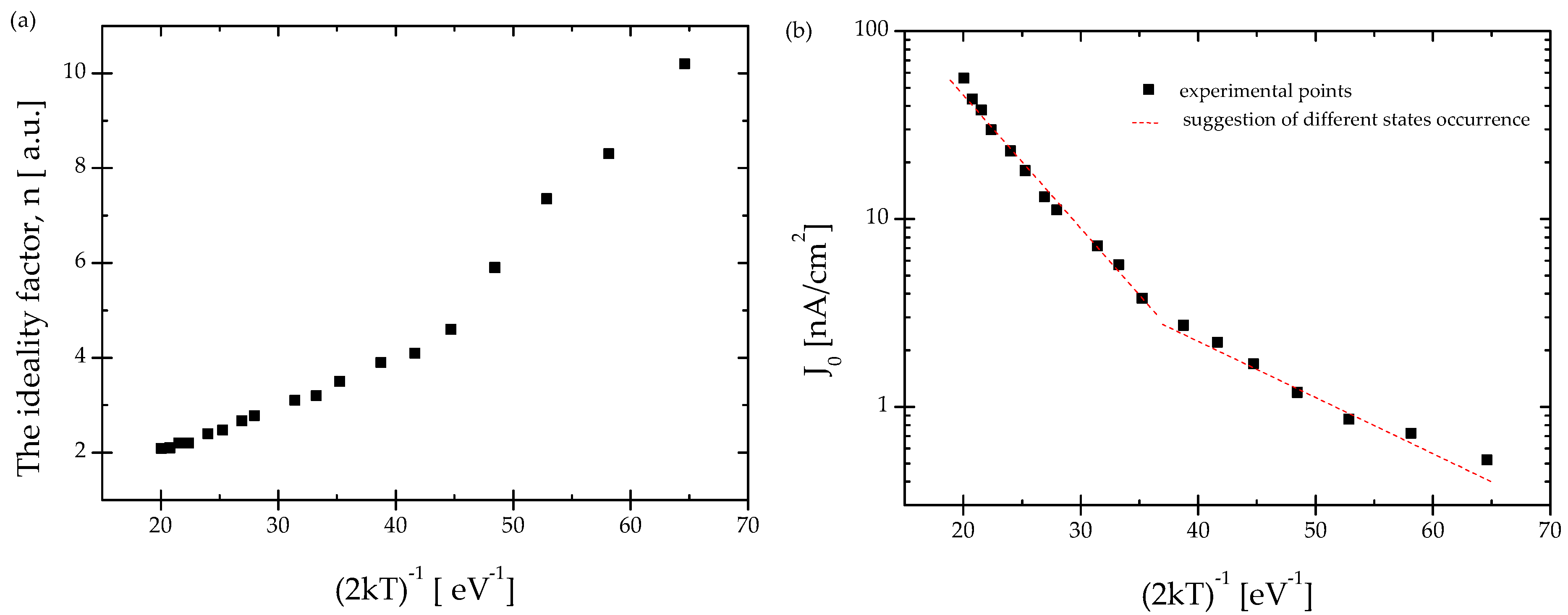
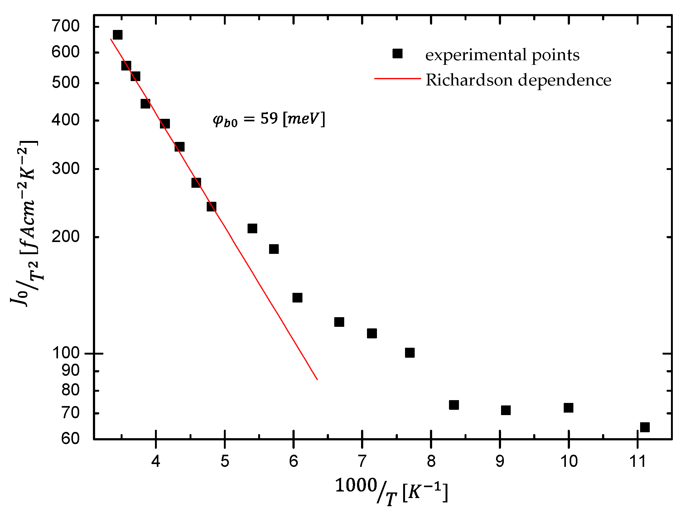
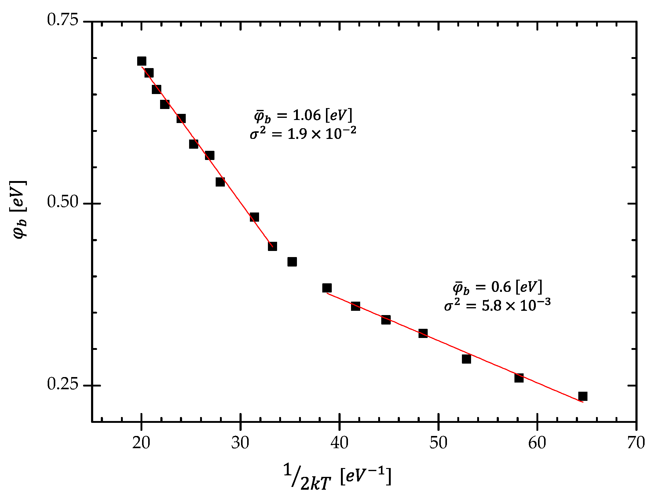
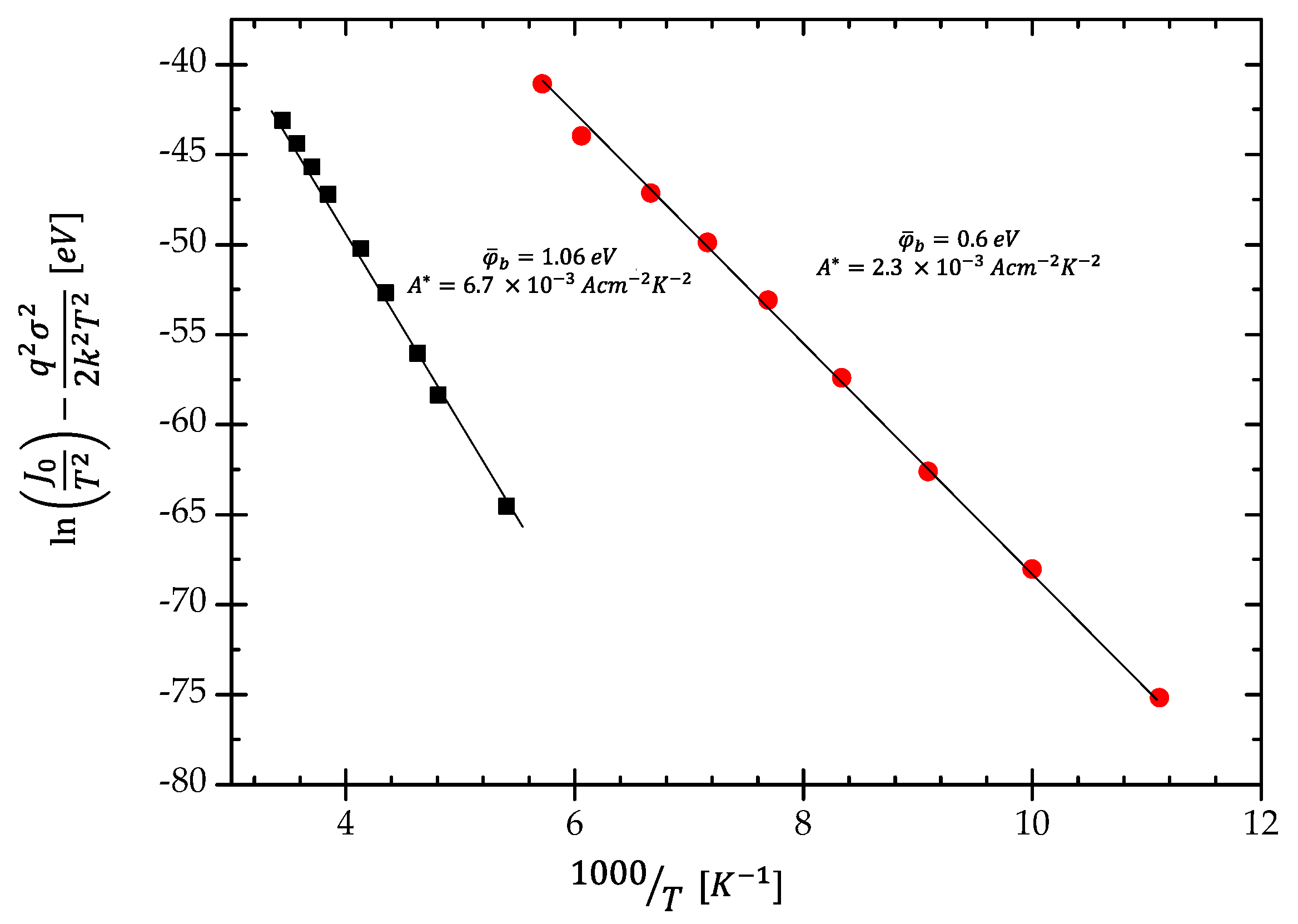
3.3. Diodes Characteristics

The I-V characteristics of the p-PCD/n-Si heterojunction were measured in the temperature range from 80 to 280 K. They are shown in Figure 3. At 280 K, the heterojunctions showed a rectifying character. The rectification ratio is approximately about two orders of magnitude at bias voltages of ±3 V, and confirms that a p-n diode is formed at the interface of the p-PCD/n-Si. According to the TE theory, the forward current is a function of the voltage and temperature according to the equation
J = A * T 2 exp ( q φ b k T ) [ e x p ( q V n k T ) 1 ] ,
This equation can be simplified by removing the term (−1) which is justified when V 3   kT / q , i.e., for V in the range of 0.1–0.4 V, which gives [20]
J = J 0 [ e x p ( q V n k T ) ]
where A * is the Richardson constant, T is the temperature, q is the electronic charge, φ b is the effective barrier height, k is the Boltzmann constant, V is the bias, and n is the ideality factor (for the ideal device n = 1), which is a dimensionless value. From the linear part of the plot of ln(J)–V usually in the range of 0–0.4 V, one can estimate the saturation current J 0 and the ideality factor n ,
n = q k T d V d ( l n J )
The value of the ideality coefficient is usually greater than one and may reach values even greater than 20 [21]. This is attributed to the presence of structural defects in the interfacial part of the heterojunction or series resistance, which influence the charges localization effect. Higher values reflect how much the energy of the biasing electric field has to be reduced in comparison to the thermal energy. However, a good and important explanation can be barrier inhomogeneities as well [22]. In particular, the large ideality factors already attracted attention very early [23,24] and are still being discussed. Previous explanations of high ideality factor values were based on trap-assisted tunneling or field-enhanced recombination via isolated point defect levels [25].
The ideality factor and saturation current versus inverse temperature are shown in Figure 4a,b, respectively. As it is seen the ideality factor, n increases with decreasing temperature, while the reverse saturation current decreases. It is generally assumed that if the n is equal to one, the carriers freely cross the junction using the thermal diffusion process [26]. However, at a lower temperature, the process can be disturbed by the stronger localization effect on the defects, and this is reflected by the n rise. Figure 4b clearly shows the existence of two different values of the slopes of the graph J 0 vs. 1/2 kT in the range of lower (80–170 K) and higher (170–280 K) temperatures. This may indicate the occurrence of at least two types of interface states in the heterojunction [27].
The saturation current, J0(T) is given by the formula [26,28]:
J 0 = A * T 2 exp ( φ b k T ) .
From the slope of Richardson’s plot, i.e., versus 1000/T presented in Figure 5, one can estimate the so-called zero-bias barrier height φb0. As seen, the plot reveals behavior that the entire range of measured temperatures can be divided into two different regions: linear in higher temperature ranges and region where the dependence deviates from linearity assumed by the TE theory. Such discrepancy is associated with the potential barriers’ inhomogeneities. The interface is not atomically flat but rough, with the result of spatial fluctuations. Thus, it cannot be described by classical TE theory assuming the existence of a single potential barrier. However, it can be explained by the model proposed by Werner et al. [11]. The deviation of the Richardson plot from linearity indicates the temperature dependence of the BH and its inhomogeneity caused by potential fluctuations at the interface [29,30,31].
Solving Equation (4), the barrier heights can be derived from the relation [30]:
φ b = k T q l n ( A * T 2 J 0 ) .
The calculated values of φb as a function of 1/2 kT are presented in Figure 6. The observed relation suggests the existence of two different barrier height distributions [32]. The increase in φb, with the temperature rise, is related to the presence of trap states in the interfacial layer. Due to the negative value of electrons’ affinity for the diamond structure [31], thermally emitted charges from the n-Si surface create a depletion layer with higher potential. According to Sullivan et al. [33], the barriers consist of laterally inhomogeneous patches of different barrier heights. The patches with lower barrier height yield a larger ideality factor and vice versa. There is indicated the temperature dependence of a density of interface states [6]. The inhomogeneity due to potential fluctuations can be described using the Gaussian distribution function of the barrier height around an average value. Hence, the total saturation current J 0 can be expressed by the formula [13]
J 0 = A * T 2 0 A ( φ b ) exp ( q φ b k T ) d φ b
where A ( φ b ) is a distribution function that describes the Schottky barrier inhomogeneities. Taking into account that the barrier variability can be approximated with two lines, in Figure 6, the distribution function can be assumed to be the sum of two Gaussians as is described in the following relation:
A ( φ b ) = A 1 σ 1 2 π e x p [ ( φ b φ ¯ b 1 ) 2 2 σ 1 2 ] + A 2 σ 2 2 π e x p [ ( φ b φ ¯ b 2 ) 2 2 σ 2 2 ] .
The parameters φ ¯ b i and σ i 2 (i = 1,2) of distribution functions can be obtained using the formula [22]
φ b = φ ¯ b i q σ i 2 2 k T .
The plot of φ b shown in Figure 6 allows estimating two parameters of the distribution function, average values φ ¯ b i of the BH and the standard deviation σi. They are as follows: BHs 0.6 eV and 1.06 eV and σ 0.0762 eV and 0.43 eV for lower 80 K–170 K and higher 170 K–280 K temperature ranges, respectively. The good fit of the experimental points by straight lines presented in Figure 6 confirms the hypothesis of the DGD of potential BHs.
Combining Equations (4) and (8), we obtain
ln ( J 0 T 2 ) q 2 σ i 2 2 k 2 T 2 = l n ( A A * ) φ ¯ b i k T .
This equation called the modified Richardson’s relation allows the estimation of the Richardson’s constant A* and amplitudes of the double Gaussian distribution function as well. Its plot versus inverse temperature produces again the straight line with the slope of the average barrier’s height. Yet, the intercept at the ordinate designates the A* value. Using Equation (9) to both temperature ranges gives the A* as 6.7 × 10⁻³ A cm−2 K−2 and 2.3 × 10⁻³ A cm−2 K−2, respectively, to higher and lower temperature ranges. Results are shown in Figure 7. Two different values of the Richardson constants result from the fact that, depending on the temperature range, we have two different Gaussian barrier potential distributions. The obtained values of Richardson’s constants are much smaller than the theoretical one of 90 A cm−2 K−2 [34]. The values of the Richardson’s constants reported in the literature [4,35,36,37] are in the wide range of 1.0995–1.9 × 10⁻⁹ A cm−2 K−2. To date, the problem of the measured Richardson’s constant values for several types of junctions has not been properly explained. However, to obtain a good fit, the Gaussian amplitudes need to be arbitrarily chosen. They undergo the normalization condition A1(φb1) + A2(φb2) = 1. Finally, estimated values are 0.64 and 0.36, respectively, for both Gaussian functions at higher and lower temperature ranges.
Based on the research carried out, it can be said that the ideality factor increases with the temperature decrease, while the height of the potential barrier decreases. At the higher temperature range, where the n is close to one, charges are subjected to a thermally diffusive process with a higher value of average potential and emission Richardson’s constant as well. A gradual temperature decrease results in parameter change, presumably due to the charges localization effect at interstitial defects. In the case of this study, it was found a 170 K temperature for the abrupt parameters change. Below and above this temperature, the averaging needs to be calculated around other values due to the impact of the stronger influence of the localization effect at lower temperatures. Localized charges have an influence on each aspect of current carriers’ transport through the heterojunction: the ideality factor, barrier’s height, and barrier homogeneity, as well as the series resistance Rs [6,7].

4. Conclusions

In the present work, the heterojunctions of p-type PCD/n-Si were developed. PCD film was grown by the HF CVD method, while the n-type Si substrate is a commercially available single crystal. The structural properties of the diamond layer were characterized by SEM, Raman spectroscopy, and XRD. The J-V-T characteristics were measured in the temperature range of 80–280 K. From the J-V-T curves, the junction parameters, i.e., the ideality factor n and the height of the potential barrier φ b , were computed using the TE theory. Through the TE theory, the value for the n varies from 2.7 at 280 K to 8.7 at 80 K, while φ b increases with temperature. Due to the assumed inhomogeneity of the heights of the potential barriers, the range of the temperature changes was divided into two ranges. The obtained average values of φ ¯ b in lower 80 K–170 K, and higher 170 K–280 K temperature ranges are 0.6 eV and 1.06 eV, respectively. The averaging was performed by the double Gaussian distribution function. Its parameters are as follows: amplitudes of 0.64 and 0.36 and standard deviations of 0.43 eV and 0.0762 eV, respectively, to higher and lower temperature ranges. This procedure allows the linearization of the modified Richardson’s relation and the estimation of Richardson’s constant A*. They take values of 6.7 × 10⁻³ A cm−2 K−2 and 2.3 × 10⁻³ A cm−2 K−2, respectively, to higher and lower temperature ranges. In our opinion, the division in two temperature ranges is caused by the charge localization influence on interfacial defects. This effect is stronger at lower temperatures.

Author Contributions

Conceptualization, S.Ł. and K.F.; Data curation, K.P.; Formal analysis, S.Ł. T.K., and A.D.; Funding acquisition, S.Ł., K.P., W.K. and M.S.; Investigation, W.K., T.K., S.Ł., K.P. and A.D.; Methodology, K.F.; Project administration, S.Ł. and K.F.; Resources, K.P.; Software, S.Ł.; Supervision, K.F.; Validation, S.Ł., K.F., K.P. and M.S.; Visualization, W.K. and T.K.; Writing—original draft, K.F.; Writing—review & editing, S.Ł. and M.S. All authors have read and agreed to the published version of the manuscript.

Funding

The research received no external funding.

Institutional Review Board Statement

Not applicable.

Informed Consent Statement

Not applicable.

Data Availability Statement

Data are not available.

Conflicts of Interest

The authors declare no conflict of interest.

References

  1. Wort, C.J.; Balmer, R.S. Diamond as an electronic material. Mater. Today 2008, 11, 22–28. [Google Scholar] [CrossRef]
  2. Denisenko, A.; Kohn, E. Diamond power devices. Concepts and limits. Diam. Relat. Mater. 2005, 14, 491–498. [Google Scholar] [CrossRef]
  3. Kohn, E.; Denisenko, A. Concepts for diamond electronics. Thin Solid Films 2007, 515, 4333–4339. [Google Scholar] [CrossRef]
  4. Traoré, A.; Muret, P.; Fiori, A.; Eon, D.; Gheeraert, E.; Pernot, J. Zr/oxidized diamond interface for high power Schottky diodes. Appl. Phys. Lett. 2014, 104, 052105. [Google Scholar] [CrossRef]
  5. Umezawa, H.; Saito, T.; Tokuda, N.; Ogura, M.; Ri, S.-G.; Yoshikawa, H.; Shikata, S.-I. Leakage current analysis of diamond Schottky barrier diode. Appl. Phys. Lett. 2007, 90, 073506. [Google Scholar] [CrossRef]
  6. Łoś, S.; Fabisiak, K.; Paprocki, K.; Szybowicz, M.; Dychalska, A. The Undoped Polycrystalline Diamond Film—Electrical Transport Properties. Sensors 2021, 21, 6113. [Google Scholar] [CrossRef]
  7. Łoś, S.; Fabisiak, K.; Paprocki, K.; Szybowicz, M.; Dychalska, A.; Spychaj-Fabisiak, E.; Franków, W. The hydrogenation impact on electronic properties of p-diamond/n-si heterojunctions. Materials 2021, 14, 6615. [Google Scholar] [CrossRef]
  8. Łoś, S.; Paprocki, K.; Fabisiak, K.; Szybowicz, M. The influence of the space charge on The Ohm’s law conservation in CVD diamond layers. Carbon 2019, 143, 413–418. [Google Scholar] [CrossRef]
  9. Hayashi, K.; Yamanaka, S.; Okushi, H.; Kajimura, K. Study of the effect of hydrogen on transport properties in chemical vapor deposited diamond films by Hall measurements. Appl. Phys. Lett. 1998, 68, 376. [Google Scholar] [CrossRef]
  10. Baumann, P.K.; Nemanich, R.J. Electron affinity and Schottky barrier height of metal–diamond (100), (111), and (110) interfaces. J. Appl. Phys. 1998, 83, 2072. [Google Scholar] [CrossRef]
  11. Werner, J.H.; Güttler, H.H. Barrier inhomogeneities at Schottky contacts. J. Appl. Phys. 1991, 69, 1522–1533. [Google Scholar] [CrossRef]
  12. Iucolano, F.; Roccaforte, F.; Giannazzo, F.; Raineri, V. Barrier inhomogeneity and electrical properties of Pt∕GaN Schottky contacts. J. Appl. Phys. 2007, 102, 113701. [Google Scholar] [CrossRef]
  13. Güçlü, Ç.; Özdemir, A.F.; Altindal, Ş. Double exponential I–V characteristics and double Gaussian distribution of barrier heights in (Au/Ti)/Al2O3/n-GaAs (MIS)-type Schottky barrier diodes in wide temperature range. Appl. Phys. A Mater. Sci. Process. 2016, 122, 1032. [Google Scholar] [CrossRef]
  14. Tataroǧlu, A.; Altindal, Ş. The distribution of barrier heights in MIS type Schottky diodes from current–voltage–temperature (I–V–T) measurements. J. Alloys Compd. 2009, 479, 893–897. [Google Scholar] [CrossRef]
  15. Fiat, S.; Merdan, Z.; Memmedli, T. Current-conduction mechanisms in Au/n-CdTe Schottky solar cells in the wide temperature range. Phys. B Condens. Matter 2012, 407, 2560–2565. [Google Scholar] [CrossRef]
  16. Mallik, A.K.; Dandapat, N.; Chakraborty, S.; Mandal, A.K.; Ghosh, J.; Unnikrishnan, M.; Bysakh, S.; Balla, V. Characterizations of microwave plasma CVD grown polycrystalline diamond coatings for advanced technological applications. Process. Appl. Ceram. 2014, 8, 69–80. [Google Scholar] [CrossRef]
  17. Iacobucci, S.; Alippi, P.; Calvani, P.; Girolami, M.; Offi, F.; Petaccia, L.; Trucchi, D.M. Electronic structure of hydrogenated diamond: Microscopical insight into surface conductivity. Phys. Rev. B 2016, 94, 045307. [Google Scholar] [CrossRef]
  18. Paprocki, K.; Dittmar-Wituski, A.; Trzcinski, M.; Szybowicz, M.; Fabisiak, K.; Dychalska, A. The comparative studies of HF CVD diamond films by Raman and XPS spectroscopies. Opt. Mater. 2019, 95, 109251. [Google Scholar] [CrossRef]
  19. Butler, J.E.; Oleynik, I. A mechanism for crystal twinning in the growth of diamond by chemical vapour deposition. Philos. Trans. R. Soc. A Math. Phys. Eng. Sci. 2007, 366, 295–311. [Google Scholar] [CrossRef]
  20. Rajpalke, M.K.; Bhat, T.N.; Roul, B.; Kumar, M.; Krupanidhi, S.B. Current transport in nonpolar a-plane InN/GaN heterostructures Schottky junction. J. Appl. Phys. 2012, 112, 023706. [Google Scholar] [CrossRef]
  21. Belgacem, C.H.; El-Amine, A.A. Theoretical Models for Anomalously High Ideality Factor in a Au/SnO 2-Si(n)/Al Solar Cell. Silicon 2018, 10, 1063–1066. [Google Scholar] [CrossRef]
  22. Aydoǧan, Ş.; Saǧlam, M.; Türüt, A. On the barrier inhomogeneities of polyaniline/p-Si/Al structure at low temperature. Appl. Surf. Sci. 2005, 250, 43–49. [Google Scholar] [CrossRef]
  23. Riben, A.R.; Feucht, D.L. nGe/pGaAs Heterojunctions. Solid-State Electron. 1966, 9, 1055–1065. [Google Scholar] [CrossRef]
  24. Queisser, H.J. Forward characteristics and efficiencies of silicon solar cells. Solid-State Electron. 1962, 5, 1–10. [Google Scholar] [CrossRef]
  25. Kaminski, A.; Marchand, J.J.; Omari, Q.N.; el Laugier, H.; Le, A.; Sarti, D. Conduction processes in silicon solar cells. In Proceedings of the Conference Record of the Twenty Fifth IEEE Photovoltaic Specialists Conference-1996, Washington, DC, USA, 13–17 May 1996; pp. 573–576. [Google Scholar]
  26. Chaleawpong, R.; Promros, N.; Charoenyuenyao, P.; Hanada, T.; Ohmagari, S.; Zkria, A.; Yoshitake, T. Diode Parameters of Heterojunctions Comprising p-Type Ultrananocrystalline Diamond Films and n-Type Si Substrates. J. Nanosci. Nanotechnol. 2019, 19, 1567–1573. [Google Scholar] [CrossRef] [PubMed]
  27. Promros, N.; Chen, L.; Yoshitake, T. Near-infrared photodetection in n-type nanocrystalline FeSi 2/p-type Si heterojunctions. J. Nanosci. Nanotechnol. 2013, 13, 3577–3581. [Google Scholar] [CrossRef] [PubMed]
  28. Cheung, S.K.; Cheung, N.W. Extraction of Schottky diode parameters from forward current-voltage characteristics. Appl. Phys. Lett. 1998, 49, 85. [Google Scholar] [CrossRef]
  29. Horváth, Z.J. Comment on ‘analysis of I-V measurements on CrSi2-Si Schottky structures in a wide temperature range’. Solid-State Electron. 1996, 39, 176–178. [Google Scholar] [CrossRef]
  30. Jabbari, I.; Baira, M.; Maaref, H.; Mghaieth, R. Schottky barrier inhomogeneity in (Pd/Au) Al0.22 Ga0.78N/GaN/SiC HEMT: Triple Gaussian distributions. Chin. J. Phys. 2021, 73, 719–731. [Google Scholar] [CrossRef]
  31. Crawford, K.G.; Maini, I.; Macdonald, D.A.; Moran, D.A.J. Surface transfer doping of diamond: A review. Prog. Surf. Sci. 2021, 96, 100613. [Google Scholar] [CrossRef]
  32. Mohan, L.; Chandan, G.; Mukundan, S.; Roul, B.; Krupanidhi, S.B. Double Gaussian distribution of barrier height observed in densely packed GaN nanorods over Si (111) heterostructures. J. Appl. Phys. 2014, 116, 234508. [Google Scholar] [CrossRef]
  33. Sullivan, J.P.; Tung, R.T.; Pinto, M.R.; Graham, W.R. Electron transport of inhomogeneous Schottky barriers: A numerical study. J. Appl. Phys. 1998, 70, 7403. [Google Scholar] [CrossRef]
  34. Malakoutian, M.; Benipal, M.; Koeck, F.A.; Nemanich, R.J.; Chowdhury, S. Schottky Barrier Height Analysis of Diamond SPIND Using High Temperature Operation up to 873 K. IEEE J. Electron Devices Soc. 2020, 8, 614–618. [Google Scholar] [CrossRef]
  35. Ueda, K.; Kawamoto, K.; Asano, H. High-temperature and high-voltage characteristics of Cu/diamond Schottky diodes. Diam. Relat. Mater. 2015, 57, 28–31. [Google Scholar] [CrossRef]
  36. Suzuki, M.; Koizumi, S.; Katagiri, M.; Ono, T.; Sakuma, N.; Yoshida, H.; Sakai, T.; Uchikoga, S. Electrical characteristics of n-type diamond Schottky diodes and metal/diamond interfaces. Phys. Status Solidi 2006, 203, 3128–3135. [Google Scholar] [CrossRef]
  37. Vescan, A.; Daumiller, I.; Gluche, P.; Ebert, W.; Kohn, E. Very high temperature operation of diamond Schottky diode. IEEE Electron Device Lett. 1997, 18, 556–558. [Google Scholar] [CrossRef]
Figure 1. SEM images analysis of (a) cross-section of the diamond layer, (b) the surface morphology, (c) cross section of p-PCD/n-Si heterojunction, and (d) a two-dimensional schematic cross section of the heterojunction.
Materials 15 05895 g001
Figure 2. The structural analysis of diamond layers, (a) the Raman spectrum, in the insert, details of the diamond peak, (b) Raman’s mapping of the FWHM, (c) XRD diffractogram of the investigated diamond, and (d) details of the two most prominent diffraction peaks.
Materials 15 05895 g002
Figure 3. I-V-T characteristics of p-PCD/n-Si heterojunction.
Materials 15 05895 g003
Figure 4. The temperature dependence of the experimental (a) ideality factor n , and (b) the reverse saturation current of the diode for Au/p-PCD/n-Si/Au structure.
Materials 15 05895 g004
Figure 5. The conventional Richardson’s plot.
Materials 15 05895 g005
Figure 6. The variation of the barrier height φ b as a function of (1/2 kT) according to the Werner model.
Materials 15 05895 g006
Figure 7. The modified Richardson’s plot.
Materials 15 05895 g007
Publisher’s Note: MDPI stays neutral with regard to jurisdictional claims in published maps and institutional affiliations.

