Abstract
Honeycomb sandwich structures (HSSs) are excellent candidates for light and efficient microwave-absorbing materials. In this work, we design an HSS using SiO2 fiber-reinforced epoxy resin (SiO2f/ER) composites as both the top and bottom layers to improve the impedance matching with free space. Target dielectric properties of the honeycomb and coated lossy material of the HSS were calculated based on the multilayer transmission line theory, metal backplane model, and homogenization theory. In addition, the interface effect between the SiO2f/ER and honeycomb of the HSS was discussed theoretically, experimentally, and numerically, indicating a 1–4% contribution of microwave absorption resulting from the interface. By analyzing the equivalent resistance, equivalent capacitance, as well as equivalent inductance, the enhanced microwave absorption of HSS is attributed to the formation of the interfacial transition zone, which benefits both impedance matching and electromagnetic loss.
1. Introduction
The offensive and defensive battles of radar and stealth aircraft are constantly being staged on the modern information battlefield, originating from the second world war [1,2]. The first generation of radar-absorbing materials, represented by ferrite-based coatings, was manufactured by the Germans in response to the early radar devices successfully developed by the Allies. Therefore, the rapid development of radar detection technology promoted the design of a new generation of absorbing materials/structures [3,4,5,6].
Aramid honeycomb sandwich structure (AHSS) has relatively low dielectric constant and dielectric loss, and thus exhibits excellent microwave transmission properties when quartz fiber-reinforced resin is used as top and bottom panels to ensure the detection range and strike accuracy of the radar [7]. AHSS also exhibits excellent microwave absorption properties when conductive coatings such as carbon nanotube, carbon black, conductive polymers, or magnetic powders are attached to the inner wall of the honeycomb to reduce the radar cross section (RCS) [8,9,10,11,12]. At the same time, the high flexural strength/mass ratio and strong anti-instability ability of AHSS determine that it plays an important structural and functional integration role of “wave-transmitting spear and stealth shield” on stealth aircraft [13,14,15]. In addition to the mesoscopic scale design of AHSS, the microstructure design of conductive fillers can also serve as an important means to improve electromagnetic absorption and shielding capabilities [16,17].
According to the literature, many researchers have explored the effect of the honeycomb structure size, thickness, and electrical properties of coated lossy material, as well as panel matching layer thickness, on microwave absorption efficiency thanks to the excellent design-ability of the honeycomb sandwich structure [18,19]. At the same time, a frequency selective surface is designed and introduced into AHSS to achieve broadband tunable microwave absorbing properties [20]. The interface between the panel matching layer and the honeycomb produces an interface polarization effect in the alternating electromagnetic field, which is known as the Maxwell–Wagner–Sillars (MWS) effect, and can also consume microwave energy [21,22,23,24]. However, the MWS effect between the panel matching layer and honeycomb has not yet been discussed and quantified.
In this paper, the honeycomb sandwich structure with SiO2f/ER as matching panels based on the design principle of multilayer transmission line theory and the metal backplane model is proposed theoretically, experimentally, and numerically to quantify the role of the interface effect. The respective impedance, resistance, capacitance, and inductance, both when considering the interface effect and not considering the interface effect, are calculated and used to further analyze the underlying mechanism of electromagnetic loss at the interface.
2. Experimental and Simulation Method
2.1. Material Fabrication
Figure 1 shows the schematic of a unit cell in the designed honeycomb sandwich structure. Firstly, the SiO2f/ER layer with a thickness d1 of 1.5 mm serving as the panel matching layer was prepared by the vacuum pressure impregnation process, in which the mass fraction of epoxy resin is 35% and the corresponding dielectric constant ε = 3.4 (1-j0.025) at 10 GHz. Secondly, the conductive coating with a thickness d of 0.15 mm was prepared using a high-speed mixer. Here, the mass fraction of conductive carbon black powders (Nanjing Xianfeng Chemical Co., Ltd., Nanjing, China) is 28% and the corresponding mass fraction of epoxy resin is 72%. Thirdly, a conductive coating was introduced into inner wall of honeycomb via the dip-coating process; here, the dipping time is 1 min, following by drying in a blast drying oven at 90 °C for 10 min. By repeating the dip-coating process on the opposite face to the previous time, the uniformity of the coating thickness along the honeycomb height direction is ensured and the coating thickness can be calculated based on the honeycomb weight gain. Fourthly, the panel and honeycomb are bonded by adhesive film, whose thickness is 0.2 mm and with the corresponding dielectric constant ε = 3.5 (1-j0.02) at 10 GHz, which can be studied together with the panel.
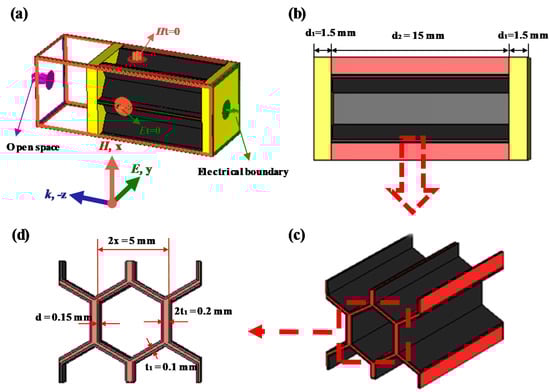
Figure 1.
Schematic of a unit cell in the designed honeycomb sandwich structure: (a) 3D view, (b) side view, (c) honeycomb core, and (d) geometry of the honeycomb core.
2.2. Characterization, Simulation, and Calculation
The respective dielectric properties of the conductive coating and the corresponding honeycomb core were determined by a vector network analyzer (VNA, MS4644A; Anritsu, Atsugi, Japan) in X-band (8.2–12.4 GHz), using a 22.86 mm × 10.16 mm rectangular waveguide. The reflection loss experimental results in X-band of the fabricated honeycomb sandwich structure with dimensions of 180 mm × 180 mm × 18 mm were measured using the free space method. CST Microwave Studio was used to perform numerical simulation on the honeycomb sandwich structure based on the finite integration technique.
Three-layer transmission line theory and the metal backplane model were used to calculate the reflection loss (RL), impedance, and corresponding microwave absorption efficiency (A()) of the honeycomb sandwich structure, which can be expressed as follows [25,26]:
where Zi is the normalized impedance (the ratio of complex impedance to vacuum impedance) of layer i from the bottom up; εi and di are the relative complex permittivity (the ratio of complex permittivity to vacuum permittivity) and thickness of layer i, respectively; f is the frequency of microwave; c represents the speed of light in the free space; and is the angular frequency of microwave.
3. Results and Discussion
3.1. Target Dielectric Properties of the Honeycomb and Coated Lossy Material
For the three-layer absorbing structure in this work, the target equivalent dielectric properties of the honeycomb core 15 mm in height can be calculated according to Equations (1)–(4) when the thickness of the top and bottom panels is 1.5 mm and the corresponding dielectric constant ε = 3.4 (1-j0.025) at 10 GHz. Figure 2 exhibits the contour plot of RL corresponding to different dielectric properties of the honeycomb core at 8.2 GHz, 9.2 GHz, 10.2 GHz, 11.2 GHz, and 12.2 GHz, respectively. The bold purple circle in Figure 2 shows the range where RL is less than −10 dB. It can be concluded that lower equivalent dielectric properties of the honeycomb can significantly increase the target range of equivalent dielectric properties.
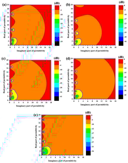
Figure 2.
Reflection loss spectrums of a honeycomb core 15 mm in height with different equivalent dielectric properties: (a) 8.2 GHz, (b) 9.2 GHz, (c) 10.2 GHz, (d) 11.2 GHz, and (e) 12.2 GHz.
Based on the strong interference theory and long-wave approximation, the equivalent dielectric property of a honeycomb εz 15 mm in height can be expressed as follows [27]:
where ε1 and ε2 are the relative complex permittivity of coated lossy material and the aramid fiber, respectively, where ε2 = 2 (1-j0.015) at 10 GHz; εz and εp are the equivalent relative complex permittivity of the honeycomb core and coated lossy material combined with its surrounding air column, respectively; t1 is the thickness of the aramid honeycomb core wall; and x represents half the distance between the opposite wall of the aramid honeycomb core.
Therefore, according to Equations (5) and (6), the target dielectric range of coated lossy material in Figure 3 can be obtained from the target equivalent dielectric range of the honeycomb core, which is shown in Figure 2. As shown in Figure 3, the existence of the high-porosity aramid honeycomb framework significantly increases the target dielectric range of the coated lossy material, which implies a more easily tunable microwave-absorbing performance.
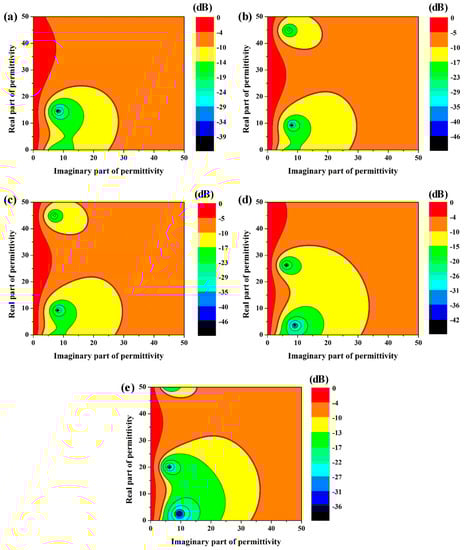
Figure 3.
Reflection loss spectrums of the coated lossy material with different dielectric properties: (a) 8.2 GHz, (b) 9.2 GHz, (c) 10.2 GHz, (d) 11.2 GHz, and (e) 12.2 GHz.
3.2. Microwave Absorption of the Honeycomb Sandwich Structure
In order to improve microwave absorption property of the honeycomb sandwich structure, a carbon black/ER composite with dielectric properties in the target range of coated lossy material obtained from Section 3.1 is introduced into the honeycomb inner wall with a coating thickness of 0.15 mm. The respective dielectric properties of the coated lossy material and corresponding honeycomb are shown in Figure 4a,b. It is obvious that the coated lossy material and corresponding honeycomb have a significant frequency dispersion effect, thus exhibiting a greater hysteresis effect of polarized charges and enhancing the loss of microwave energy. For dielectric lossy material in this work, the cole–cole diagram reflects its microwave loss mechanism. Specifically, one semicircle indicates one Debye polarization and relaxation process and one straight line indicates a conductive loss dominated loss mechanism. Figure 4c,d exhibits the respective cole–cole diagrams of the coated lossy material and corresponding honeycomb, which indicate a loss mechanism dominated by conductive loss.
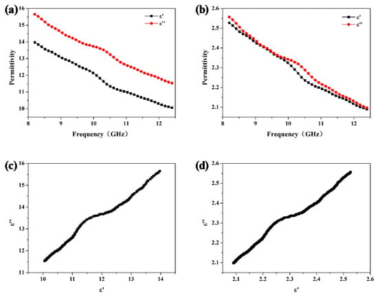
Figure 4.
Dielectric properties (a,b) and cole–cole diagram (c,d) of the coated lossy material and corresponding honeycomb.
Figure 5 exhibits the reflection loss and corresponding absorption efficiency of the honeycomb sandwich structure obtained from the impedance matching model according to Equations (1)–(4), as well as the CST simulation method and experiment. The CST simulation result and experimental result take into account the effect of the interface between the SiO2/ER panel and honeycomb in the sandwich structure. RL has a deviation of less than 1 dB in the X-band and the corresponding deviation of microwave absorption efficiency is less than 1%, verifying the accuracy of the simulation results. Interestingly, the impedance matching model calculation result when the interface effect between the SiO2/ER panel and honeycomb is not considered exhibits a relatively low reflection loss and poor microwave absorption efficiency. The presence of the interface between the panel and honeycomb reduces the RL by 1–4 dB in the X-band and the corresponding microwave absorption efficiency increased by 1%–4%, which implies that the interface plays an important role in the absorption of microwave energy. Next, we will further investigate the role of the interface effect from impedance, resistance, capacitance, and inductance with and without the interface effect.
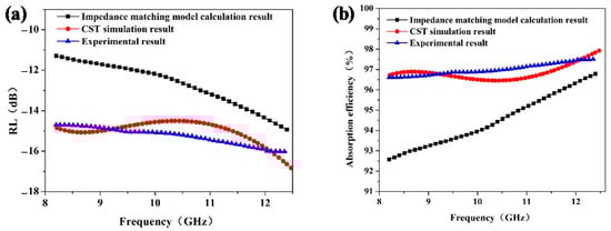
Figure 5.
Reflection loss (a) and corresponding microwave absorption efficiency (b) of the impedance matching model calculation result, CST simulation result, and experiment result.
3.3. Role of the Interface Effect
To further investigate the role of the interface effect in the honeycomb sandwich structure, respective normalized impedance of the CST simulation result and impedance matching model calculation result are exhibited in Figure 6. The real part of impedance represents the ability to dissipate energy from microwave and the imaginary part of impedance represents the ability to store microwave energy. When considering the interface effect, the CST simulation result exhibits a higher overall real part of impedance as well as a relatively lower imaginary part of impedance, which indicate excellent impedance matching performance. Interestingly, at the frequency point of 10 GHz, the interface has almost no effect on the real part of impedance, while it significantly reduces the imaginary part of impedance. This interesting phenomenon indicates that the presence of the interface reduces the ability to store charge and the interface acts as a charge transporter between the honeycomb and panel.
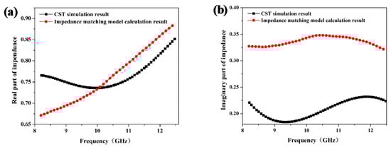
Figure 6.
Real (a) and imaginary (b) part of impedance obtained from the CST simulation result and impedance matching model result.
According to the structural characteristics of the honeycomb core and honeycomb sandwich structure, the respective equivalent circuit models are shown in Figure 7. Here, C1 represents the capacitance between opposing honeycomb walls; R1 and L1 represent the resistance and inductance, respectively; and C2 and C3 represent the capacitance of the upper and lower panel, respectively. According to the equivalent circuit, the impedance of the honeycomb sandwich structure can be expressed as follows:
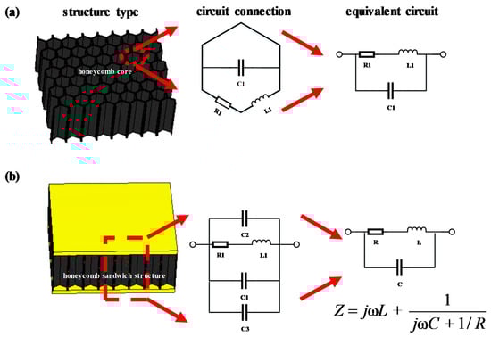
Figure 7.
Equivalent circuit model for the (a) honeycomb and (b) honeycomb sandwich structure.
According to Equation (7), the respective resistance, capacitance, and inductance can be obtained from the real and imaginary part of impedance represented in Figure 6. Specifically, the resistance, capacitance, and inductance at 10 GHz can be calculated from the values of the real and imaginary part of impedance at 9.99 GHz and 10.01 GHz when the changes in resistance, capacitance, and inductance caused by 0.02 GHz are considered negligible.
The corresponding calculation results at different frequency points in the X-band are shown in Figure 8. Obviously, the overall resistance, capacitance, and inductance decrease when considering the interface effect. The charge accumulated at the interface can easily migrate on both sides of the interface. Interestingly, the resistance, capacitance, and inductance show minimal values near 10 GHz, which means a more significant interface effect.
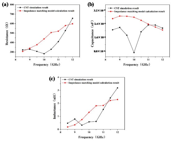
Figure 8.
Resistance (a), capacitance (b), and inductance (c) obtained from the CST simulation and impedance matching model.
Figure 9 demonstrates the distribution of the electric field energy density and magnetic field energy density at 10 GHz, which are analyzed to investigate the underlying physical mechanism of microwave absorption considering the interface effect. Here, the incident electromagnetic field is a uniform plane wave and the corresponding incident electric field energy density is 2 × 10⁻² J/m3. Compared with the microwave absorption without considering the interface effect, a strong coupling of the electric field and magnetic field emerges at the interface area of the panel and honeycomb. In particular, the energy concentration of electric and magnetic field occurs in both sides of the interface thin layer region. Thus, the existence of the interface transition zone, on one hand, improves the impedance matching and enables more microwave incident into the material. On the other hand, the increases in energy density of the electric field and magnetic field enhance the electromagnetic coupling effect and increase the loss of microwave energy. Therefore, the interface play an important role in the enhancement of microwave absorption efficiency in the honeycomb sandwich structure.
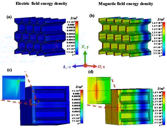
Figure 9.
Simulated distributions of electric field energy density (left) and magnetic field energy density (right) of microwave-absorbing structures: (a,b) honeycomb core; (c,d) honeycomb sandwich structure.
Furthermore, the power loss density distributions of the honeycomb sandwich structure and the corresponding honeycomb inside the sandwich structure are shown in Figure 10. The interface between the upper panel and honeycomb exhibits a strong electromagnetic loss, which is attributed to the strong electromagnetic coupling effect. Therefore, the existence of the interface transition zone reduces the overall resistance, capacitance, and inductance, which optimize impedance matching and enable more microwave incident into the material. At the same time, an enhanced electromagnetic coupling effect occurs in the interface transition zone, which improves the energy loss of microwave.
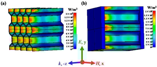
Figure 10.
Simulated distributions of the power loss density of the (a) honeycomb core and (b) honeycomb sandwich structure.
4. Conclusions
A honeycomb sandwich structure based on multilayer transmission line theory and the metal backplane model with enhanced microwave absorption is proposed in this paper. Theoretical, experimental, and numerical results indicate that the interface between the panel and honeycomb play a vital role in the loss of microwave energy, where the existence of the interface contributes 1–4% of microwave absorption efficiency in the X-band. On one hand, the existence of the interface significantly reduces the resistance, capacitance, and inductance and more microwave can incident into material. On the other hand, enhanced incident microwave exhibits a strong electromagnetic coupling phenomenon in the thin layer region near the interface and enhances the loss of microwave energy. Therefore, interface design can be used as a supplementary means to further optimize the microwave absorption efficiency of the honeycomb sandwich structure.
Author Contributions
Conceptualization, G.J.; Data curation, Y.Z. and Y.S. (Yungang Sun); Formal analysis, Y.Z.; Investigation, G.J. and M.L.; Software, W.S. and M.L.; Supervision, Y.S. (Yimeng Shan); Writing—original draft, Y.Z.; Writing—review & editing, Y.S. (Yimeng Shan). All authors have read and agreed to the published version of the manuscript.
Funding
This research received no external funding.
Institutional Review Board Statement
Not applicable.
Informed Consent Statement
Not applicable.
Data Availability Statement
All the data are available within the manuscript.
Conflicts of Interest
The authors declare no conflict of interest.
References
- Micheli, D.; Vricella, A.; Pastore, R.; Marchetti, M. Synthesis and electromagnetic characterization of frequency selective radar absorbing materials using carbon nanopowders. Carbon 2014, 77, 756–774. [Google Scholar] [CrossRef]
- Sheffield, R.G. Official F-19 Stealth Fighter Handbook; Compute Pu: Berlin/Heidelberg, Germany, 1989. [Google Scholar]
- Zhou, Q.; Xue, B.; Sg, A.; Gu, S.; Ye, F.; Fan, X. Ultra Broadband Electromagnetic Wave Absorbing and Scattering Properties of Flexible Sandwich Cylindrical Water-based Metamaterials. Results Phys. 2022, 38, 105587. [Google Scholar] [CrossRef]
- Liu, H.; Zhang, Y.; Liu, X.; Duan, W.; Li, M.; Zhou, Q. Additive manufacturing of nanocellulose/polyborosilazane derived CNFs-SiBCN ceramic metamaterials for ultra-broadband electromagnetic absorption. Chem. Eng. 2021, 433, 133743. [Google Scholar] [CrossRef]
- Huang, Y.; Wu, D.; Chen, M.; Zhang, K.; Fang, D. Evolutionary Optimization Design of Honeycomb Metastructure with Effective Mechanical Resistance and Broadband Microwave Absorption. Carbon 2021, 177, 79–89. [Google Scholar] [CrossRef]
- Gong, P.; Hao, L.; Li, Y.; Li, Z.; Xiong, W. 3D-printed carbon fiber/polyamide-based flexible honeycomb structural absorber for multifunctional broadband microwave absorption. Carbon 2021, 185, 272–281. [Google Scholar] [CrossRef]
- Tang, X.; Zhang, W.; Qiu, K. A new analysis of electromagnetic transmission characteristics of anisotropic honeycomb sandwiches. Acta Phys. Sin. Chin. Ed. 2013, 62, 786–790. [Google Scholar]
- Kwak, B.S.; Choi, W.H.; Noh, Y.H.; Jeong, G.W.; Yook, J.G.; Kweon, J.H. Nickel-coated glass/epoxy honeycomb sandwich composite for broadband RCS reduction. Compos. Part B Eng. 2020, 191, 107952. [Google Scholar] [CrossRef]
- Khurram, A.A.; Ali, N.; Rakha, S.A.; Zhou, P.; Munir, A. Optimization of the Carbon Coating of Honeycomb Cores for Broadband Microwave Absorption. IEEE Trans. Electromagn. Compat. 2014, 56, 1061–1066. [Google Scholar] [CrossRef]
- Hosseini, E.; Arjmand, M.; Sundararaj, U.; Karan, K. Filler-Free Conducting Polymers as a New Class of Transparent Electromagnetic Interference Shields. ACS Appl. Mater. Interfaces 2020, 12, 28596–28606. [Google Scholar] [CrossRef]
- Feng, J.; Zhang, Y.; Wang, P.; Fan, H. Oblique incidence performance of radar absorbing honeycombs. Compos. Part B Eng. 2016, 99, 465–471. [Google Scholar] [CrossRef]
- Hosseini, E.; Sabet, N.; Arjmand, M.; Sundararaj, U.; Hassanzadeh, H. Multilayer polymeric nanocomposite thin film heater and electromagnetic interference shield. Chem. Eng. J. 2022, 435, 134598. [Google Scholar] [CrossRef]
- Zheng, X.; Sun, Q.; Li, Y.; Chai, Y.; Cao, Z. Mechanical behavior and damage tolerance tests of composites through-thickness stitched foam sandwich panels. Acta Mater. Compos. Sin. 2006, 23, 29–36. [Google Scholar]
- Kang, K.W.; Kim, H.S.; Man, S.K.; Kim, J.K. Strength reduction behavior of honeycomb sandwich structure subjected to low-velocity impact. Mater. Sci. Eng. A 2008, 483, 333–335. [Google Scholar] [CrossRef]
- Wang, P.Y.; Wang, F.S.; Dong, Y.P.; Yue, Z.F. Stability design of honeycomb sandwich radome with asymmetric shape. Mater. Des. 2011, 32, 1636–1645. [Google Scholar] [CrossRef]
- Jang, D.; Yoon, H.N.; Seo, J.; Cho, H.J.; Kim, G.M.; Kim, Y.K.; Yang, B. Improved electromagnetic interference shielding performances of carbon nanotube and carbonyl iron powder (CNT@CIP)-embedded polymeric composites. J. Mater. Res. Technol. 2022, 18, 1256–1266. [Google Scholar] [CrossRef]
- Jang, D.; Choi, B.H.; Yoon, H.N.; Yang, B.; Lee, H.K. Improved electromagnetic wave shielding capability of carbonyl iron powder-embedded lightweight CFRP composites. Compos. Struct. 2022, 286, 115326. [Google Scholar]
- Choi, W.H.; Kim, C.G. Broadband microwave-absorbing honeycomb structure with novel design concept. Compos. Part B Eng. 2015, 83, 14–20. [Google Scholar] [CrossRef]
- Shin, J.H.; Choi, W.H.; Kim, C.G.; Lee, W.J.; Lee, W.Y.; Song, T.H. Design of broadband microwave absorber using honeycomb structure. Electron. Lett. 2014, 50, 292–293. [Google Scholar]
- He, F.; Si, K.; Zha, D.; Li, R.; Jiang, J. Broadband Microwave Absorption Properties of a Frequency-Selective Surface Embedded in a Patterned Honeycomb Absorber. IEEE Trans. Electromagn. Compat. 2021, 63, 1290–1294. [Google Scholar] [CrossRef]
- Beek, L. The Maxwell-Wagner-Sillars effect, describing apparent dielectric loss in inhomogeneous media. Physica 1960, 26, 66–68. [Google Scholar] [CrossRef]
- Li, M.; Yin, X.; Xu, H.; Li, X.; Cheng, L.; Zhang, L. Interface evolution of a C/ZnO absorption agent annealed at elevated temperature for tunable electromagnetic properties. J. Am. Ceram. Soc. 2019, 102, 5305–5315. [Google Scholar] [CrossRef]
- Li, M.; Fan, X.; Xu, H.; Ye, F.; Cheng, L. Controllable synthesis of mesoporous carbon hollow microsphere twined by CNT for enhanced microwave absorption performance. J. Mater. Sci. Technol. 2020, 59, 164–172. [Google Scholar] [CrossRef]
- Li, M.; Zhu, W.; Li, X.; Xu, H.; Fan, X.; Wu, H.; Ye, F.; Xue, J.; Li, X.; Cheng, L.; et al. Ti3C2Tx/MoS2 Self-Rolling Rod-Based Foam Boosts Interfacial Polarization for Electromagnetic Wave Absorption. Adv. Sci. 2022, 9, 2201118. [Google Scholar] [CrossRef]
- Qin, F.; Brosseau, C. A review and analysis of microwave absorption in polymer composites filled with carbonaceous particles. J. Appl. Phys. 2012, 111, 4–227. [Google Scholar] [CrossRef]
- Zhou, Q.; Yin, X.; Ye, F.; Liu, X.; Cheng, L.; Zhang, L. A novel two-layer periodic stepped structure for effective broadband radar electromagnetic absorption. Mater. Des. 2017, 123, 46–53. [Google Scholar] [CrossRef]
- He, Y.; Gong, R.; Wang, X.; Zhao, Q. Study on equivalent electromagnetic parameters and absorbing properties of honeycomb-structured absorbing materials. Acta Phys. Sin. 2008, 57, 5261–5266. [Google Scholar]
Publisher’s Note: MDPI stays neutral with regard to jurisdictional claims in published maps and institutional affiliations. |
© 2022 by the authors. Licensee MDPI, Basel, Switzerland. This article is an open access article distributed under the terms and conditions of the Creative Commons Attribution (CC BY) license (https://creativecommons.org/licenses/by/4.0/).