
Evaluation of Adhesion Properties of Thin Film Structure through Surface Acoustic Wave Dispersion Simulation


Abstract
:1. Introduction
2. Related Theory
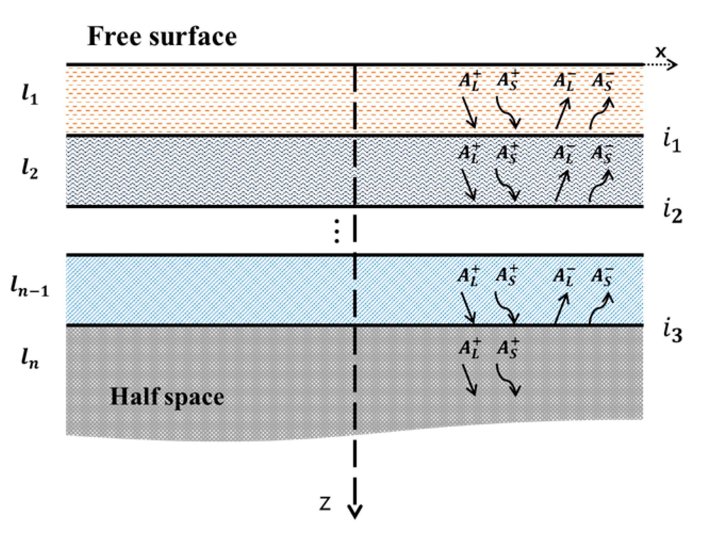
2.1. Dispersion Characteristics of Multilayer Thin Film
2.2. Modeling the Adhesion Interlayer
3. Experimental Setup and Method
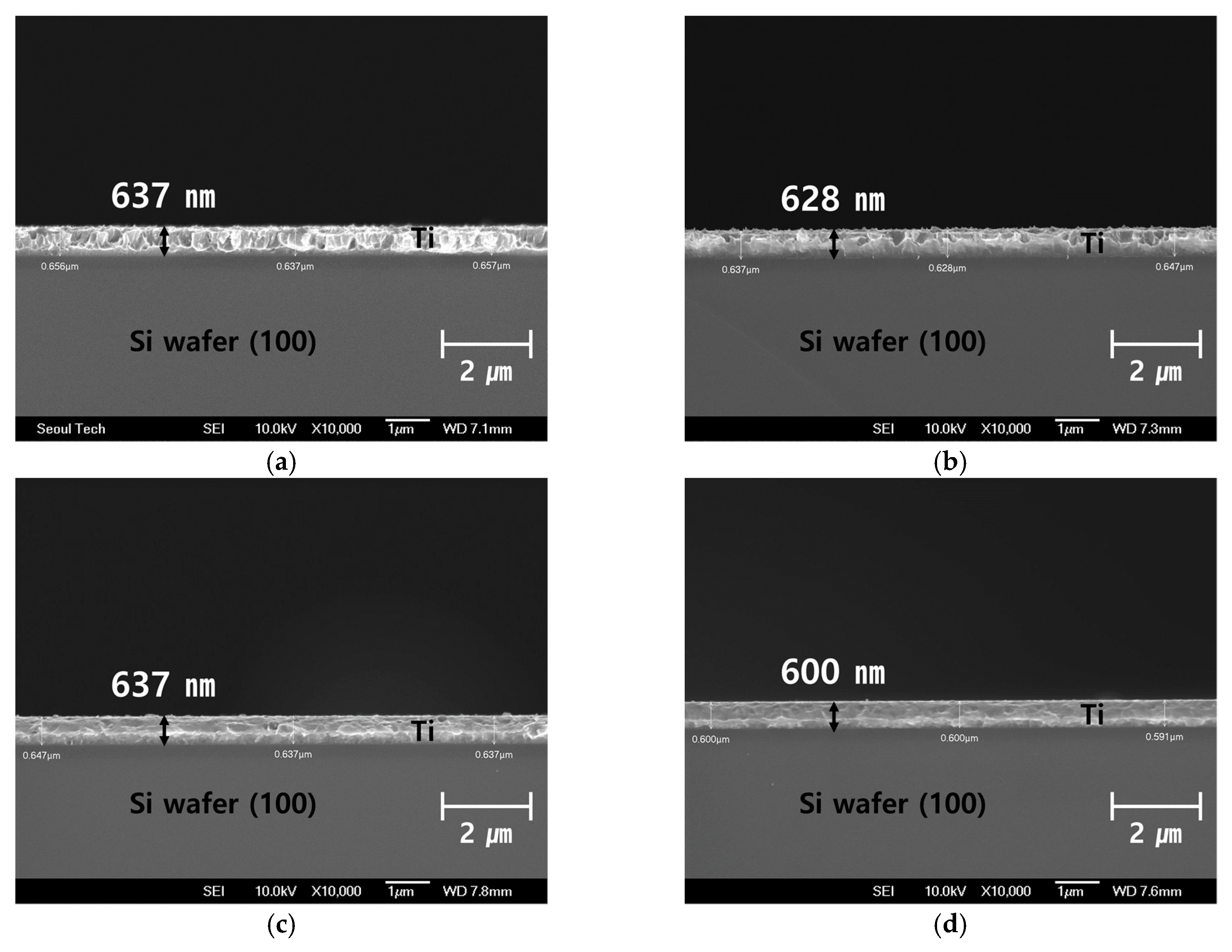
3.1. Preparation of Specimen
3.2. Surface Acoustic Wave Velocity Measurement Using a Scanning Acoustic Microscope
3.3. Evaluation of Stiffness Coefficient Using Dispersion Characteristics
3.4. Adhesion Force Evaluation by Nano-Scratch Test
4. Conclusions
Author Contributions
Funding
Institutional Review Board Statement
Informed Consent Statement
Data Availability Statement
Conflicts of Interest
References
- Mittal, K.L. Adhesion measurement of thin films. Electrocompon. Sci. Technol. 1976, 3, 21–42. [Google Scholar] [CrossRef]
- Park, T.S.; Kwak, D.R.; Park, I.K.; Miyasaka, C. Evaluation of adhesive strength for nano-structured thin film by scanning acoustic microscope. J. Korean Soc. Nondestruct. Test. 2012, 32, 393–400. [Google Scholar] [CrossRef]
- Tomastik, J.; Ctvrtlik, R.; Drab, M.; Manak, J. On the importance of combined scratch/acoustic emission test evaluation: SiC and SiCN thin films case study. Coatings 2018, 8, 196. [Google Scholar] [CrossRef]
- Du, J.; Tittmann, B.R.; Ju, H.S. Evaluation of film adhesion to substrates by means of surface acoustic wave dispersion. Thin Solid Films 2010, 518, 5786–5795. [Google Scholar] [CrossRef]
- Steinmann, P.A.; Tardy, Y.; Hintermann, H.E. Adhesion testing by the scratch test method: The influence of intrinsic and extrinsic parameters on the critical load. Thin Solid Films 1987, 154, 333–349. [Google Scholar] [CrossRef]
- Othman, M.F.; Bushroa, A.R.; Abdullah, W.N.R. Evaluation techniques and improvements of adhesion strength for TiN coating in tool applications: A review. J. Adhes. Sci. Technol. 2015, 29, 569–591. [Google Scholar] [CrossRef]
- Rahmati, B.; Sarhan, A.A.; Zalnezhad, E.; Kamiab, Z.; Dabbagh, A.; Choudhury, D.; Abas, W.A.B.W. Development of tantalum oxide (Ta-O) thin film coating on biomedical Ti-6Al-4V alloy to enhance mechanical properties and biocompatibility. Ceram. Int. 2016, 42, 466–480. [Google Scholar] [CrossRef]
- Grossmann, M.; Schubert, M.; He, C.; Brick, D.; Scheer, E.; Hettich, M.; Gusev, V.; Dekorsy, T. Characterization of thin-film adhesion and phonon lifetimes in Al/Si membranes by picosecond ultra-sonics. New J. Phys. 2017, 19, 053019. [Google Scholar] [CrossRef]
- Robin, M.; Jenot, F.; Ouaftouh, M.; Duquennoy, M. Influence of the laser source position on the generation of Rayleigh modes in a layer-substrate structure with varying degrees of adhesion. Ultrasonics 2020, 102, 106051. [Google Scholar] [CrossRef]
- Jenot, F.; Fourez, S.; Ouaftouh, M.; Duquennoy, M. Nondestructive testing of thin films using surface acoustic waves and laser ultrasonics. AIP Conf. Proc. 2018, 1949, 230031. [Google Scholar]
- Rajanna, P.M.; Luchkin, S.; Larionov, K.V.; Grebenko, A.; Popov, Z.I.; Sorokin, P.B.; Danilson, M.; Bereznev, S.; Lund, P.D.; Nasibulin, A.G. Adhesion of single-walled carbon nanotube thin films with different materials. J. Phys. Chem. Lett. 2020, 11, 504–509. [Google Scholar] [CrossRef]
- Aijaz, A.; Ferreira, F.; Oliveira, J.; Kubart, T. Mechanical properties of hydrogen free diamond-like carbon thin films deposited by high power impulse magnetron sputtering with Ne. Coatings 2018, 8, 385. [Google Scholar] [CrossRef]
- Park, T.S.; Choi, Y.M.; Cho, B.S.; Park, I.K. Analysis of Dispersion Characteristics of Rayleigh Waves in Nanostructured Thin Films. Korean Soc. Nondestruct. Test 2018, 38, 98–106. [Google Scholar] [CrossRef]
- Lowe, M.J. Matrix techniques for modeling ultrasonic waves in multilayered media. IEEE Trans. Ultrason. Ferroelectr. Freq. Control 1995, 42, 525–542. [Google Scholar] [CrossRef]
- Haskell, N.A. The dispersion of surface waves on multilayered media. Bull. Seismol. Soc. Am. 1953, 43, 17–34. [Google Scholar] [CrossRef]
- Tian, R.; Nie, G.; Liu, J.; Pan, E.; Wang, Y. On Rayleigh waves in a piezoelectric semiconductor thin film over an elastic half-space. Int. J. Mech. Sci. 2021, 204, 106565. [Google Scholar] [CrossRef]
- Baik, J.M.; Thompson, R.B. Ultrasonic scattering from imperfect interfaces: A quasi-static model. J. Nondestruct. Eval. 1984, 4, 177–196. [Google Scholar] [CrossRef]
- Kumar, S.A.; Sudheer, G. Influence of the oxide layer on the quality of bonding in adhesively bonded metallic structures by ultrasonic guided waves. Int. J. Adhes. Adhes. 2021, 111, 102981. [Google Scholar] [CrossRef]
- Le Crom, B.; Castaings, M. Shear horizontal guided wave modes to infer the shear stiffness of adhesive bond layers. J. Acoust. Soc. Am. 2010, 127, 2220–2230. [Google Scholar] [CrossRef]
- Tanabe, H.; Miyoshi, Y.; Takamatsu, T.; Sugiura, H. Effects of bias voltage and discharge current on mechanical properties of TiN film deposited by DC magnetron sputtering. J. Soc. Mater. Sci. Jpn. 2003, 52, 143–148. [Google Scholar] [CrossRef]
- Burnett, P.J.; Rickerby, D.S. The relationship between hardness and scratch adhesion. Thin Solid Films 1987, 154, 403–416. [Google Scholar] [CrossRef]


| Interfacial Condition | Boundary Stiffness | Longitudinal Velocity | Shear Velocity |
|---|---|---|---|
| Perfect bond | Boundary continuity | - | - |
| Complete debonding | = 0 | 0 | 0 |
| level 1 | = 61.44 | 14,120 | 7530 |
| level 2 | = = 15.36 | 7060 | 3770 |
| level 3 | = = 3.84 | 3530 | 1880 |
| level 4 | = 0.69 | 1760 | 940 |
| level 5 | = 0.24 | 880 | 470 |
| Specimen | DC Power Condition(W) | ||||
|---|---|---|---|---|---|
| 28.8 | 57.6 | 86.4 | 115.2 | 144 | |
| ) | 1.6065 | 1.1508 | 1.3125 | 1.0038 | 0.9429 |
| ) | 0.459 | 0.329 | 0.375 | 0.287 | 0.269 |
| Tip Type | |
|---|---|
| Initial load (mN) | 0.01 |
| Final load (mN) | 300 |
| Loading rate (mN/s) | 2.5 |
| /s) | 2 |
| ) | 350 |
| Specimen | DC Power Condition (W) | |||||
|---|---|---|---|---|---|---|
| 28.8 | 57.6 | 86.4 | 115.2 | 144 | ||
| 1.6065 | 1.1508 | 1.3125 | 1.0038 | 0.9429 | ||
| 0.459 | 0.329 | 0.375 | 0.287 | 0.269 | ||
| Critical load (mN) | 199.95 | 166.61 | 183.57 | 157.11 | 148.99 | |
Publisher’s Note: MDPI stays neutral with regard to jurisdictional claims in published maps and institutional affiliations. |
© 2022 by the authors. Licensee MDPI, Basel, Switzerland. This article is an open access article distributed under the terms and conditions of the Creative Commons Attribution (CC BY) license (https://creativecommons.org/licenses/by/4.0/).
Share and Cite
Choi, Y.M.; Kang, D.; Kim, J.N.; Park, I.K. Evaluation of Adhesion Properties of Thin Film Structure through Surface Acoustic Wave Dispersion Simulation. Materials 2022, 15, 5637. https://doi.org/10.3390/ma15165637
Choi YM, Kang D, Kim JN, Park IK. Evaluation of Adhesion Properties of Thin Film Structure through Surface Acoustic Wave Dispersion Simulation. Materials. 2022; 15(16):5637. https://doi.org/10.3390/ma15165637
Chicago/Turabian StyleChoi, Yu Min, Dongchan Kang, Jeong Nyeon Kim, and Ik Keun Park. 2022. "Evaluation of Adhesion Properties of Thin Film Structure through Surface Acoustic Wave Dispersion Simulation" Materials 15, no. 16: 5637. https://doi.org/10.3390/ma15165637
APA StyleChoi, Y. M., Kang, D., Kim, J. N., & Park, I. K. (2022). Evaluation of Adhesion Properties of Thin Film Structure through Surface Acoustic Wave Dispersion Simulation. Materials, 15(16), 5637. https://doi.org/10.3390/ma15165637