Abstract
The high efficiency of perovskite solar cells strongly depends on the quality of perovskite films and carrier extraction layers. Here, we present the results of an investigation of the photoelectric properties of solar cells based on perovskite films grown on compact and mesoporous titanium dioxide layers. Kinetics of charge carrier transport and their extraction in triple-cation perovskite solar cells were studied by using transient photovoltage and time-resolved photoluminescence decay measurements. X-ray diffraction analysis revealed that the crystallinity of the perovskite films grown on mesoporous titanium dioxide is better compared to the films grown on compact TiO2. Mesoporous structured perovskite solar cells are found to have higher power conversion efficiency mainly due to enlarged perovskite/mesoporous -TiO2 interfacial area and better crystallinity of their perovskite films.
1. Introduction
It has become increasingly urgent to look for renewable energy sources and improve the existing ones due to the ever-increasing energy demand accompanied by the exhaustion of organic fuels, global warming, and the current political situation. One of the most promising and environmentally friendly energy sources is electricity generated by solar cells. The organic–inorganic hybrid perovskite-based solar cells (PSC) show a promising future for photovoltaic technology [1]. During the last decade, the power conversion efficiency (PCE) of PSCs has grown from 3.8% to more than 25.7% [2], making them a very rapidly advancing technology and a popular topic in the field of solar cells. The high performance of PSCs can primarily be attributed to their excellent optoelectronic properties, such as (1) strong light absorption through the entire visible spectrum range, enabling the use of thin perovskite films [3,4]; (2) high carrier mobility [5,6]; (3) long carrier diffusion length [7,8]; (4) high defect tolerance [9]; and (5) long lifetime of the generated charge carriers [10,11]. To realize the good performance of a PSC, high-quality perovskite film containing a low density of defects must be employed in a single device [12]. The defects in a perovskite layer may affect both charge carrier transport and their extraction processes [13], and they can induce trap states, causing increased charge carrier recombination rate and, thereby, the reduced power conversion efficiency of a PSC [14]. To obtain perfectly operating perovskite devices, carrier transport and extraction layers are also important in addition to high-quality perovskite films [15,16]. There are several basic requirements for the transport layers: (1) good energy-level alignment with a perovskite for efficient charge transfer, (2) high mobility of charge carriers to guarantee their fast transport, (3) high transmittance to reduce the optical energy loss, (4) good stability, and (5) easy processing and low cost [16]. Two typical PSC structures are widely used: one is a planar heterojunction architecture [7,17], and another is a mesoporous structure [18,19]. Planar perovskite solar cells are advantageous because they have simple and scalable configurations [20]. However, the highest PCE is achieved with mesoscopic PSC, in which a mesoporous metal oxide layer plays an important role as the charge transport channel, scaffold for loading the light-absorbing materials, and electron–hole separator [21].
Titanium dioxide (TiO2) has been mostly used as an electron transport layer (ETL) in PSCs due to its wide bandgap, Eg = 3.2 eV, suitable for minimized parasitic absorption, an appropriate conduction band alignment with a perovskite for efficient electron injection, and good electron-transport capability [22]. The quality of ETL plays an important role in improving the performance of PSCs [23]. An ETL transports photoinduced electrons away from the perovskite, and at the same time, it serves as a blocking layer preventing direct contact between the holes and fluorine-doped tin oxide (FTO) [24,25]. Therefore, TiO2 layers should be uniform, pinhole-free, and should completely cover the surface of FTO [26]. The optimal thickness of crystalline TiO2 depends on the deposition technique and post-treatment of the layers. In the case of planar PSCs, the thickness of an ETL is in the range of 20–30 nm [26,27,28]. The deposition of a mesoporous (mp-TiO2) layer on crystalline titanium dioxide provides a reduced carrier transport length and increased interfacial contact area, thereby facilitating efficient charge carrier collection and yielding the highest reported PCE values [29]. It has been shown that the structural properties of the mp-TiO2 layer, such as particle size, thickness, and porosity, have a significant influence not only on the performance of PSCs but also on the layer’s photoelectric properties [13,26,30,31,32]. The transient photovoltage (TPV) measurements showed that the TPV decay strongly depends on the porosity of TiO2 film, and there is a significant correlation between the TPV decay characteristics and the performance of the perovskite solar cells [13]. It was established that the time-resolved photoluminescence (TRPL) decay also strongly depends on the size of TiO2 nanoparticles [30], the porosity of the TiO2 film, mesoscopic structure, and perovskite morphology formed therein [13]. TRPL spectroscopy is a powerful technique to study excited charge carrier recombination in perovskite layers that notably determine the PCE of PSCs [14].
In this paper, we report experimental results of the kinetics of the charge carrier transport and their extraction obtained by performing transient photovoltage and time-resolved photoluminescence decay measurements with the intention to elucidate the correlation between the electronic processes in perovskite layers and the performance of perovskite solar cells.
2. Fabrication of Perovskite Films and Their Characterization
In this study, two types of perovskite solar cells, with and without a porous TiO2 layer, were fabricated. Their schematic configurations are shown in Figure 1. The cells also differ in the formation and composition of the compact TiO2 layer: in one case, the compact TiO2 layers were formed by the conventional spray pyrolysis method; in another case, the compact TiO2 layers containing niobium oxide (Ti1–xNbxO2−mixed titanium niobium oxide) were deposited using the Atomic Layer Deposition (ALD) method. In both cases, the 25 × 25 mm2 glasses coated with a transparent fluorine-doped tin oxide (FTO) layer (TEC 10, Ossila, UK) were used as substrates. The composition of precursors, their concentrations and purity grades, the sequence of procedures and equipment, and the parameters of the layers (ETL, perovskite layer, and hole transport layer), all used for the fabrication of the perovskite cells, are detailed in our previous papers [33,34].
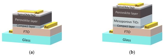
Figure 1.
Schematic configuration of the cells fabricated for the study: (a) without porous TiO2 layer, (b) with porous TiO2 layer. The compact TiO2 layers with and without Nb2O5 were formed using the ALD and spray pyrolysis methods, respectively.
Thin, compact Ti0.93Nb0.07O2 layers were deposited in a “Fiji F200” ALD reactor (Cambridge Nano Tech, Cambridge, MA, USA) using similar procedures as described in [35]. Precursors for titanium and niobium oxides were tetrakis dimethylamino titanium (TDMAT, 99.9%; STREM Chemicals Inc., Newburyport, MA, USA) and niobium ethoxide (Nb(OEt)5, 99.9%; STREM Chemicals Inc., Newburyport, MA, USA), and deionized water was used as an oxygen source. The mixed oxide was formed by depositing a single layer of niobium oxide for every 20 layers of deposited titanium oxide. The deposition consisted of 420 monolayers and resulted in an approximately 30 nm-thick coating.
We should note that porous TiO2, perovskite, and hole transport layers were formed over the ALD-mixed titanium niobium oxide layer using the same precursors and procedures as in the case of compact TiO2 layers formed by spray pyrolysis. Cs-containing Csx(MA0.17FA0.83)1–xPb(I0.83Br0.17)3 perovskite layers of the same composition with x = 0.1 were grown for both cell types. The 70 nm-thick Au contacts were deposited in the vacuum chamber of the thermal evaporation equipment “VAKSIS PVD Vapor-5S_Th” (Vaksis R&D and Engineering, Ankara, Turkey) on the top of the hole transport layer (Spiro-OMeTAD from Sigma-Aldrich, St. Louis, MO, USA, was used for its formation) and on the open side of FTO (see Figure 1).
The surface morphology and cross-section of the films were examined using a scanning electron microscope (SEM) (Helios NanoLab 650, FEI, Hillsboro, OR, USA).
X-ray diffraction (XRD) patterns were obtained using an X-ray diffractometer (XRD) (SmartLab, Rigaku, Tokyo, Japan) equipped with a 9 kW power rotating Cu anode X-ray source and theta/theta goniometer. The patterns were measured with Bragg–Brentano geometry in the 2Θ range of 10–65°.
The transient photovoltage of the solar cells was measured using the setup shown in Figure 2. A diode-pumped, frequency-doubled Nd:YAG-LBO laser NL202 (Ekspla Ltd., Vilnius, Lithuania) generated 7 ns-long pulses of 532 nm radiation. To prevent the sample from heating, a low pulse repetition rate of 5 Hz was used. A harmonic separator (dichroic beamsplitter; Eksma Ltd., Vilnius, Lithuania) was employed to reflect the rest of the infrared beam and transmit the 532 nm radiation. A part of the laser beam was directed to an optical signal reference detector (Standa Ltd., Vilnius, Lithuania) using a beam splitter plate. A variable attenuator (Eksma Ltd., Vilnius, Lithuania) consisting of a Brewster-type polarizer and quartz half wave-plate allowed changing the power of the incident laser beam. The average power of the laser radiation was measured by an optical power meter PM400 (Thorlabs Inc., Newton, NJ, USA). The maximum power density incident on the sample was about 0.5 mWcm−2. A laser beam was directed onto the sample S with a removable high-reflectance mirror (M). The transient photovoltage and the laser pulse were recorded using a digital storage oscilloscope DSO6102A (Agilent Technologies Inc., Santa Clara, CA, USA), and the laser pulse shape was registered by the high-speed detector 11HSP-FS1 (Standa Ltd., Vilnius, Lithuania).
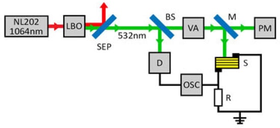
Figure 2.
The scheme of the experimental setup of transient photovoltage measurement. NL202 is the diode-pumped Nd:YAG laser; LBO is the nonlinear crystal for the second harmonic generation; SEP is the Nd:YAG laser harmonic separator; BS is the beam splitter plate; VA is the variable attenuator for 532 nm laser beam; M is the removable high-reflectance mirror; S is the sample solar cell; R is the load resistor; PM is the optical power meter; D is the optical signal reference detector; OSC is the digital storage oscilloscope.
The light from a continuous-wave (CW) Ar-ion laser or pulsed 532 nm microchip laser (Standa Ltd., Vilnius, Lithuania) was used for excitation in a standard photoluminescence (PL) measurement setup with a 1 m monochromator and thermoelectrically cooled photomultiplier tube working in the photon counting regime. More details of this technique are described in our previous paper [36]. The power of the lasers was varied with a linear variable metallic neutral density filter. The samples were held in a vacuumed optical cryostat during all CWPL and time-resolved photoluminescence (TRPL) measurements at room temperature.
The photovoltaic characteristics of the perovskite solar cells were measured using Keithley 2602A (Keithley Instruments Inc., Cleveland, OH, USA) equipment. The 100 mW/cm2 irradiance was produced by an AM 1.5 spectral lamp (Newport model 67005, Newport Corp., Irvine, CA, USA) placed at an appropriate distance.
3. Results and Discussion
Figure 3 presents the XRD patterns of the Ti0.93Nb0.07O2 film before (as-deposited) and after annealing in an H2 atmosphere at 400 °C for 50 min. The ramping-up rate was 5 °C/min, and the ramping-down rate was 3 °C per minute. It can be seen that the XRD pattern of the as-deposited film presents only FTO peaks. The XRD peaks of TiO2 (anatase) emerged on the XRD pattern of the Ti0.93Nb0.07O2 film annealed in a H2 atmosphere. The electrical resistivity of the Ti0.93Nb0.07O2 film decreased from 2 × 10² to 3.5 × 10⁻³ Ω cm during the annealing.
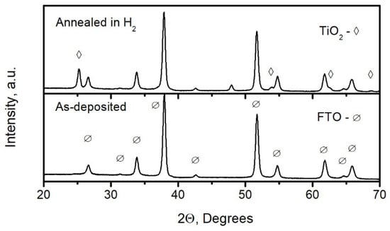
Figure 3.
XRD patterns of the Ti0.93Nb0.07O2 film before (as-deposited) and after annealing in a H2 atmosphere.
The top-view SEM images of the triple cation perovskite films grown on titanium dioxide using different methods are shown in Figure 4. The first perovskite (Film A) was grown on a compact titanium dioxide (c-TiO2) layer formed by the conventional spray pyrolysis method (FTO/c-TiO2/perovskite). The second perovskite film (Film B) was grown on the mesoporous TiO2 layer (FTO/c-TiO2/mp-TiO2/perovskite). The third perovskite film (Film C) was grown on the compact TiO2 layer deposited using the ALD method (FTO/ALD-TiO2/perovskite). The fourth perovskite film (Film D) was grown on the mesoporous TiO2 layer (FTO/ALD-TiO2/mp-TiO2/perovskite). It can be seen that the morphology of the perovskite films and grain sizes are similar and the surfaces are flat and smooth, in agreement with other reports elsewhere [23,32].
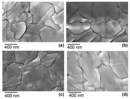
Figure 4.
Surface SEM images of perovskite films grown on different types of titanium dioxide layers: (a) Film A on the c-TiO2 layer, (b) Film B on the mp-TiO2 layer/c-TiO2, (c) Film C on the compact ALD-TiO2 layer, and (d) Film D on the mp-TiO2 layer/ALD-TiO2.
The cross-sectional SEM images of the same perovskite films are shown in Figure 5. It is seen that the morphology and grain distribution in the films grown on the compact TiO2 are similar (Figure 5a,c). The thickness of Films A and C was (880 ± 30) nm and (1200 ± 50) nm, respectively. However, the interface between Film A and c-TiO2 formed by spray pyrolysis (Figure 5a) contained some small cavities. The perovskite material grown on mesoporous TiO2 has penetrated between the nanocrystals of the mp-TiO2 layer (Figure 5b,d). The thickness of Films B and D was (880 ± 50) nm and (720 ± 50) nm, respectively. Though the surface images of the perovskite films (Figure 4) show grains with dimensions greater than 1000 nm, the cross-section images show that the films were composed of stacked grains but not of ones spanning over the whole thickness of the layer (Figure 5b,d).
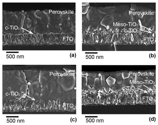
Figure 5.
Cross-sectional SEM images of perovskite films on different TiO2 layers: (a) Film A on the compact TiO2 layer, (b) Film B on the mp-TiO2 layer/c-TiO2, (c), Film C on the compact ALD-TiO2 layer, and (d) Film D on the mp-TiO2 layer/ALD-TiO2.
The XRD patterns of the perovskite films grown on different TiO2 layers are depicted in Figure 6. Most of the XRD peaks corresponded to 2Θ values of the cubic FA5/6Ma1/6PbBr0.5I2.5 phase (ICDD PDF card #01-085-6374). The rest of the peaks were attributable to FTO. Visually, the XRD patterns of the films were very similar. However, in the case of Film C, the perovskite XRD peak 100 was of higher intensity than peak 110, in contrast to the other patterns. This could mean that the crystallites of the Film C have a prevailing orientation in the [100] direction while the rest of the films have another prevailing orientation, namely, [110].
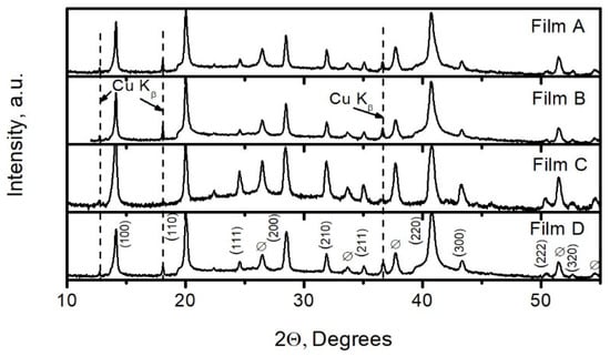
Figure 6.
XRD patterns of perovskite films on different titanium dioxide layers: Film A is on the compact TiO2 layer, Film B is on the mp-TiO2 layer/c, Film C is on the compact ALD-TiO2 layer, and Film D is on the ALD-TiO2/mp-TiO2 layer.
The XRD peaks of the perovskite films formed on TiO2 by spray pyrolysis seem to be sharper. This means that the crystallinity of the perovskite films grown on mesoporous titanium dioxide is better compared to the films grown on compact TiO2. The values of full width at half-maximum (FWHM) of the perovskite peaks 100, 110, and 220 are presented in Table 1. The size of a crystallite, D, and the value of micro-deformation, Δd/d (d is the interplanar spacing), both calculated using the Hall method, are also presented in the table. The FWHM values of Films A and B were smaller in comparison to those formed using the ALD method (Films C and D). Respectively, the size of crystallites was larger, and microdeformation was smaller in Films A and B, thus pointing to lower dislocation density in these films.

Table 1.
The FWHM values of perovskite XRD peaks 100, 110, and 220, crystallite size D, and the value of microdeformation Δd/d in different perovskite films.
Figure 7 shows CW photoluminescence spectra measured from both sides of the planar and mesoporous structured solar cells. For most of the samples, the peak position of the top side (spiro-OMeTAD side) spectrum is within the ±3 nm range centered at 762 nm. This finding agrees well with the other results of triple cation perovskites containing 10% of Cs [34,37]. However, the 10 nm blue shift is detected in the case of the Film C sample. Nevertheless, the peak position of the bottom side (glass side) is less scattered among the samples (Figure 7b), but it is slightly redshifted compared to the spiro-OMeTAD side case. Analyzing the “same side” PL results, one can observe that the peak position of the samples containing the mp-TiO2 layer has lower energy values than those of the samples with the c-TiO2 layer; but, again, except for the sample with Film C from the spiro-OMeTAD side. A study of the integrated PL intensity IPL dependence on laser power density P in the 1 mW/cm2 to 65 mW/cm2 range revealed that the Film C sample has the weakest dependence: its slope coefficient k () equals 0.95 when measured from the spiro-OMeTAD side. The coefficient k values are presented in Table 2. As a rule, the slope is below 1 for the free-to-bound and donor–acceptor transitions, and stays between 1 and 2 for the free-exciton or bound-exciton transitions [38]. The magnitude of k depends on the power density P and on material properties such as radiative and competitive nonradiative recombination probabilities [39] or the contribution of deep defects [40]. All these anomalies of Film C could be related to the smaller size of its crystallites. Therefore, a blue shift is observed in the CWPL spectrum from the spiro-OMeTAD side, and it changes the recombination probabilities, leading to a lower k value. Additionally, the decrease in the k value could result from donor–acceptor or free-bound transitions, including the contribution of the deep defects.
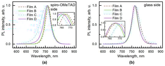
Figure 7.
CWPL spectra of PSC measured from (a) Spiro-OMeTAD side and (b) Glass side. Dashed and solid lines indicate planar and mesoporous structured cells, respectively. The insets show the corresponding enlarged part of peak position.
Table 2.
Results of PL spectra analysis. k is the slope of log IPL versus log P curve; Ai and τi are the amplitude and the decay time constant of the ith term in Equation (1); τdec is average decay time calculated using Equation (2).
Time-resolved photoluminescence decays measured both from spiro-OMeTAD and glass sides under a pulsed laser fluence of 0.1 μJ/cm2 are displayed in Figure 8. It shows the results of the longest average decay times obtained at different positions of all 20 samples (five samples from each series were tested). The transients were fitted using triple exponential approximation [33,41,42],
where fitting parameters Ai and τi are the amplitude and the decay time constant of the ith term. The fitting results according to Equation (1) are displayed in Figure 8 as a dotted line. The fitting parameters and the calculated average decay time,
are presented in Table 2. One can conclude that longer decay times are typical of perovskites on mesoporous TiO2 (samples Film B and D lead against Film A and C, respectively) and of layers formed using the conventional spray pyrolysis method (samples Film A and B lead against Film C and D, respectively). Meanwhile, Film C demonstrates the shortest decay times that can be influenced by the carrier surface recombination, which correlates with the results of structure analysis. The triple exponential fitting model is not good enough in some cases. Thus, we should additionally consider the processes of trapping and de-trapping [14].
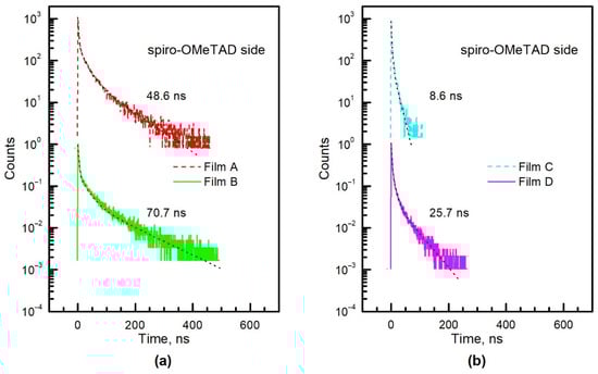
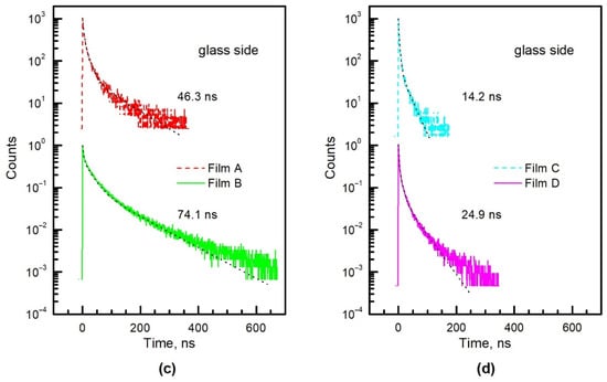
Figure 8.
PL decay transients of PSC measured from the spiro-OMeTAD side (a,b) and from the glass side (c,d). Black dotted lines indicate triple exponent approximation fitting, and the numbers (in ns) are the averaged decay time constants.
Photovoltage decay transients of the solar cells fabricated on different perovskite films are depicted in Figure 9. The photovoltage reaches its maximum value with a delay of approximately 100 to 200 ns after laser excitation. The dependence of photovoltage on time can be described by the following equation [13]:
where τt is the time constant of electron transport inside the perovskite layer, τrec is the electron recombination time, and V0 is the initial photovoltage. Fitting results calculated according to Equation (3) are depicted in Figure 9 as a dotted line. The redistribution of excited charge carriers inside the perovskite layer is determined mainly by their diffusion since the electric field is weak here. Therefore, τt is approximately equal to L2/D, where L is the layer thickness and D is the bipolar diffusion coefficient. The estimated D values are 0.12, 0.07, 0.25, and 0.07 cm2/s for perovskite samples Film A, B, C, and D, respectively. These values of bipolar diffusion coefficient are typical of spin-coated perovskite layers [5,7,43,44,45]. It should be noted that the diffusion coefficient is higher in planar than in mesoporous structured perovskite solar cells, as was observed earlier in [44], whereas the lifetime of generated charge carriers is longer in mesoporous structured perovskite solar cells due to the better crystallinity of mesoporous structured perovskite films.
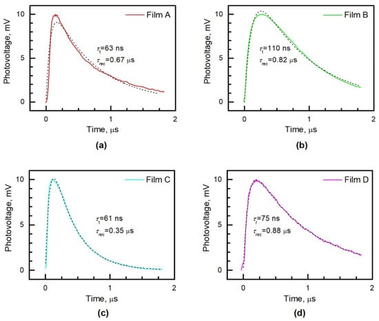
Figure 9.
Photovoltage decay transients of the solar cells fabricated on the base of different perovskite films: (a) Film A, (b) Film B, (c) Film C, (d) Film D. Black dotted lines indicate fitting according to Equation (3), and τt and τrec are the electron transport and recombination time constants, respectively.
The current versus forward bias voltage characteristics of the solar cells fabricated on different perovskite films are presented in Figure 10. It can be seen that the mesoporous structured PSCs show better performance than the planar ones. The values of photovoltaic quantities of the best PSCs are presented in Table 3, and statistics of the power-conversion efficiency of 60 perovskite solar cells fabricated on different perovskite films are depicted in Figure 11. The high PCE of mesoporous structured perovskite solar cells is mainly determined by a high value of the short circuit current resulting from an enlarged perovskite/mp-TiO2 interfacial area compared to the planar PSC case.
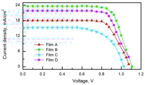
Figure 10.
Current–voltage characteristics of the solar cells fabricated on different perovskite films under 100 mW/cm2 spectral lamp irradiance.
Table 3.
Photovoltaic parameters of the solar cells on the base of different perovskite films. Voc is the open-circuit voltage; Jsc is the short circuit current; FF is the fill factor; PCE is the power-conversion efficiency.
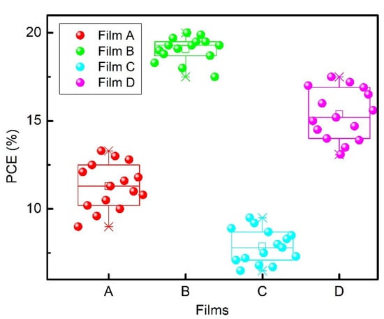
Figure 11.
Statistical distribution of the power-conversion efficiency of perovskite solar cells based on different perovskite films.
It is worth noting that the high crystallinity of mesoporous structured perovskite also has a positive effect on the performance of PSCs because uniform perovskite films with high surface coverage and minimum defects are beneficial for the transportation of both electrons and holes [46]. Additionally, time-resolved photoluminescence decay and transient photovoltage measurements showed that the lifetime of generated charge carriers in mesoporous structured perovskite solar cells is longer than that in planar PSCs, and as a consequence, the performance of the mesoporous structured PSCs is better. Negligible hysteresis of the current–voltage characteristics of the perovskite Cs0.1(MA0.17FA0.83)0.9Pb(I0.83Br0.17)3 solar cells is also a noteworthy fact, which was observed earlier in other works [33,37,47]. The planar PSCs fabricated on the base of Films A and C show the lowest PCE values, and this finding can be related to the shorter lifetime of charge carriers in these films resulting from their lower crystallinity (see Figure 8 and Figure 9). On the other hand, the mesoporous structured perovskite solar cells fabricated on the base of Film B demonstrate the best PCE due to the high crystallinity of the perovskite film, giving a reason for the long lifetime of the generated charge carriers. In addition, the crystallites of Film B are the largest (see Table 1). This also greatly contributes to the improved performance of the mesoporous structured perovskite solar cells [47]. Thus, we see a good correlation between electronic processes in perovskite layers and the performance of perovskite solar cells.
4. Conclusions
An experimental study of the photoelectric properties of planar and mesoporous structured perovskite solar cells was conducted. It was established that the crystallinity of perovskite films grown on mesoporous titanium dioxide is better than that of films grown on a compact TiO2. Transient photovoltage and time-resolved photoluminescence decay measurements show that the lifetime of charge carriers is also longer in mesoporous structured PSCs. The presented experimental data reveal the relationship between photovoltage decay characteristics and PSC performance, as both of them are affected by the mesoscopic structure of the layered structure. It was found that the mesoporous structured perovskite solar cells have a higher PCE than the planar ones, mainly due to an enlarged perovskite/mp-TiO2 interfacial area and longer lifetime of generated charge carriers. These results provide a basis for improved further material growth and device fabrication to achieve better performance of perovskite solar cells.
Author Contributions
Conceptualization and methodology, S.A. and K.L.; sample fabrication, A.G., K.P., L.S. and A.Š.; formal analysis, A.S. (Algirdas Selskis), A.S. (Algirdas Sužiedėlis) and J.G.; experimental investigation, E.Š., K.P., A.Č., R.J. and A.L.; writing, reviewing and editing, S.A., J.G. and K.L.; visualization, A.S. (Algirdas Selskis) and K.P.; project administration and supervision, S.A. All authors have read and agreed to the published version of the manuscript.
Funding
This research was funded by the Research Council of Lithuania, grant number 01.2.2-LMT-K-718-01-0050.
Institutional Review Board Statement
Not applicable.
Informed Consent Statement
Not applicable.
Data Availability Statement
No new data were created or analyzed in this study. Data sharing is not applicable to this article.
Acknowledgments
We are sincerely thankful to Skaidra Bumelienė for her good will in the preparation of the article manuscript.
Conflicts of Interest
The authors declare no conflict of interest.
References
- Mozaffari, N.; Walter, D.; White, T.P.; Bui, A.D.; Tabi, G.D.; Weber, K.; Catchpole, K.R. Unraveling the role of energy band alignment and mobile ions on interfacial recombination in perovskite solar cells. Sol. RRL 2022, 6, 2101087. [Google Scholar] [CrossRef]
- Kim, M.; Jeong, J.; Lu, H.; Lee, T.K.; Eickemeyer, F.T.; Liu, Y.; Choi, I.W.; Choi, S.J.; Jo, Y.; Kim, H.B.; et al. Conformal Quantum Dot-SnO2 Layers as Electron Transporters for Efficient Perovskite Solar Cells. Science 2022, 375, 302–306. Available online: https://www.science.org/doi/10.1126/science.abh1885 (accessed on 24 April 2022). [CrossRef] [PubMed]
- De Wolf, S.; Holovsky, J.; Moon, S.-J.; Löper, P.; Niesen, B.; Ledinsky, M.; Haug, F.-J.; Yum, J.-H.; Ballif, C. Organometallic halide perovskites: Sharp optical absorption edge and its relation to photovoltaic performance. J. Phys. Chem. Lett. 2014, 5, 1035–1039. [Google Scholar] [CrossRef] [PubMed]
- Quan, L.N.; Rand, B.P.; Friend, R.H.; Mhaisalkar, S.G.; Lee, T.W.; Sargent, E.H. Perovskites for next-generation optical sources. Chem. Rev. 2019, 119, 7444–7478. [Google Scholar] [CrossRef]
- Wehrenfennig, C.; Eperon, G.E.; Johnston, M.B.; Snaith, H.J.; Herz, L.M. High carrier mobilities and lifetimes in organolead trihalide perovskites. Adv. Mater. 2014, 26, 1584–11589. [Google Scholar] [CrossRef]
- Karakus, M.; Jensen, S.A.; D’Angelo, F.; Turchinovich, D.; Bonn, M.; Cánovas, E. Phonon-electron scattering limits free charge mobility in methylammonium lead iodide perovskites. J. Phys. Chem. Lett. 2015, 6, 4991–4996. [Google Scholar] [CrossRef]
- Stranks, S.D.; Eperon, G.E.; Grancini, G.; Menelaou, C.; Alcocer, M.J.P.; Leijtens, T.; Herz, L.M.; Petrozza, A.; Snaith, H.J. Electron-hole diffusion lengths exceeding 1 micrometer in an Organometal trihalide perovskite absorber. Science 2013, 342, 341–344. [Google Scholar] [CrossRef]
- Dong, Q.; Fang, Y.; Shao, Y.; Mulligan, P.; Qiu, J.; Cao, L.; Huang, J. Electron-hole diffusion lengths > 175 µm in solution-grown CH3NH3PbI3 single crystals. Sci. Express 2015, 347, 967–969. [Google Scholar] [CrossRef]
- Kothandaraman, R.K.; Jiang, Y.; Feurer, T.; Tiwari, A.N.; Fu, F. Near-infrared-transparent perovskite solar cells and peroskite-based tandem photovoltaics. Small Methods 2020, 4, 2000395. [Google Scholar] [CrossRef]
- Staub, F.; Hempel, H.; Hebig, J.C.; Mock, J.; Paetzold, U.W.; Rau, U.; Unold, T.; Kirchartz, T. Beyond bulk lifetimes: Insights into lead halide perovskite films from time-resolved photoluminescence. Phys. Rev. Appl. 2016, 6, 044017. [Google Scholar] [CrossRef]
- Solanki, A.; Yadav, P.; Turren-Cruz, S.H.; Lim, S.S.; Saliba, M.; Sum, T.C. Cation influence on carrier dynamics in perovskite solar cells. Nano Energy 2019, 58, 604–611. [Google Scholar] [CrossRef]
- Xie, Y.M.; Xue, Q.; Yip, H.L. Metal-halide perovskite krystallzation kinetics: A review of experimental and theoretical studies. Adv. Energy Mater. 2021, 11, 2100784. [Google Scholar] [CrossRef]
- Hydayat, R.; Nurunnizar, A.A.; Fariz, A.; Herman; Rosa, E.S.; Shobih; Oizumi, T.; Fujii, A.; Ozaki, M. Revealing the charge carrier kinetics in perovskite solar cells affected by mesoscopic stuctures and defect states from simple transient photovoltage measurements. Sci. Rep. 2020, 10, 19197. [Google Scholar] [CrossRef] [PubMed]
- Pean, E.V.; Dimitrov, S.; de Castro, C.S.; Davies, M.L. Interpreting time-resolved photoluminescence of perovskite materials. Phys. Chem. Chem. Phys. 2020, 22, 28345. [Google Scholar] [CrossRef]
- Lian, J.; Lu, B.; Niu, F.; Zeng, P.; Zhan, X. Electron-transport materials in perovskite solar cells. Small Methods 2018, 2, 1800082. [Google Scholar] [CrossRef]
- Zhao, Y.; Ye, Q.; Chu, Z.; Gao, F.; Zhang, X.; You, J. Recent progress in high-efficiency planar-structure perovskite solar cells. Energy Environ. Mater. 2019, 2, 93–106. [Google Scholar] [CrossRef]
- Liu, M.; Johnston, M.B.; Snaith, H.J. Efficient planar heterojunction perovskite solar cells by vapour deposition. Nature 2013, 501, 395–398. [Google Scholar] [CrossRef]
- Kim, H.S.; Lee, C.R.; Im, J.H.; Lee, K.B.; Moehl, T.; Marchioro, A.; Moon, S.J.; Humphry-Baker, R.; Yum, J.H.; Moser, J.E.; et al. Lead iodide perovskite sensitized all-solid-state submicron thin film mesoscopic solar cell with efficiency exceeding 9%. Sci. Rep. 2012, 2, 591. [Google Scholar] [CrossRef]
- Lee, M.M.; Teuscher, J.; Miyasaka, T.; Murakami, T.N.; Snaith, H.J. Efficient hybrid solar cells based on meso-superstructured organometal halide perovskites. Science 2012, 338, 643–647. [Google Scholar] [CrossRef]
- Li, Y.; Cooper, J.K.; Buonsanti, R.; Giannini, C.; Liu, Y.; Toma, F.M.; Sharp, I.D. Fabrication of planar heterojunction perovskite solar cells by controlled low-pressure vapor annealing. J. Phys. Chem. Lett. 2015, 6, 493–499. [Google Scholar] [CrossRef]
- Lee, D.G.; Kim, M.; Kim, B.J.; Kim, D.H.; Lee, S.M.; Choi, M.; Lee, S.; Jung, H.S. Effect of TiO2 particle size and layer thickness on mesoscopic perovskite solar cells. Appl. Surf. Sci. 2019, 477, 131–136. [Google Scholar] [CrossRef]
- Kim, J.Y.; Lee, J.W.; Jung, H.S.; Shin, H.; Park, N.G. High-efficiency perovskite solar cells. Chem. Rev. 2020, 120, 7867–7918. [Google Scholar] [CrossRef] [PubMed]
- Wang, J.; Zou, X.; Zhu, J.; Cheng, J.; Chen, D.; Bai, X.; Yao, Y.; Chang, C.; Yu, X.; Liu, B.; et al. Effect of optimization of TiO2 electron transport layer on performance of perovskite solar cells with rough FTO substrates. Materials 2020, 13, 2272. [Google Scholar] [CrossRef] [PubMed]
- Marchioro, A.; Teuscher, J.; Friedrich, D.; Kunst, M.; Krol, R.; Moehl, T.; Grätzel, M.; Moser, J.-E. Unravelling the mechanism of photoinduced charge transfer processes in lead iodide perovskite solar cells. Nat. Photonics 2014, 8, 250–255. [Google Scholar] [CrossRef]
- Starowicz, Z.; Gawlińska, K.; Walter, J.; Socha, R.P.; Kulesza-Matlak, G.; Lipiński, M. Extended investigation of sol aging effect on TiO2 electron transporting layer and performances of perovskite solar cells. Mater. Res. Bull. 2018, 99, 136–143. [Google Scholar] [CrossRef]
- Sławek, A.; Starowicz, Z.; Lipiński, M. The influence of the thickness compact TiO2 electron transporting layer on the performances of planar CH3NH3PbI3 perovskite solar cells. Materials 2021, 14, 3295. [Google Scholar] [CrossRef]
- Xiao, M.; Huang, F.; Huang, W.; Dkhissi, Y.; Zhu, Y.; Etheridge, J.; Gray-Weale, A.; Bach, U.; Cheng, Y.-B.; Spiccia, L. A fast deposition-crystallization procedure for highly efficient lead iodide perovskite thin-film solar cells. Angew. Chem. Int. Ed. Engl. 2014, 53, 9898–9903. [Google Scholar] [CrossRef]
- Saliba, M.; Correa-Baena, J.-P.; Wolff, C.M.; Stolterfoht, M.; Phung, N.; Albrecht, S.; Neher, D.; Abate, A. How to make over 20% efficient perovskite solar cells in regular (n–i–p) and inverted (p–i–n) architectures. Chem. Mater. 2018, 30, 4193–4201. [Google Scholar] [CrossRef]
- Grätzel, M. The light and shade of perovskite solar cells. Nat. Mater. 2014, 13, 838–842. Available online: www.nature.com/articles/nmat4065 (accessed on 25 April 2022). [CrossRef]
- Yang, Y.; Ri, K.; Mei, A.; Liu, L.; Hu, M.; Liu, T.; Li, X.; Han, H. The size effect of TiO2 nanoparticles on a printable mesoscopic perovskite solar cell. J. Mater. Chem. 2015, 3, 9103–9107. [Google Scholar] [CrossRef]
- Hu, H.; Dong, B.; Hu, H.; Chen, F.; Kong, M.; Zhang, Q.; Luo, T.; Zhao, L.; Guo, Z.; Li, J.; et al. Atomic layer deposition of TiO2 for a high-efficiency hole-blocking layer in hole-conductor-free perovskite solar cells processed in amber air. Appl. Mater. Interfaces 2016, 8, 17999–18007. [Google Scholar] [CrossRef] [PubMed]
- Sun, X.; Xu, J.; Xiao, L.; Chen, J.; Zhang, B.; Yao, J.; Dai, S. Influence of the porosity of the TiO2 film on the performance of the perovskite solar cells. Int. J. Photoenergy 2017, 2017, 4935265. [Google Scholar] [CrossRef]
- Ašmontas, S.; Čerškus, A.; Gradauskas, J.; Grigucevičienė, A.; Leinartas, K.; Lučun, A.; Petrauskas, K.; Selskis, A.; Sužiedelis, A.; Širmulis, E.; et al. Cesium-containing triple cation perovskite solar cells. Coatings 2021, 11, 279. [Google Scholar] [CrossRef]
- Ašmontas, S.; Čerškus, A.; Gradauskas, J.; Grigucevičienė, A.; Juškėnas, R.; Leinartas, K.; Lučun, A.; Petrauskas, K.; Selskis, A.; Sužiedelis, A.; et al. Impact of cesium concentration on optoelectronic properties of metal halide perovskites. Materials 2022, 15, 1936. [Google Scholar] [CrossRef]
- Ašmontas, S.; Anbinderis, M.; Gradauskas, J.; Juškėnas, R.; Leinartas, K.; Lučun, A.; Selskis, A.; Staišiūnas, L.; Stanionytė, S.; Sužiedėlis, A.; et al. Low resistance TiO2/p-Si heterojunction for tandem solar cell. Materials 2020, 13, 2857. [Google Scholar] [CrossRef]
- Kundrotas, J.; Čerškus, A.; Valušis, G.; Linfield, E.H.; Johannessen, E.; Johannessen, A. Dynamics of free carriers-neutral impurity related optical transitions in Be and Si δ-doped GaAs/AlAs multiple quantum wells: Fractional-dimensional space approach. Lith. J. Phys. 2014, 54, 233–243. [Google Scholar] [CrossRef][Green Version]
- Saliba, M.; Matsui, T.; Seo, J.Y.; Domaski, K.; Correa-Baena, J.-P.; Nazeeruddin, M.K.; Zakeeruddin, S.M.; Tress, W.; Abate, A.; Hagfeldt, A.; et al. Cesium-containing triple cation perovskite solar cells: Improved stability, reproducibility and high efficiency. Energy Environ. Sci. 2016, 9, 1989–1997. [Google Scholar] [CrossRef]
- Schmidt, T.; Lischka, K.; Zulehner, W. Excitation-power dependence of the near-band-edge photoluminescence of semiconductors. Phys. Rev. B 1992, 45, 8989–8994. [Google Scholar] [CrossRef]
- Shibata, H.; Sakai, M.; Yamada, A.; Matsubara, K.; Sakurai, K.; Tampo, H.; Ishizuka, S.; Kim, K.-K.; Niki, S. Excitation-power dependence of free exciton photoluminescence of semiconductors. Jpn. J. Appl. Phys. 2005, 44, 6113–6114. [Google Scholar] [CrossRef]
- Spindler, C.; Galvani, T.; Wirtz, L.; Rey, G.; Siebentritt, S. Excitation-intensity dependence of shallow and deep-level photoluminescence transitions in semiconductors. J. Appl. Phys. 2019, 126, 175703–175709. [Google Scholar] [CrossRef]
- Dursun, I.; Zheng, Y.; Guo, T.; de Bastiani, M.; Turedi, B.; Sinatra, L.; Haque, M.A.; Sun, B.; Zhumekenov, A.A.; Saidaminov, M.I.; et al. Efficient photon recycling and radiation trapping in cesium lead halide perovskite waveguides. ACS Energy Lett. 2018, 3, 1492–1498. [Google Scholar] [CrossRef]
- Ca, N.X.; Hien, N.T.; Luyen, N.T.; Lien, V.T.K.; Thanh, L.D.; Do, P.V.; Bau, N.Q.; Pham, T.T. Photoluminescence properties of CdTe/CdTeSe/CdSe core/alloyed/shell type-II quantum dots. J. Alloys Compd. 2019, 787, 823–830. [Google Scholar] [CrossRef]
- Leijtens, T.; Stranks, S.D.; Eperon, G.E.; Lindblad, R.; Johansson, E.M.J.; McPherson, I.J.; Rensmo, H.; Ball, J.M.; Lee, M.M.; Snaith, H.J. Electronic properties of meso-superstructured and planar organometal halide perovskite films:charge trapping, photodoping, and carrier mobility. ACS Nano 2014, 8, 7147–7155. [Google Scholar] [CrossRef] [PubMed]
- Hutter, E.M.; Eperon, G.E.; Stranks, S.D.; Savenije, T.J. Charge carrier in planar and meso-structured organic-inorganic perovskites: Mobilities, lifetimes, and concentrations of trap states. J. Phys. Chem. Lett. 2015, 6, 3082–3090. [Google Scholar] [CrossRef] [PubMed]
- Ščajev, P.; Qin, C.; Aleksiejūnas, R.; Baronas, P.; Miasojedovas, S.; Fujihara, T.; Matsushima, T.; Adachi, C.; Juršėnas, S. Diffusion enhancement in highly excited MAPbI3 perovskite layers with additives. J. Phys. Chem. Lett. 2018, 9, 3167–3172. [Google Scholar] [CrossRef]
- Li, Y.; Ji, L.; Liu, R.; Zhang, C.; Mak, C.H.; Zou, X.; Shen, H.H.; Leu, S.Y.; Hsu, H.Y. A revew on morphology engineering for highly efficient and stable hybrid perovskite solar cells. J. Mater. Chem. A 2018, 6, 12842–12875. [Google Scholar] [CrossRef]
- Singh, T.; Miyasaka, T. Stabilizing the efficiency beyond 20% with a mixed cation perovskite solar cell in ambient air under controlled humidity. Adv. Energy Mat. 2018, 8, 1700677. [Google Scholar] [CrossRef]
Publisher’s Note: MDPI stays neutral with regard to jurisdictional claims in published maps and institutional affiliations. |
© 2022 by the authors. Licensee MDPI, Basel, Switzerland. This article is an open access article distributed under the terms and conditions of the Creative Commons Attribution (CC BY) license (https://creativecommons.org/licenses/by/4.0/).