Article

Towards Interband Cascade lasers on InP Substrate

Department of Experimental Physics, Faculty of Fundamental Problems of Technology, Wrocław University of Science and Technology, Wybrzeże Wyspiańskiego 27, 50-370 Wroclaw, Poland
*
Author to whom correspondence should be addressed.
Materials 2022, 15(1), 60; https://doi.org/10.3390/ma15010060
Submission received: 17 November 2021 / Revised: 14 December 2021 / Accepted: 17 December 2021 / Published: 22 December 2021
(This article belongs to the Special Issue Semiconductor Quantum Wells and Superlattices)

Abstract

:
In this study, we propose designs of an interband cascade laser (ICL) active region able to emit in the application-relevant mid infrared (MIR) spectral range and to be grown on an InP substrate. This is a long-sought solution as it promises a combination of ICL advantages with mature and cost-effective epitaxial technology of fabricating materials and devices with high structural and optical quality, when compared to standard approaches of growing ICLs on GaSb or InAs substrates. Therefore, we theoretically investigate a family of type II, “W”-shaped quantum wells made of InGaAs/InAs/GaAsSb with different barriers, for a range of compositions assuring the strain levels acceptable from the growth point of view. The calculated band structure within the 8-band k·p approximation showed that the inclusion of a thin InAs layer into such a type II system brings a useful additional tuning knob to tailor the electronic confined states, optical transitions’ energy and their intensity. Eventually, it allows achieving the emission wavelengths from below 3 to at least 4.6 μm, while still keeping reasonably high gain when compared to the state-of-the-art ICLs. We demonstrate a good tunability of both the emission wavelength and the optical transitions’ oscillator strength, which are competitive with other approaches in the MIR. This is an original solution which has not been demonstrated so far experimentally. Such InP-based interband cascade lasers are of crucial application importance, particularly for the optical gas sensing.

1. Introduction

An important class of coherent radiation sources in the mid-wave infrared have become the interband cascade lasers (ICLs) employing type II, indirect in the real space optical transitions [1,2]. The concept of ICL is beneficial with respect to some of the device performances, i.e., it combines a voltage-efficient cascading scheme, borrowed from the quantum cascade lasers, and a long upper-level recombination lifetime as in a conventional diode laser. The ICLs are usually based on a broken gap material system of InAs/GaInSb [1,2,3,4], which fulfills the electronic structure and technological requirements, and simultaneously allows to reach a broad range of mid infrared (MIR) [5]. The ICLs have already been demonstrated to operate in continuous wave and single mode at room temperature, or even above, in the spectral range from below 3 to above 6 μm [6,7,8,9,10,11] and record low power consumption (<0.1 W at threshold at 300 K), ultralow threshold current densities as for MIR lasers [6,12] as well as high cw output powers [4]. These characteristics translate into numerous applications of ICLs, including in optical gas sensing [13,14], multi-gas analyzers [15], industrial process control [16,17], environmental pollution monitoring [18], medical diagnostics [19], infrared countermeasures [20], gas leakage detection [21], free space optical communication [22] with demonstrations of the efficient optical wireless link for military applications [23], combustion diagnostics [24], IR scene projection [25], and detection of explosives [26].
Current ICLs are grown by molecular beam epitaxy on GaSb or InAs substrates. In spite of all their abovementioned achievements, there remain applications-driven further demands to improve the active material and the device characteristics or to reduce the fabrication costs. These would potentially be obtainable when ICLs could be grown in mature and cheaper technologies based on GaAs or InP. As for the case of GaAs-substrate some preliminary demonstrations exist—an ICL in a pulsed mode and low temperatures (up to 270 K) has been reported [27], such are still missing for the case of InP-based technology. The latter, which is also cost-effective, offers additional advantages like simplified epitaxial structure, because the InP can also serve as an optical cladding layer, improved heat dissipation material or allows considering the option of using a high-power near-IR sources to optically pump an epitaxial-side-down-mounted device through a transparent substrate [28]. Overall, such a novel ICL would be a breakthrough solution because InP-substrate-based laser devices of various architectures have only been demonstrated significantly below 3 μm [29,30,31,32], with slightly longer wavelengths achieved in photoluminescence measurements (PL) [29,32,33,34] (see also Table 1 where the current status of the InP-based quantum well (QW) structures predicted for emission above 2 μm is summarized), including an example of spontaneous emission from a type II GaInAs/GaAsSb QW at 3.9 μm [32].
The latter example indicates the potential of this material’s’ combination among other proposed solutions for the MIR range. There have been reported a couple of simulated designs of type I or type II lasers’ active regions involving various materials matching the InP technology to extend the emission wavelengths [28,33,35,36,37], but they have never been translated into operational devices. The reasons they have not been successful are manifold: the proposed materials are of insufficient structural or optical quality (e.g., the dilute nitrides or dilute bismides), the electronic confinement of one type of carriers is too weak, or the strain is too high, or a combination of several of these. Therefore, searching for new solutions is still necessary—within the considered systems, the one employing InGaAs/GaAsSb seems to stand out.
In our studies, we have mainly been inspired by the work from [33], which had shown that InP-based type-II InGaAs/GaAsSb heterostructures are promising for emission or detection for λ around 2 μm, plus that they offer relatively low net strain, i.e., more favorable material growth that allows to avoid the potential strain relaxation. The main objective of our current work is to propose such a type II active area QW structure that would allow emission in the application-relevant range, which could further be directly used to fabricate operational ICLs of that kind in low-cost, mature InP-substrate-based technology. We propose several designs of the active region made of InGaAs, GaAsSb and AlAsSb layers and model the respective electronic and optical properties. We mainly concentrate on extension of the emission wavelength to the range of about 3–5 µm, because it is especially relevant for applications in the optical laser-based gas sensing, as many of the environmentally or medically important gasses have their strongest absorption lines there. It is also one of the windows of the free space optical communication. We originally propose to include a thin InAs layer, which becomes an additional tuning knob to tailor the electronic structure and to reach easier the longer wavelengths of above 4 μm. We demonstrate for the first time that using the approach with such an especially modified type II InGaAs/GaAsSb active region compatible with an InP substrate should allow the fabricating of the interband cascade lasers emitting in the target MIR region, with expected performances competitive to the state of the art devices on GaSb substrate, meanwhile being significantly cheaper in production.

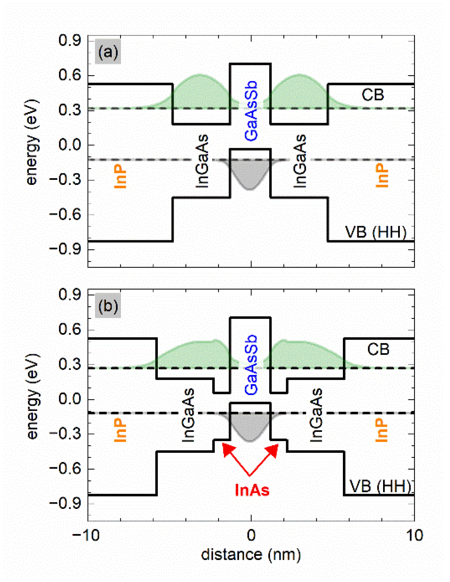
2. Materials and Methods
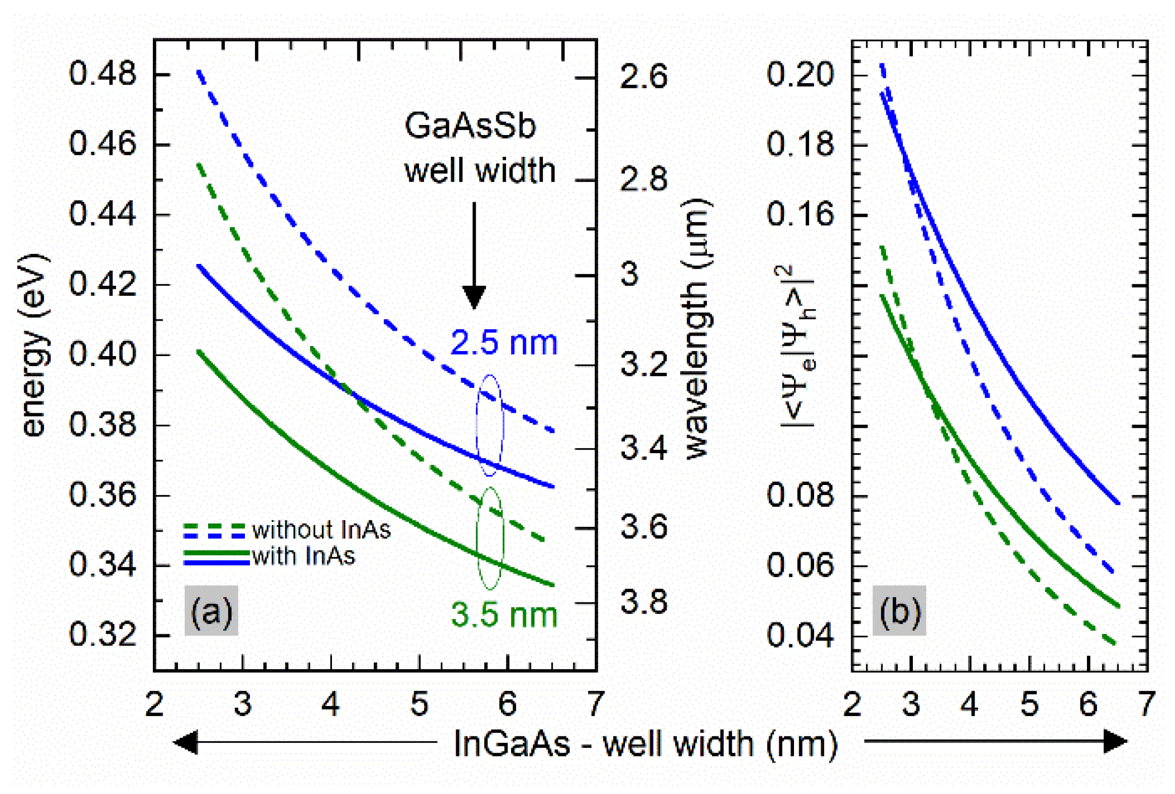
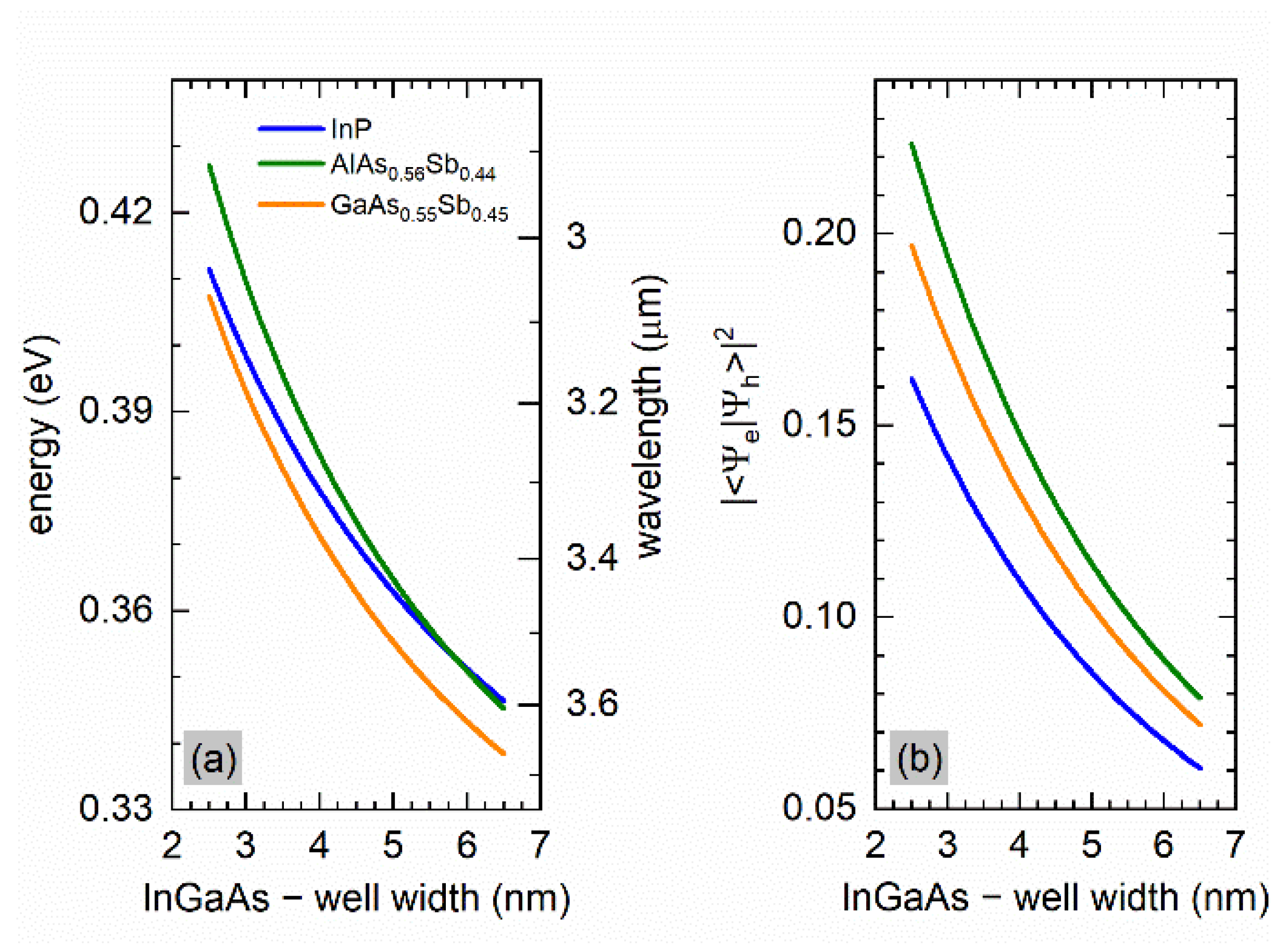
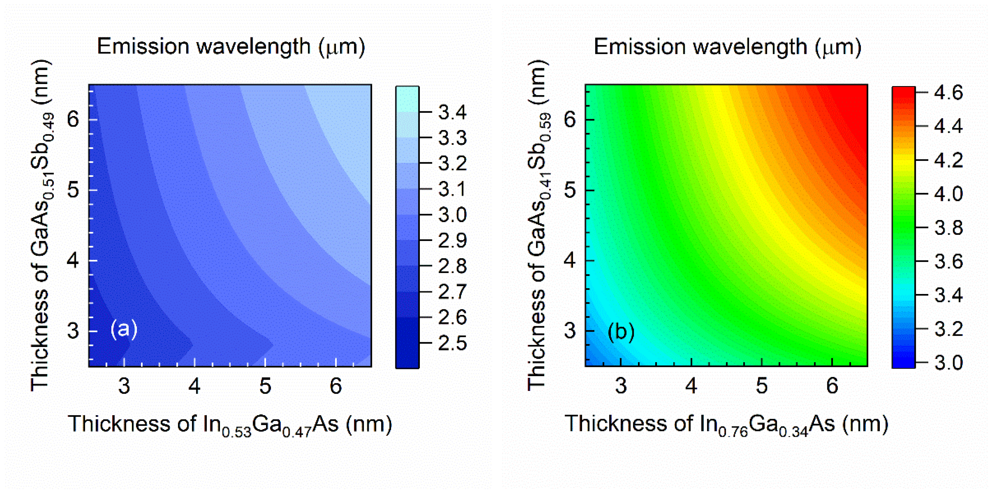
We began the considerations with calculating the band structure and wave functions near the center of the Brillouin Zone. The eight-band k·p model within the envelope function approximation was used to calculate the electron and hole energy levels (subbands) in an active region of an ICL on InP substrate. The total Hamiltonian for the strained QW, which describes the energy spectrum for both conduction and valence subbands, is given by [38]
H = H 8 × 8 + H S + V ( z ) ,
where H 8 × 8 is the 8 × 8 k·p Hamiltonian, H S is the corresponding strain Hamiltonian and V ( z ) describes the conduction and valence band offsets. In this case, for active region QW of an ICL structure, a net strain was obtained from the relations
ε = i L i ε i i L i
where L i and ε i are the thicknesses of layers forming the given part of the active region and the non-zero components of the strain tensor in the layer, respectively. The carrier wave functions and the subband energies are determined by numerically solving the Schrödinger equation employing the finite difference method (FDM). The FDM is suitable for this kind of calculation because it is fast and facilitates using an arbitrary mesh [39]. To calculate the electronic structure and wave functions we used the standard mathematical subroutines available in the LAPACK libraries [40]. To investigate the optical transitions, we mainly examined the matrix elements, which are primarily determined by the spatial overlap integral of the electron and hole wave functions. More details on the calculations’ methodology can be found in Refs. [38,41]. All the material parameters were taken from Refs. [42,43] for 300 K. The total gain was obtained by using the subband-to-subband optical transitions and which is described in Refs. [41,44]. We assume that the half linewidth of the Lorentzian function is equal to 5 meV, based on the transport data for n- and p-type InAs/Ga1−xInxSb superlattices of type II [45]. We present the results for TE polarization only.

3. Results

Figure 1a,b show the conduction and heavy-hole band edge profiles after including the strain, the fundamental electron e1 and heavy hole hh1 energy levels and the squared moduli of the corresponding wave functions (expressing the distribution of the probability densities) for two cases of the so called W-design structures (i.e., when using two QWs in the conduction band, such offer enhanced optical transition oscillator strengths while still keeping the type II lineup [5]). The first one is a strained type II QW, for which we chose the following compositions and thicknesses: In0.7Ga0.3As(3.5 nm)/GaAs0.45Sb0.55(2.5 nm)/In0.7Ga0.3As(3.5 nm) on InP substrate, Figure 1a (InP barriers). The calculated value of ε∗ is −0.96% in this case. The corresponding emission wavelength is about 2.82 µm at 300 K. As expected, the maxima of the squared wave function moduli can be found in the InGaAs and GaAsSb layers for electrons and holes, respectively.
In the second QW structure (Figure 1b), we propose to insert a thin InAs layer between the InGaAs and GaAsSb layers. Due to significant lattice mismatch between InAs and the InP substrate, and hence high strain, the used InAs layer thickness must be kept small, as it induces additional strain (here it is 1.0 nm). Comparing the structures presented in Figure 1a,b, we find that the calculated net strain changes from −0.96% to −1.35%, respectively. However, the advantage of the added InAs insertion is a significant red shift of the emission wavelength from 2.8 μm to 3.1 μm, which is targeted. This effect comes from changing the confinement for electrons via modifying the structure shown in Figure 1b. In particular, it can be observed that the addition of the InAs layer shifts the electron ground state down in energy and moves the maximum of the squared waves function moduli into the InAs layer. This in turn decreases the fundamental, type II optical transition energy and increases its intensity—both are beneficial in our case.
Figure 2a,b present the calculated dependence of the active transition energy and the squared overlap integral of the electron and hole wave functions on InGaAs layer thickness in this kind of W-design QWs, for the cases as presented in from Figure 1, i.e., without and with the InAs layer, respectively, for two different thicknesses of the quaternary GaAsSb layer. First, we find that the entire MIR range demanded by the applications can be covered spectrally by emission from such QWs. Second, it is seen that spatially indirect type-II recombination allows for even longer emission wavelengths when the additional InAs layer is included (Figure 2a), with even enlarged transition oscillator strength in the longer wavelengths range (Figure 2b). However, as mentioned above, the additional InAs layer causes higher average strain. But to minimize this effect, GaAsSb material with increased antimony content can be taken into account.
In Figure 3—similar to Figure 2—the calculated transition energy (wavelength) and overlap integrals are presented, but now it is for various external barrier materials (those directly surrounding the active regions in ICL structure). We consider just InP, but also two other alloys that are lattice-matched to InP, i.e., AlAs0.56Sb0.44 and GaAs0.55Sb0.45. It can be seen that with increasing width of the InGaAs quantum well, changing the barrier material from InP to AlAs0.56Sb0.44 does not bring the expected increase in emission wavelength. However, promising results are obtained when the surrounding of the active region is made of GaAs0.55Sb0.45. The effect of the type II structure modifications on the fundamental optical transitions oscillator strength, expressed by the squared overlap integral, is shown in Figure 3b. Particularly important is the fact that the transition intensity increases significantly for the latter barrier case. For comparison, in the case of structures grown on GaSb substrates, the transition intensity values (in sense of squared overlaps) are about 0.2 in a structure of AlSb/InAs(3.0 nm)/GaInSb(3.5 nm)/InAs(3.0 nm)/AlSb [38], about 0.3 for AlSb/InAs(3.0 nm)/GaAsSb(3.0 nm)/InAs(3.0 nm)/AlSb and about 0.2 for AlSb/InAs(3.0 nm)/GaAsSb(7.0 nm)/InAs(3.0 nm)/AlSb [46], and approx. 0.25 for the type-II W-design lattice-matched to GaSb [47]. This also holds true for the cases corresponding to longer wavelength emission, which shows directly the main advantage of using the materials proposed here to be deposited on the InP substrate.
Figure 4 presents the calculated In content dependence of the e1–hh1 transition energy in the type-II W-design GaAs0.55Sb0.45/InxGa1−xAs/InAs(1.0 nm)/GaAs0.45Sb0.55(3.5 nm)/InAs(1.0 nm)/InxGa1−xAs/GaAs0.55Sb0.45 QW for two different InxGa1−xAs widths. First, Figure 4a shows that the change of the composition in the confinement layer affects the transition energy significantly because of shifting the electron energy levels (the hole ones are almost unaffected), and hence allows for easy tunability in the target range of the MIR. This is due to a combined effect of both; the band gap change of the material but also the strain—changing the In content in InxGa1−xAs in the considered range means increasing the in-plane strain from 0.6% to 1.4%.
The effect of the type II structure modifications on the fundamental optical transitions oscillator strength is shown in Figure 4b. There can be mainly observed that the transition intensity decreases slightly when the In mole fraction increases from 40% to 80% in InxGa1−xAs (by a factor of 2–3). It can also be seen that when the InxGa1−xAs well width increases from 3.0 nm to 4.5 nm, the fundamental optical transitions oscillator strength increases, which can compensate for the intensity loss due to changes of the indium content. This shows the overall compositions and thicknesses range for possible tunability of this type of active region used in an ICL.
Then, we study the GaAs0.58Sb0.42/X/InAs(1.0 nm)/Y/InAs(1.0 nm)/X/GaAs0.58Sb0.4 system in a broader range of parameters in the type II W-structure on InP substrate (for X = In0.53Ga0.47As or In0.76Ga0.24As and Y = GaAs0.49Sb0.51 or GaAs0.41Sb0.59). Figure 5 illustrates a contour plot of the calculated emission wavelength dependence of the QW width in the conduction band (i.e., X-type material) versus valence band QW width (i.e., Y-type material). In the case when the material confining electrons is lattice matched to the substrate the emission wavelength reaches 3.5 µm, at most. A significantly different situation takes place when the confinement layer for electrons is made of a material that is compressively strained (net strain in the range from −0.98% to −1.23%)—then the emission wavelength can exceed 4 µm.
Figure 5b also shows that the emission wavelength is further red shifted when an additional InAs layer is inserted into the QW structure. In order to maximize the shift, we slightly modified the materials within the active region—for a QW made of GaAs0.58Sb0.42/In0.76Ga0.24As/InAs/GaAs0.41Sb0.59/InAs/In0.76Ga0.24As/GaAs0.58Sb0.42 the obtained emission wavelength is in the range from about 3.0 μm to 4.6 µm.
Eventually, for two selected cases, we have calculated the corresponding optical gain spectra (see Figure 6), i.e., for W-shaped QWs of GaAs0.58Sb0.42/In0.76Ga0.24As/GaAs0.41Sb0.59/In0.76Ga0.24As/GaAs0.58Sb0.42 without the InAs insertion (blue dashed line) and with the additional InAs layer (red solid line)—GaAs0.58Sb0.42/In0.76Ga0.24As/InAs/GaAs0.41Sb0.59/InAs/In0.76Ga0.24As/GaAs0.58Sb0.42 QW—the chosen layer thicknesses are given in the caption of Figure 6. The optical gain spectra have been calculated for an exemplary, but realistic injected carriers’ density of 3 × 1018 cm−3 at 300 K. The obtained maximum values of the gain equal about 40 cm—1, which is similar to those typically obtained for the type II active regions on GaSb or InAs substrates [28,45]. It is also clearly seen, in agreement with the discussion above, that adding the thin InAs layer increases the gain slightly and shifts it to longer wavelengths (by almost 0.4 μm in this particular case).

4. Conclusions

We have studied the influence of material configuration (compositions and layers’ thicknesses) on the electronic structure and the material gain of a type-II W-design QWs as the active region of an interband cascade laser, and considered their possible epitaxial deposition on InP substrates. The proposed original solution is based on a combination of InGaAs/GaAsSb materials, forming a broken gap layout, with an included additional InAs layer in the active part. We have chosen a set of parameters, including changes of the QW barrier material, which allow to combine the application-relevant spectral range with reasonably large transition oscillator strengths, and low enough net strain to assure the coherent growth without the strain relaxation. We have concentrated on the emission wavelengths of about 3–5 μm as it is the target range for many optical laser-based gas sensing applications and it is also one of the windows of the free space optical communication. These cause demands on new laser solutions with improved characteristics and lower fabrication costs. In that context, we have demonstrated for the first time that using the approach with particularly modified type II InGaAs/InAs/GaAsSb active region to be grown on an InP substrate should allow fabricating the interband cascade lasers with performances, which can be expected to be comparable to the state of the art devices on GaSb substrate, while also significantly cheaper and obtained in mature semiconductor technology. These translate into high structural and optical quality of the grown materials if only the strain is kept on an acceptable level, which we show is also possible. All these can be employed to fabricate MIR emitting InP-based ICLs, which have not been demonstrated so far. Such devices can directly be realized in practice in MBE or even MOCVD, as the growth of the materials under consideration is rather well-mastered, and hence it should be possible to also combine with the necessary injector layers and claddings. Therefore, we hope that our work will stimulate the experimental efforts, especially in the material development and device fabrication to grow such structures in order to verify our predictions, and will pave the way towards first real ICL devices compatible with InP substrates.

Author Contributions

Conceptualization, K.R. and G.S.; methodology, K.R.; software, K.R.; validation, K.R.; data analysis, K.R. and J.A.; investigation, J.A., K.R. and G.S.; resources, G.S.; writing—original draft preparation, K.R. and J.A.; writing—review and editing, G.S.; visualization, J.A.; funding acquisition, G.S. All authors have read and agreed to the published version of the manuscript.

Funding

The work has been supported by the Polish National Agency for Academic Exchange (Grant No. PPI/APM/2018/1/00031/U/001).

Institutional Review Board Statement

Not applicable.

Informed Consent Statement

Not applicable.

Data Availability Statement

The data that support the findings of this research are available from the corresponding author upon reasonable request.

Conflicts of Interest

The authors declare no conflict of interest.

References

  1. Yang, R.Q. Infrared laser based on intersubband transitions in quantum wells. Superlattices Microstruct. 1995, 17, 77. [Google Scholar] [CrossRef]
  2. Meyer, J.R.; Bewley, W.W.; Canedy, C.L.; Kim, C.S.; Kim, M.; Merritt, C.D.; Vurgaftman, I. The Interband Cascade Laser. Photonics 2020, 7, 75. [Google Scholar] [CrossRef]
  3. Bauer, A.; Rößner, K.; Lehnhardt, T.; Kamp, M.; Höfling, S.; Worschech, L.; Forchel, A. Mid-infrared semiconductor hetero-structure lasers for gas sensing applications. Semicond. Sci. Technol. 2011, 26, 014032. [Google Scholar] [CrossRef]
  4. Vurgaftman, I.; Weih, R.; Kamp, M.; Meyer, J.R.; Canedy, C.L.; Kim, C.S.; Kim, M.; Bewley, W.W.; Merritt, C.D.; Abell, J.; et al. Interband cascade lasers. J. Phys. D Appl. Phys. 2015, 48, 123001. [Google Scholar] [CrossRef]
  5. Motyka, M.; Ryczko, K.; Sęk, G.; Janiak, F.; Misiewicz, J.; Bauer, A.; Höfling, S.; Forchel, A. Type II quantum wells on GaSb substrate designed for laser-based gas sensing applications in a broad range of mid infrared. Opt. Mater. 2012, 34, 1107. [Google Scholar] [CrossRef]
  6. Dallner, M.; Hau, F.; Höfling, S.; Kamp, M. InAs-based interband-cascade-lasers emitting around 7 μm with threshold cur-rent densities below 1 kA/cm2 at room temperature. Appl. Phys. Lett. 2015, 106, 041108. [Google Scholar] [CrossRef] [Green Version]
  7. Kim, C.; Bewley, W.; Merritt, C.; Canedy, C.; Warren, M.; Vurgaftman, I.; Meyer, J.; Kim, M. Improved mid-infrared interband cascade light emitting devices. Opt. Eng. 2017, 57, 011002. [Google Scholar] [CrossRef]
  8. Scheuermann, J.; Weih, R.; Edlinger, M.; Nähle, L.; Fischer, M.; Koeth, J.; Kamp, M.; Höfling, S. Single-mode interband cascade lasers emitting below 2.8 μm. Appl. Phys. Lett. 2015, 106, 161103. [Google Scholar] [CrossRef] [Green Version]
  9. Weih, R.; Kamp, M.; Höfling, S. Interband cascade lasers with room temperature threshold current densities below 100 A/cm2. Appl. Phys. Lett. 2013, 102, 231123. [Google Scholar] [CrossRef] [Green Version]
  10. Bewley, W.; Canedy, C.; Kim, C.; Kim, M.; Merritt, C.; Abell, J.; Vurgaftman, I.; Meyer, J. Continuous-wave interband cascade lasers operating above room temperature at λ = 4.7 − 5.6 μm. Opt. Express 2012, 20, 3235. [Google Scholar] [CrossRef] [PubMed]
  11. Janiak, F.; Motyka, M.; Sęk, G.; Dyksik, M.; Ryczko, K.; Misiewicz, J.; Weih, R.; Höfling, S.; Kamp, M.; Patriarche, G. Effect of arsenic on the optical properties of GaSb-based type II quantum wells with quaternary GaInAsSb layers. J. Appl. Phys. 2013, 114, 223510. [Google Scholar] [CrossRef]
  12. Vurgaftman, I.; Bewley, W.W.; Canedy, C.L.; Kim, C.S.; Kim, M.; Merritt, C.D.; Abell, J.; Meyer, J.R. Interband cascade lasers with low threshold powers and high output powers. IEEE J. Sel. Top. Quantum Electron. 2013, 19, 1200210. [Google Scholar] [CrossRef]
  13. Dong, L.; Tittel, F.K.; Li, C.; Sanchez, N.P.; Wu, H.; Zheng, C.; Yu, Y.; Sampaolo, A.; Griffin, R.J. Compact TDLAS based sensor design using interband cascade lasers for mid-IR trace gas sensing. Optics Express 2016, 24, A528. [Google Scholar] [CrossRef]
  14. Kluczynski, P. Multi-laser in-situ analyzer for real time control of DESOX and DENOX processes in a waste incinerator plant. In Proceedings of the Annual ISA Analysis Division Symposium, Galveston, TX, USA, 6–8 May 2019; Volume 534, p. 12. [Google Scholar]
  15. Scheuermann, J.; Kluczynski, P.; Siembab, K.; Straszewski, M.; Kaczmarek, J.; Weih, R.; Fischer, M.; Koeth, J.; Schade, A.; Höfling, S. Interband Cascade Laser Arrays for Simultaneous and Selective Analysis of C1–C5 Hydrocarbons in Petrochemical Industry. Appl. Spectrosc. 2021, 75, 336–342. [Google Scholar] [CrossRef] [PubMed]
  16. Fang, B.; Yang, N.; Zhao, W.; Wang, C.; Zhang, W.; Song, W.; Venables, D.S.; Chen, W. Improved spherical mirror multi-pass-cell-based interband cascade laser spectrometer for detecting ambient formaldehyde at parts per trillion by volume levels. Appl. Opt. 2019, 58, 8743. [Google Scholar] [CrossRef] [PubMed]
  17. Rena, W.; Luo, L.; Tittel, F.K. Sensitive detection of formaldehyde using an interband cascade laser near 3.6 μm. Sens. Actuators 2015, B 221, 1062. [Google Scholar] [CrossRef]
  18. Wysocki, G.; Bakhirkin, Y.; So, S.; Tittel, F.K.; Hill, C.; Yang, R.Q.; Fraser, M.P. Dual interband cascade laser based trace-gas sensor for environmental monitoring. Appl. Opt. 2007, 46, 8202. [Google Scholar] [CrossRef] [Green Version]
  19. Ghorbani, R.; Schmidt, F.M. ICL-based TDLAS sensor for real-time breath gas analysis of carbon monoxide isotopes. Opt. Express 2017, 25, 12743–12752. [Google Scholar] [CrossRef]
  20. Höfling, S.; Weih, R.; Bauer, A.; Kamp, M.; Forchel, A. Room temperature continuous wave interband cascade lasers for gas sensing. Proc. SPIE 2012, 8432, 84320N1–84320N8. [Google Scholar] [CrossRef]
  21. Lundqvist, S.; Kluczyński, P.; Weih, R.; von Edlinger, M.; Nähle, L.; Fischer, M.; Bauer, A.; Höfling, S.; Koeth, J. Sensing of formaldehyde using a distributed feedback interband cascade laser emitting around 3493 nm. Appl. Opt. 2012, 51, 6009–6013. [Google Scholar] [CrossRef]
  22. Soibel, A.; Wright, M.W.; Farr, W.H.; Keo, S.A.; Hill, C.J.; Yang, R.Q.; Liu, H.C. Midinfrared Interband Cascade Laser for Free Space Optical Communication. IEEE Photonics Technol. Lett. 2010, 22, 121–123. [Google Scholar] [CrossRef]
  23. Mikołajczyk, J.; Weih, R.; Motyka, M. Optical Wireless Link Operated at the Wavelength of 4.0 µm with Commercially Available Interband Cascade Laser. Sensors 2021, 21, 4102. [Google Scholar] [CrossRef]
  24. Goldenstein, C.S.; Spearrin, R.M.; Jeries, J.B.; Hanson, R.K. Infrared laser-absorption sensing for combustion gases. Prog. Energy Combust. Sci. 2016, 60, 132–176. [Google Scholar] [CrossRef] [Green Version]
  25. Ejzak, G.A.; Dickason, J.; Marks, J.A.; Nabha, K.; McGee, R.T.; Waite, N.A.; Benedict, J.T.; Hernandez, M.A.; Provence, S.R.; Norton, D.T., Jr.; et al. 512 × 512, 100 Hz mid-wave infrared LED microdisplay system. J. Disp. Technol. 2016, 12, 1139–1144. [Google Scholar] [CrossRef]
  26. Fuchs, F.; Hugger, S.; Jarvis, J.; Yang, Q.K.; Ostendorf, R.; Schilling, C.; Bronner, W.; Driad, R.; Aidam, R.; Wagner, J. Imaging stando trace detection of explosives using IR-laser based backscattering. Proc. SPIE 2016, 9836, 983621. [Google Scholar] [CrossRef]
  27. Hill, C.J.; Yang, R.Q. Interband cascade lasers grown on GaAs substrates lasing at 4 microns. Appl. Phys. Lett. 2004, 85, 3014. [Google Scholar] [CrossRef]
  28. Vurgaftman, I.; Meyer, J.R.; Tansu, N.; Mawst, L.J. InP-based dilute-nitride mid-infrared type-II “W” quantum-well lasers. J. Appl. Phys. 2004, 96, 4653–4655. [Google Scholar] [CrossRef] [Green Version]
  29. Chang, C.H.; Li, Z.-L.; Pan, C.-H.; Lu, H.-T.; Lee, C.-P.; Lin, S.-D. Room-temperature mid-infrared “M”-type GaAsSb/InGaAs quantum well lasers on InP substrate. J. Appl. Phys. 2014, 115, 063104. [Google Scholar] [CrossRef] [Green Version]
  30. Sprengel, S.; Andrejew, A.; Federer, F.; Veerabathran, G.K.; Boehm, G.; Amann, M.-C. Continuous wave vertical cavity surface emitting lasers at 2.5 μm with InP-based type-II quantum wells. Appl. Phys. Lett. 2015, 106, 151102. [Google Scholar] [CrossRef]
  31. Gu, Y.; Zhanga, Y.G.; Ma, Y.J.; Zhou, L.; Chen, X.Y.; Xi, S.P.; Du, B. InP-based type-I quantum well lasers up to 2.9 μm at 230 K in pulsed mode on a metamorphic buffer. Appl. Phys. Lett. 2015, 106, 121102. [Google Scholar] [CrossRef]
  32. Sprengel, S.; Grasse, C.; Wiecha, P.; Andrejew, A.; Gruendl, T.; Boehm, G.; Meyer, R.; Amann, M.-C. InP-Based Type-II Quantum-Well Lasers and LEDs. IEEE J. Sel. Top. Quantum Electron. 2013, 19, 1900909. [Google Scholar] [CrossRef]
  33. Huang, J.Y.T.; Mawst, L.J.; Kuech, T.F.; Song, X.; Babcock, S.E.; Kim, C.S.; Vurgaftman, I.; Meyer, J.R.; Holmes, A.L., Jr. Design and characterization of strained InGaAs/GaAsSb type-II ’W’ quantum wells on InP substrates for mid-IR emission. J. Phys. D Appl. Phys. 2009, 42, 025108. [Google Scholar] [CrossRef]
  34. Sprengel, S.; Grasse, C.; Vizbaras, K.; Gruendl, T.; Amann, M.C. Up to 3 um light emission on InP substrate using GaInAs/GaAsSb type-II quantum wells. Appl. Phys. Lett. 2011, 99, 221109. [Google Scholar] [CrossRef]
  35. Gladysiewicz, M.; Kudrawiec, R.; Wartak, M.S. Electronic Band Structure and Material Gain of Dilute Nitride Quantum Wells Grown on InP Substrate. IEEE J. Quantum Electron. 2015, 51, 7100212. [Google Scholar] [CrossRef]
  36. Chen, B. Active Region Design and Gain Characteristics of InP-Based Dilute Bismide Type-II Quantum Wells for Mid-IR Lasers. IEEE Trans. Electron. Devices 2017, 64, 1606–1611. [Google Scholar] [CrossRef]
  37. Broderick, C.A.; Xiong, W.; Sweeney, S.J.; O’Reilly, E.P.; Rorison, J.M. Theory and design of InxGa1−xAs1−yBiy mid-infrared semiconductor lasers: Type-I quantum wells for emission beyond 3 μm on InP substrates. Semicond. Sci. Technol. 2018, 33, 094007. [Google Scholar] [CrossRef] [Green Version]
  38. Ryczko, K.; Sȩk, G.; Misiewicz, J. Eight-band k·p modeling of InAs/InGaAsSb type-II W-design quantum well structures for interband cascade lasers emitting in a broad range of mid infrared. J. Appl. Phys. 2013, 114, 223519. [Google Scholar] [CrossRef]
  39. Tan, I.H.; Snider, G.L.; Chang, L.D.; Hu, E.L. A self consistent solution of Schrödinger–Poisson equations using a nonuni-form mesh. J. Appl. Phys. 1990, 68, 4071. [Google Scholar] [CrossRef] [Green Version]
  40. LAPACK Users’ Guide (Third ed.). Available online: http://www.netlib.org/lapack/ (accessed on 10 September 2021).
  41. Ryczko, K.; Zielińska, A.; Sęk, G. Interband Cascade Active Region with Ultra-Broad Gain in the Mid-Infrared Range. Materials 2021, 14, 1112. [Google Scholar] [CrossRef] [PubMed]
  42. Jadczak, J.; Kubisa, M.; Ryczko, K.; Bryja, L.; Potemski, M. High magnetic field spin splitting of excitons in asymmetric GaAs quantum wells. Phys. Rev. B 2012, 86, 245401. [Google Scholar] [CrossRef]
  43. Vurgaftman, I.; Meyer, J.R.; Ram-Mohan, L.R. Band parameters for III–V compound semiconductors and their alloys. J. Appl. Phys. 2001, 89, 5815. [Google Scholar] [CrossRef] [Green Version]
  44. Chuang, S.L. Physics of Optoelectronic Devices, Wiley Series in Pure and Applied Optics; John Wiley & Sons: New York, NY, USA, 1995; Chapter 9. [Google Scholar]
  45. Hoffman, C.A.; Meyer, J.R.; Youngdale, E.R.; Bartoli, F.J.; Miles, R.H. Interface roughness scattering in semiconducting and semimetallic InAs-Ga1−xInxSb superlattices. Appl. Phys. Lett. 1993, 63, 2210. [Google Scholar] [CrossRef]
  46. Ryczko, K.; Sęk, G.; Misiewicz, J. Novel design of type-II quantum wells for mid-infrared emission with tensile-strained GaAsSb layer for confinement of holes. Appl. Phys. Express 2015, 8, 121201. [Google Scholar] [CrossRef]
  47. Ryczko, K.; Sęk, G. Towards unstrained interband cascade lasers. Appl. Phys. Express 2018, 11, 012703. [Google Scholar] [CrossRef]
Figure 1. Energy band diagram and the squared waves function moduli for an (a) InP/In0.7Ga0.3As(3.5 nm)/GaAs0.45Sb0.55(2.5 nm)/In0.7Ga0.3As(3.5 nm)/InP (b) InP/In0.7Ga0.3As(3.5 nm)/InAs/GaAs0.45Sb0.55(2.5 nm)/InAs/In0.7Ga0.3As(3.5 nm)/InP type II “W” QW along the growth direction.
Materials 15 00060 g001
Figure 2. (a) Calculated ground state transition emission energy and the related overlap integrals (b) for InP/In0.7Ga0.3As/GaAs0.45Sb0.55/In0.7Ga0.3As/InP type II “W” (short-dash lines) and for and InP/In0.7Ga0.3As/InAs/GaAs0.45Sb0.55/InAs/In0.7Ga0.3As/InP type II “W” (solid lines). The thickness of the InAs layer was 1.0 nm.
Materials 15 00060 g002
Figure 3. The fundamental transition energy (a) and the squared overlap integral (b) as a function of InGaAs well width in W-design (X)/In0.7Ga0.3As/InAs/GaAs0.45Sb0.55//InAs/In0.7Ga0.3As/(X), where (X) = InP (blue solid line), AlAs0.56Sb0.44 (green solid line), GaAs0.55Sb0.45 (orange solid line). The thicknesses of the InAs and GaAs0.45Sb0.55 layers were 1.0 nm and 3.0 nm.
Materials 15 00060 g003
Figure 4. Emission energy (a) and the squared overlap integral (b) for an GaAs0.55Sb0.45/InxGa1−xAs/InAs(1.0 nm)/GaAs0.45Sb0.55(3.5 nm)/InAs(1.0 nm)/InxGa1−xAs/GaAs0.55Sb0.45 type II “W” (solid line) of varying In mole fraction in InxGa1−xAs. The blue (orange) lines correspond to a 3.0(4.5)-nm-thick InxGa1−xAs layer.
Materials 15 00060 g004
Figure 5. Contour plots of emission wavelength at the zone center for (a) GaAs0.58Sb0.42/In0.53Ga0.47As/InAs(1.0 nm)/GaAs0.51Sb0.49/InAs(1.0 nm)/In0.53Ga0.47As/GaAs0.58Sb0.42 and (b) GaAs0.58Sb0.42/In0.76Ga0.24As/InAs(1.0 nm)/GaAs0.41Sb0.59/InAs(1.0 nm)/In0.76Ga0.24As/GaAs0.58Sb0.42 type II “W” type-II ‘W’ QW structures at 300 K, versus electron and hole well thicknesses.
Materials 15 00060 g005
Figure 6. Calculated optical gain spectra for GaAs0.58Sb0.42/In0.76Ga0.24As(4.0 nm)/GaAs0.41Sb0.59(3.0 nm)/In0.76Ga0.24As(4.0 nm)/GaAs0.58Sb0.42 and GaAs0.58Sb0.42/In0.76Ga0.24As(4.0 nm)/InAs(1.0 nm)/GaAs0.41Sb0.59(3.0 nm)/InAs(1.0 nm)/In0.76Ga0.24As(4.0 nm)/GaAs0.58Sb0.42 “W” design type-II ‘W’ QW structures.
Materials 15 00060 g006
Table 1. Summary of the current status on various approaches with QWs on InP substrate to reach the MIR emission.
Active RegionEmission Wavelength
(μm)
CommentsReferences
“M”-type GaAsSb/InGaAs quantum-well2.4–2.5Room temperature PL at 2.5 μm and optically pumped lasing at 2.41 μm[29]
W-shaped type II InGaAs/GaAsSb QWs∼2.5VCSEL device[30]
Type I InAs/InGaAs/InAlAs QWs∼2.9Low-temperature lasing in pulsed mode; growth on In0.8Al0.2As metamorphic buffer[31]
GaInAs/GaAsSb type-II quantum wells2.6–3.9Electrically pumped lasing in pulsed mode at 2.6 μm; spontaneous emission up to 3.9 μm[32]
InGaAs/GaAsSb type-II ‘W-design’ quantum wells> 2.0Room temperature PL at ∼2.1 µm; up to ∼2.5 µm from calculations[33]
GaInAs/GaAsSb type-II quantum wells2.4–3.0Room temperature PL data[34]
Type II W-shaped InAsN/GaAsSb/InAsN/GaInP QW∼3.8Only theoretical modelling data[28]
Type I QWs: GaInNAs/InP; GaNAsSb/InP; GaNPSb/InPup to 3.6Theoretical modelling of the gain[35]
InGaAs/GaAsSbBi type II quantum wellsup to 3.26Theoretical modelling of the gain[36]
InGaAs/GaAsSbBi type I quantum wells>3.0Theoretical modelling[37]
Publisher’s Note: MDPI stays neutral with regard to jurisdictional claims in published maps and institutional affiliations.

