Abstract
Ohmic contacts on p-doped 4H-SiC are essential for the fabrication of a wide range of power electron devices. Despite the fact that Ti/Al based ohmic contacts are routinely used for ohmic contacts on p-doped 4H-SiC, the underlying contact formation mechanisms are still not fully understood. TLM structures were fabricated, measured and analyzed to get a better understanding of the formation mechanism. SIMS analyses at the Ti3SiC2-SiC interface have shown a significant increase of the surface near Al concentration. By using numerical simulation it is shown that this additional surface near Al concentration is essential for the ohmic contact formation.
1. Introduction
Silicon carbide (SiC) is predestined for the fabrication of high power, high temperature and high frequency semiconductor devices, due to its outstanding properties. Despite the commercial availability of SiC power devices, like vertical MOSFETs or Schottky barrier diodes, some topics are not fully understood yet and need further investigations. One major topic is the understanding of ohmic contact formation mechanism on p-doped 4H-SiC [], due to its importance in the fabrication of bipolar power devices, like pin-diodes or Insulated Gate Bipolar Transistors (IGBTs).
In order to fabricate reliable and low ohmic contacts on p-doped 4H-SiC, various metals and metal stacks have been investigated [,]. Due to rather low obtained contact resistivities Ti/Al based metal stacks have become a quasi-standard for ohmic contacts on p-type SiC [,,]. Numerous studies with different Ti/Al ratios and stacking sequences as well as varying Al surface concentrations fabricated by epitaxial growth or implantation were done in order to fabricate low-ohmic contacts on p-doped 4H SiC [,,,,,,,,]. These studies have shown the possibility of fabricating ohmic contacts with a specific contact resistance down to [,].
It was also shown that the formation of Ti/Al based low ohmic contacts correlates with the appearance of Ti3SiC2 on the 4H-SiC surface. Several investigations in literature have revealed an epitaxial growth of Ti3SiC2 during contact formation [,,,,,,,]. Maeda et al. have described that the epitaxial growth of Ti3SiC2 consists of two separate reactions (see Equations (1) and (2)) [].
Ti3SiC2 formation is key for ohmic contact formation mechanism [,,,,,,]. Notwithstanding these results, the formation mechanism of Ti/Al based ohmic contacts on p-doped 4H-SiC is not fully understood []. Therefore, this work investigates the underlying formation mechanism and sets up a theory for the contact formation mechanism by analyzing and simulating the Ti/Al based ohmic contacts interface.
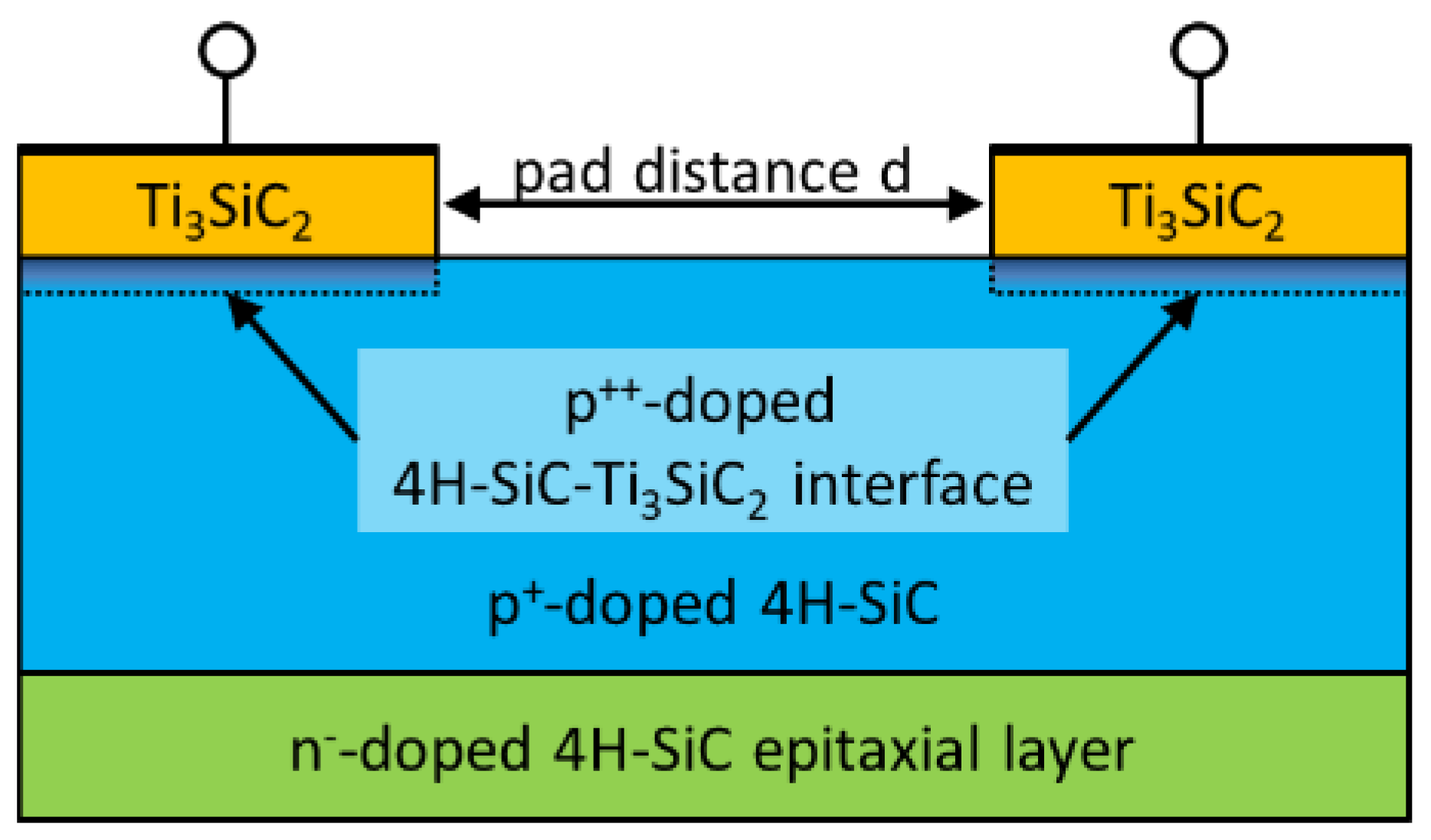
2. Materials and Methods
Transfer length method (TLM) structures with increasing pad distances (30 µm to 480 µm) were fabricated on n− doped 4H-SiC epitaxial layers in order to investigate the contact formation mechanism of Ti/Al based ohmic contact. Al implantation and subsequent high temperature annealing was used to create samples with p+ doped regions and Al surface concentrations between 3.3 × 1018 cm−3 and 5.0 × 1019 cm−3. After depositing and structuring a SiO2 passivation layer, a metal stack consisting of 80 nm Ti and 300 nm Al was deposited and patterned using a lift-off process. Subsequently ohmic contact formation was done by rapid thermal annealing (RTA) at 980 °C in Ar atmosphere. Finally, metal pads for electrical measurements were deposited and structured. A more detailed description of the fabrication process of sample C can be seen elsewhere []. Table 1 gives an overview of the fabricated sets of samples and their fabrication parameters.
Table 1.
Parameters of the fabricated sets of samples.
By using 4-point I-V-measurements (Keithley 4200 Parameter Analyzer, Keithley Instruments, USA) at different temperatures (300 K to 450 K), the fabricated TLM structures were electrically characterized and the sheet resistance , the contact resistance as well as the specific contact resistance were determined in the given temperature range.
Focused ion beam (FIB) (Helios Nanolab 600, FEI, USA) as well as transmission electron microscopy (TEM) analysis were done to determine the thickness of the Ti3SiC2 layer (approx. 100 nm) as well as its stoichiometry.
3. Results
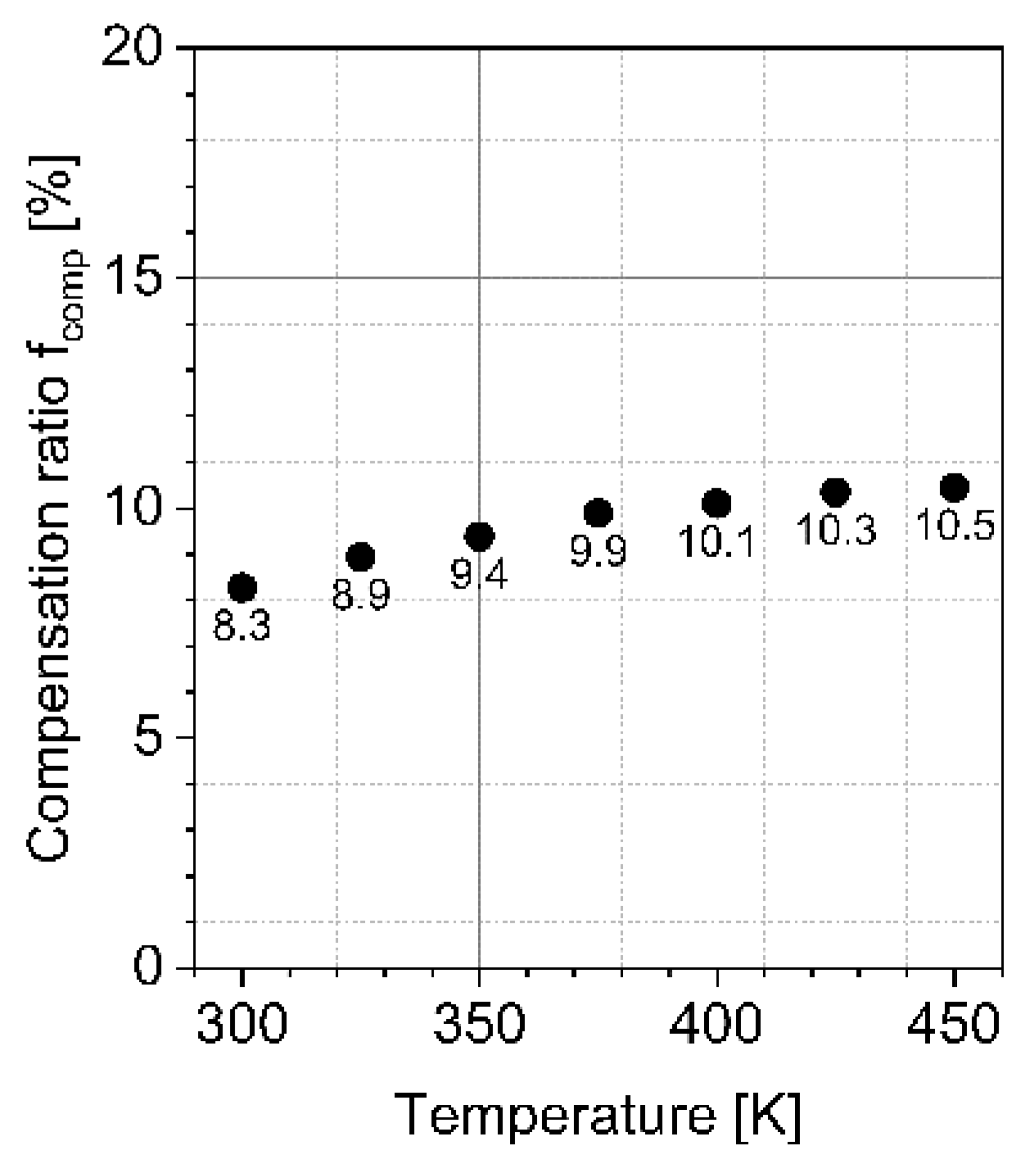
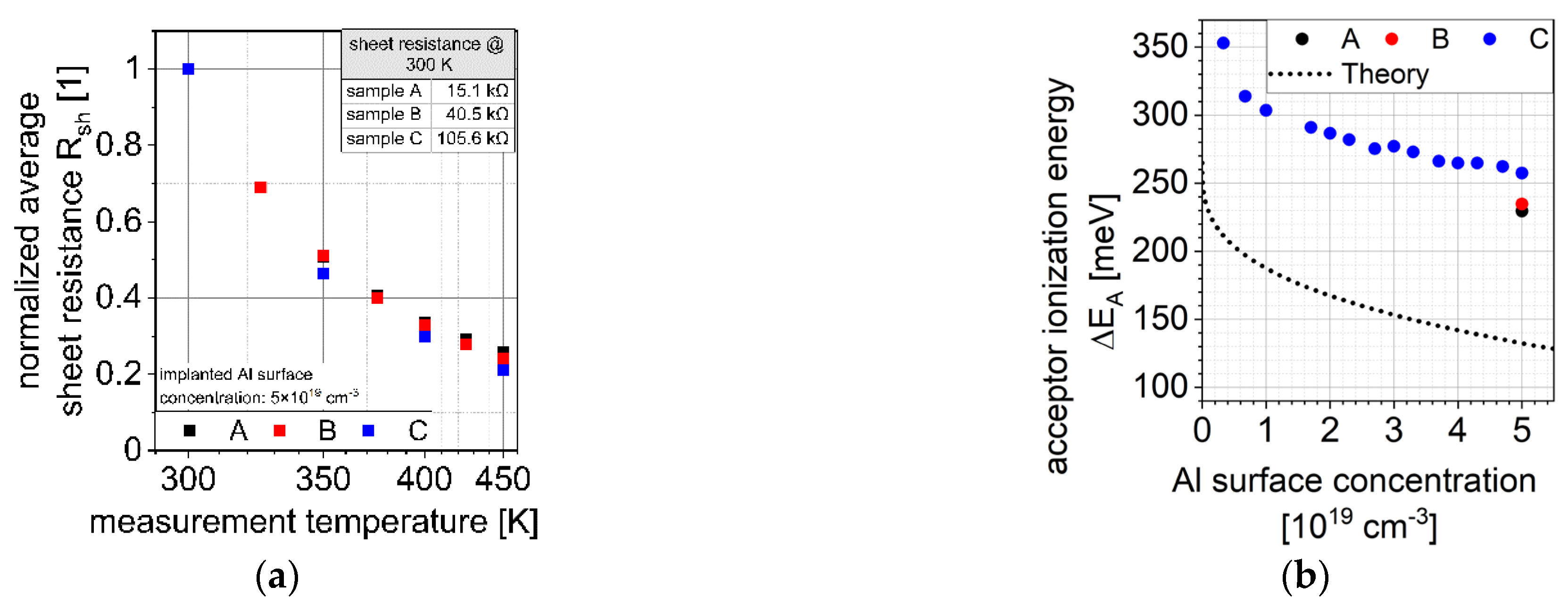
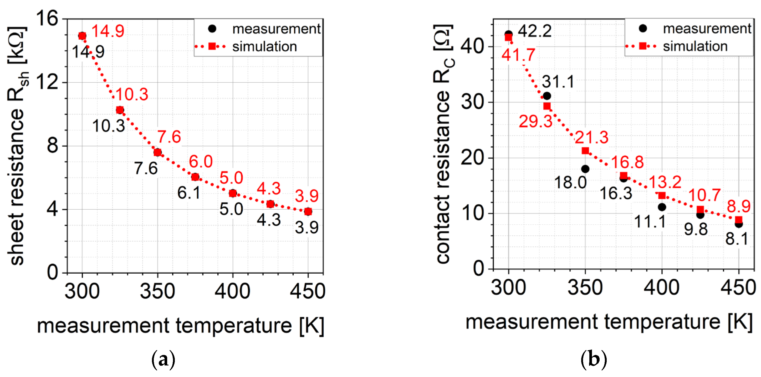
3.1. Sheet Resistance and Determination of the Acceptor Ionization Energy
All fabricated samples show ohmic behavior across all measurement temperatures. The sheet resistance was used to determine the acceptor ionization energies of the fabricated samples. Equation (3) (together with Equations (4)–(8)) can be used to describe the sheet resistance of a semiconductor, where indicates the elementary charge, the thickness of the semiconductor layer, and the hole and electron concentrations, and the hole and electron mobilities, respectively.
Equations (4)–(6) were used to calculate the hole and electron mobility and their respective temperature dependence, where describes the mobility due to phonon scattering, the doping dependent mobility degradation, the temperature, the donor concentration and the acceptor concentration (all other parameters and their values are shown in Table A1 [].
Equations (7) and (8) were used to describe the carrier ionization, where describes the ionized donor concentration and describes the ionized acceptor concentration (all other parameters and their values are shown in Table A2 []. Here, a negligible carrier compensation () was assumed at first.
In Figure 1a the normalized average measured sheet resistances and the associated standard error of all sets of samples with an implanted Al surface concentration of 5 × 1019 cm−3 are shown. It can be seen that all sets of samples show similar temperature dependent behavior despite differences in sheet resistance values (see inset in Figure 1a).
Figure 1.
(a) Measurement temperature dependence of normalized average sheet resistance ; (b) Determined effective acceptor ionization energies .
The associated acceptor ionization energies were determined by fitting the theoretical sheet resistance to the measured ones. The theoretical sheet resistance was determined by using the simulated implantation profile and assuming 100% activation of the dopants.
The determined effective acceptor ionization energies as well as the theoretical acceptor ionization energies (see Equation (9) with = 0.265 eV [,]) are shown in Figure 1b. It can be seen that the determined acceptor ionization energies differ significantly from the theoretical ones, which can be explained by a significant amount of carrier compensation centers (see Equation (8)). As discussed in Section 3.3, these compensation centers might be modelled by donor-like defects that trap free holes.
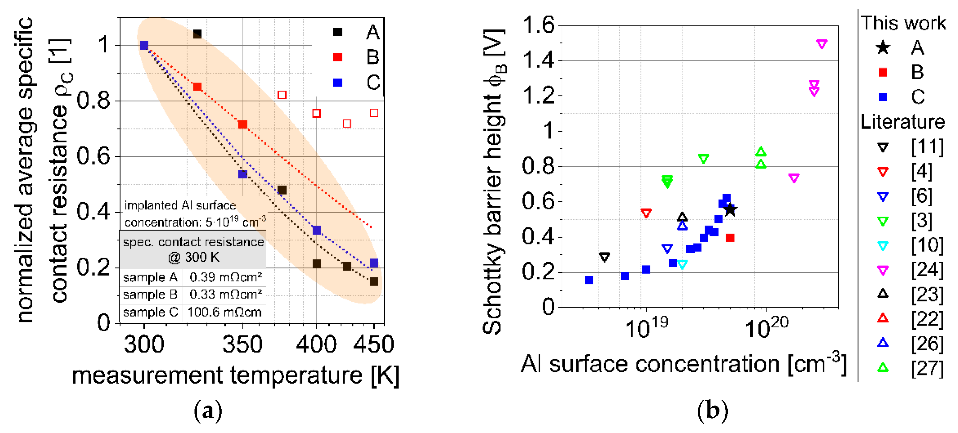
3.2. Determination of Schottky Barrier Height
Based on the Thermionic Field Emission (TFE) model [], Equation (10) can be used to determine the Schottky barrier height , where describes the Boltzmann constant, the Planck constant, the effective tunneling mass (here 0.91 electron masses [,,]), the vacuum permittivity and the relative permittivity of 4H-SiC (here 9.7 [,,]).
The Schottky barrier height itself can be calculated by Equation (11), where describes the bandgap of the semiconductor, the metal workfunction of the ohmic contact material, the electron affinity of the semiconductor and the built-in voltage [,]. It can be seen that the Schottky barrier height decreases slightly with increasing .
Figure 2a shows the normalized average specific contact resistances of all sets of samples with an implanted Al surface concentration of 5 × 1019 cm−3. It can be observed that all sets of samples show quite similar temperature dependent behavior despite different absolute values of the specific contact resistances (see inset of Figure 2a) and despite the deviation of sample B at temperatures higher than 375 K (indicated by the open red squares). The origin of these deviations is not fully understood. Therefore, these values are not used further.
Figure 2.
(a) Normalized average specific contact resistance (b) Determined Schottky barrier heights form this work and literature. Ohmic contacts from literature fabricated on epitaxial regions are indicated with ∇ ([,,,,,]), ohmic contacts from literature fabricated on implanted regions are indicated with Δ ([,,,]).
By fitting the theoretical specific contact resistance to the measured ones, the Schottky barrier heights were determined (see Equation (10)). Figure 2b shows the determined Schottky barrier heights from this work and compares them with Schottky barrier heights known from literature. It can be seen that the determined Schottky barrier heights increase with increasing Al surface concentration, which is in contrast to the theoretically predicted decreasing of the Schottky barrier height with increasing Al surface concentration (see Equation (11)).
In order to investigate this contradiction Secondary Ion Mass Spectrometry (SIMS) analyses were carefully done at the 4H-SiC/Ti3SiC2-interface of sample A by using a CAMECA IMS SC Ultra SIMS tool which allows a sub-nm resolution [,]. The sub-nm depth resolution was achieved for O2+ primary ions with an impact energy of 250 eV. The Al concentration was calibrated using a reference sample consisting of a SiC substrate implanted with Al ions with an energy of 100 keV and a dose of 1014 cm−2.
Figure 3a shows the measured Al concentration, the measured Ti and Si counts per second (CPS) as well as the implanted Al profile. While no Al could be detected in the Ti3SiC2 layer, the Al concentration at the 4H-SiC-Ti3SiC2-interface is significantly increased. This additional Al concentration decreases within approx. 3 nm from a peak concentration of approx. 1021 cm−3 to the implanted Al concentration (5 × 1019 cm−3). Furthermore no significant amount of Ti could be detected in the 4H-SiC layer.
Figure 3.
(a) Measured SIMS profiles of Al, Ti and Si on the Ti3SiC2-SiC interface (b) Approximation of the measured Al profile.
This increase of the Al concentration can be explained by a diffusion of Al during Ti3SiC2 formation. The total resulting Al profile can be approximated by the superposition of the implanted Al profile and the increase of the Al concentration at the 4H-SiC/Ti3SiC2-interface. Equation (12) describes this superposition by using the implanted Al profile , the diffused Al dose during high temperature annealing and the associated diffusion length []. Figure 3b shows the approximation as well as the associated parameters. It can be seen, that the approximation fits very well with the measured data.
3.3. Numerical Simulation
To investigate the influence of the surface-near increased Al concentration as well as the temperature dependent behavior of sample A a numerical simulation model was developed by using Sentaurus TCAD (Version O_2018.06). Figure 4 shows the scheme of the used simulation model. This model includes Ti3SiC2 based ohmic contact pads with a height of 100 nm and a pad distance between the ohmic contacts. The model includes further a homogeneous n−-doped 4H-SiC epitaxial layer, a p+-doped region and a p++-doped region beneath the ohmic contacts. The p+-doped region was created by using a Monte Carlo simulation of the implanted Al profiles. The surface near p++-doped region was created by adding a Gaussian distributed Al profile with diffused Al dose and the associated diffusion length . Furthermore the model assumes complete activation of the Al atoms and takes account of incomplete ionization as well as doping and temperature dependent carrier mobility.
Figure 4.
Scheme of the simulation model.
An additional virtual N profile was added in order to model the concentration of carrier compensation centers. The distribution of this additional virtual N profile is identical with the distribution of the implanted Al profile and can be scaled by using the compensation ratio . Due to these additional donor atoms the concentration of free holes can be reduced similarly to compensation by donor-like traps which increases the associated sheet resistance and allows to fit .
Using this numerical simulation model, I-V characteristics depending on the diffused Al dose , the associated diffusion length and the compensation ratio for each temperature and each pad distance can be obtained. This allows to simulate I-V characteristics for TLM structures at different temperatures.
Based on these I–V characteristics the sheet resistance and the contact resistance of the modelled TLM structures were determined. Figure 5a compares the sheet resistance , Figure 5b compares the contact resistance determined from the electrical measurement data with simulated ones of sample A. It can be seen that both fits are in decent agreement with the measurements. It should be mentioned here that no adjustments on the parameters and determined by the SIMS analysis were necessary.
Figure 5.
(a) Measured and simulated sheet resistance (b) Measured and simulated contact resistance.
The determined compensation ratio is dependent on the temperature as shown in Figure 6. It can be seen that increases slightly with increasing temperature from 8.3% at 300 K to 10.5% at 450 K which fits to temperature independent compensation ratios known from literature (10% to 27%) [,,]. This temperature dependence might be explained by the fact that the ionization energy from nitrogen differs from the ionization energy of the actual compensation centers.
Figure 6.
Temperature dependence of determined compensation ratio.
4. Discussion
Due to the well-fitted simulation results, it can be concluded that the numerical simulation model is suitable to describe Ti3SiC2 based ohmic contacts on p-doped 4H-SiC temperature dependent. Considering the fact that the simulation model does not show ohmic behavior when not using the surface near Al profile it can be further concluded that the surface near Al profile is essential for the ohmic contact formation. Based on these results it is possible to propose a theory regarding the formation mechanism of Ti/Al based ohmic contact on p-doped 4H-SiC and the role of Ti3SiC2 during contact formation.
During the Ti3SiC2 formation a certain amount of Al diffuses in the SiC surface via lattice places and increases the surface near Al concentration significantly. This increase of the surface near Al concentration can significantly decrease the specific resistance (see Equation (10)) and is therefore the key in the ohmic contact formation.
Further investigations are necessary to verify this model and to obtain a better understanding of the conditions leading to the ohmic contact formation under various process conditions. Nevertheless, the fundamental effects are becoming accessible for process integration and process modelling.
Author Contributions
Conceptualization, M.K.; methodology, M.K.; formal analysis, P.P.M.; software, M.K.; writing—original draft preparation, M.K.; writing—review and editing, M.R. and T.E. All authors have read and agreed to the published version of the manuscript.
Funding
This research received no external funding.
Institutional Review Board Statement
Not applicable.
Informed Consent Statement
Not applicable.
Data Availability Statement
The datasets generated and analysed during the current study are available from the corresponding author on reasonable request.
Conflicts of Interest
The authors declare no conflict of interest.
Appendix A
Table A1.
Mobility parameters [].
Table A1.
Mobility parameters [].
| Equation | Parameter | Unit | Electrons | Holes |
|---|---|---|---|---|
| (4) | cm2/Vs | 950 | 125 | |
| (4) | 1 | 2.4 | 2.15 | |
| (5) | cm2/Vs | 40 | 0 | |
| (5) | 1 | −1.536 | −0.57 | |
| (5) | cm2/Vs | 910 | 113.5 | |
| (5) | 1 | −2.397 | −2.6 | |
| (5) | cm−3 | 2.0 × 10¹⁷ | 2.4 × 10¹⁸ | |
| (5) | 1 | 0.75 | 2.9 | |
| (5) | 1 | 0.76 | 0.69 | |
| (5) | 1 | 0.722 | −0.2 |
Table A2.
Incomplete ionization parameters [].
Table A2.
Incomplete ionization parameters [].
| Equation | Parameter | Unit | Nitrogen | Aluminum |
|---|---|---|---|---|
| (7) | 1 | 2 | --- | |
| (7) | eV | 0.0709 | --- | |
| (7) | cm−3 | 1.7193 × 10¹⁹ | --- | |
| (8) | 1 | --- | 4 | |
| (8) | eV | --- | 0.265 | |
| (8) | cm−3 | --- | 1.0752 × 10²⁰ |
References
- Kimoto, T.; Cooper, J.A. Fundamentals of Silicon Carbide Technology: Growth, Characterization, Devices and Applications; IEEE Xplore: Singapore; Piscataway, NJ, USA, 2014; ISBN 978-1-118-31352-7. [Google Scholar]
- Roccaforte, F.; Frazzetto, A.; Greco, G.; Giannazzo, F.; Fiorenza, P.; Lo Nigro, R.; Saggio, M.; Leszczyński, M.; Pristawko, P.; Raineri, V. Critical issues for interfaces to p-type SiC and GaN in power devices. Appl. Surf. Sci. 2012, 258, 8324–8333. [Google Scholar] [CrossRef]
- Abi-Tannous, T.; Soueidan, M.; Ferro, G.; Lazar, M.; Raynaud, C.; Toury, B.; Beaufort, M.-F.; Barbot, J.-F.; Dezellus, O.; Planson, D. A Study on the Temperature of Ohmic Contact to p-Type SiC Based on Ti3SiC2 Phase. IEEE Trans. Electron. Devices 2016, 63, 2462–2468. [Google Scholar] [CrossRef] [Green Version]
- Fisher, C.A. On the Schottky Barrier Height Lowering Effect of Ti3SiC2 in Ohmic Contacts to P-Type 4H-SiC. IJFPS 2014, 4, 95–100. [Google Scholar] [CrossRef]
- Gao, M.; Tsukimoto, S.; Goss, S.H.; Tumakha, S.P.; Onishi, T.; Murakami, M.; Brillson, L.J. Role of Interface Layers and Localized States in TiAl-Based Ohmic Contacts to p-Type 4H-SiC. J. Electron. Mater. 2007, 36, 277–284. [Google Scholar] [CrossRef]
- Jennings, M.R.; Fisher, C.A.; Walker, D.; Sanchez, A.; Pérez-Tomás, A.; Hamilton, D.P.; Gammon, P.M.; Burrows, S.E.; Thomas, S.M.; Sharma, Y.K.; et al. On the Ti3SiC2 Metallic Phase Formation for Robust p-Type 4H-SiC Ohmic Contacts. Mater. Sci. Forum 2014, 778-780, 693–696. [Google Scholar] [CrossRef]
- Johnson, B.J.; Capano, M.A. The effect of titanium on Al–Ti contacts to p-type 4H-SiC. Solid-State Electron. 2003, 47, 1437–1441. [Google Scholar] [CrossRef]
- Johnson, B.J.; Capano, M.A. Mechanism of ohmic behavior of Al/Ti contacts to p-type 4H-SiC after annealing. Solid-State Electron. 2004, 95, 5616–5620. [Google Scholar] [CrossRef]
- Nakatsuka, O.; Takei, T.; Koide, Y.; Murakami, M. Low Resistance TiAl Ohmic Contacts with Multi-Layered Structure for p-Type 4H-SiC. Mater. Trans. 2002, 43, 1684–1688. [Google Scholar] [CrossRef] [Green Version]
- Tang, Y.D.; Shen, H.J.; Zhang, X.F.; Guo, F.; Bai, Y.; Peng, Z.Y.; Liu, X.Y. Effect of Annealing on the Characteristics of Ti/Al Ohmic Contacts to p-Type 4H-SiC. Mater. Sci. Forum 2017, 897, 395–398. [Google Scholar] [CrossRef]
- Tsukimoto, S.; Nitta, K.; Sakai, T.; Moriyama, M.; Murakami, M. Correlation between the electrical properties and the interfacial microstructures of TiAl-based ohmic contacts to p-type 4H-SiC. J. Electron. Mater. 2004, 33, 460–466. [Google Scholar] [CrossRef]
- Tsukimoto, S.; Ito, K.; Wang, Z.; Saito, M.; Ikuhara, Y.; Murakami, M. Growth and Microstructure of Epitaxial Ti3SiC2 Contact Layers on SiC. Mater. Trans. 2009, 50, 1071–1075. [Google Scholar] [CrossRef] [Green Version]
- Ideguchi, K.; Maeda, M.; Takahashi, Y. Nucleation and growth of Ti3SiC2 on SiC by interfacial reaction. IOP Conf. Ser. Mater. Sci. Eng. 2014, 61, 12032. [Google Scholar] [CrossRef] [Green Version]
- Maeda, M.; Takahashi, Y. Formation of Ti3SiC2 on SiC by Control of Interfacial Reaction between SiC and Ti/Al Multilayer. Prepr. Natl. Meet. JWS 2008, 2008, 105. [Google Scholar] [CrossRef]
- Wang, Z.; Tsukimoto, S.; Saito, M.; Ito, K.; Murakami, M.; Ikuhara, Y. Ohmic contacts on silicon carbide: The first monolayer and its electronic effect. Phys. Rev. B 2009, 80, 245303. [Google Scholar] [CrossRef] [Green Version]
- Vivona, M.; Greco, G.; Bongiorno, C.; Lo Nigro, R.; Scalese, S.; Roccaforte, F. Electrical and structural properties of surfaces and interfaces in Ti/Al/Ni Ohmic contacts to p-type implanted 4H-SiC. Appl. Surf. Sci. 2017, 420, 331–335. [Google Scholar] [CrossRef]
- Buchholt, K.; Ghandi, R.; Domeij, M.; Zetterling, C.-M.; Lu, J.; Eklund, P.; Hultman, L.; Spetz, A.L. Ohmic contact properties of magnetron sputtered Ti3SiC2 on n-and p-type 4H-silicon carbide. Appl. Phys. Lett. 2011, 98, 042108. [Google Scholar] [CrossRef]
- Kocher, M.; Rommel, M.; Erlbacher, T.; Bauer, A.J. Influence of Al Doping Concentration and Annealing Parameters on TiAl Based Ohmic Contacts on 4H-SiC. Mater. Sci. Forum 2018, 924, 393–396. [Google Scholar] [CrossRef]
- Synopsys, Inc. Sentaurus™ Device User Guide: Version O-2018.06; Synopsys, Inc.: Mountain View, CA, USA, 2018. [Google Scholar]
- Koizumi, A.; Suda, J.; Kimoto, T. Temperature and doping dependencies of electrical properties in Al-doped 4H-SiC epitaxial layers. J. Appl. Phys. 2009, 106, 13716. [Google Scholar] [CrossRef] [Green Version]
- Sze, S.M.; Ng, K.K.; Ng, K.K. Physics of Semiconductor Devices/Physics of Semiconductor Devices, 3rd ed.; Wiley-Interscience: Hoboken, NJ, USA, 2007; ISBN 0-471-14323-5. [Google Scholar]
- Roccaforte, F.; Vivona, M.; Greco, G.; Lo Nigro, R.; Giannazzo, F.; Di Franco, S.; Bongiorno, C.; Iucolano, F.; Frazzetto, A.; Rascunà, S.; et al. Ti/Al-based contacts to p-type SiC and GaN for power device applications. Phys. Status Solidi A 2017, 214, 1600357. [Google Scholar] [CrossRef]
- Frazzetto, A.; Giannazzo, F.; Lo Nigro, R.; Raineri, V.; Roccaforte, F. Structural and transport properties in alloyed Ti/Al Ohmic contacts formed on p-type Al-implanted 4H-SiC annealed at high temperature. J. Phys. D Appl. Phys. 2011, 44, 255302. [Google Scholar] [CrossRef] [Green Version]
- Thierry-Jebali, N.; Vo-Ha, A.; Carole, D.; Lazar, M.; Ferro, G.; Planson, D.; Henry, A.; Brosselard, P. Very low specific contact resistance measurements made on a highly p-type doped 4H-SiC layer selectively grown by vapor-liquid-solid transport. Appl. Phys. Lett. 2013, 102, 212108. [Google Scholar] [CrossRef] [Green Version]
- Colinge, J.P.; Colinge, C.A. Physics of Semiconductor Devices; Kluwer Academic Publishers: Boston, MA, USA, 2002; ISBN 978-0-306-47622-8. [Google Scholar]
- Roccaforte, F.; Frazzetto, A.; Greco, G.; Lo Nigro, R.; Giannazzo, F.; Leszczyński, M.; Prystawko, P.; Zanetti, E.; Saggio, M.; Raineri, V. Microstructure and Transport Properties in Alloyed Ohmic Contacts to P-Type SiC and GaN for Power Devices Applications. Mater. Sci. Forum 2012, 711, 203–207. [Google Scholar] [CrossRef]
- Zhang, Y.; Guo, T.; Tang, X.; Yang, J.; He, Y.; Zhang, Y. Thermal stability study of n-type and p-type ohmic contacts simultaneously formed on 4H-SiC. J. Alloys Compd. 2018, 731, 1267–1274. [Google Scholar] [CrossRef]
- Michałowski, P.P.; Kozdra, S.; Pasternak, I.; Sitek, J.; Wójcik, A.; Strupiński, W. Precise localization of contaminants in graphene with secondary ion mass spectrometry. Measurement 2021, 110308. [Google Scholar] [CrossRef]
- Michałowski, P.P.; Maciążek, D.; Postawa, Z.; Caban, P.A.; Kozdra, S.; Wójcik, A.; Baranowski, J.M. Defect-mediated sputtering process of boron nitride during high incident angle low-energy ion bombardment. Measurement 2021, 179, 109487. [Google Scholar] [CrossRef]
- Parisini, A.; Nipoti, R. Analysis of the hole transport through valence band states in heavy Al doped 4H-SiC by ion implantation. J. Appl. Phys. 2013, 114, 243703. [Google Scholar] [CrossRef]
- Kocher, M.; Yao, B.T.; Weisse, J.; Rommel, M.; Xu, Z.W.; Erlbacher, T.; Bauer, A. Determination of Compensation Ratios of Al-Implanted 4H-SiC by TCAD Modelling of TLM Measurements. Mater. Sci. Forum 2019, 963, 445–448. [Google Scholar] [CrossRef]
- Weiße, J.; Hauck, M.; Sledziewski, T.; Tschiesche, M.; Krieger, M.; Bauer, A.J.; Mitlehner, H.; Frey, L.; Erlbacher, T. Analysis of Compensation Effects in Aluminum-Implanted 4H-SiC Devices. Mater. Sci. Forum 2018, 924, 184–187. [Google Scholar] [CrossRef]
Publisher’s Note: MDPI stays neutral with regard to jurisdictional claims in published maps and institutional affiliations. |
© 2021 by the authors. Licensee MDPI, Basel, Switzerland. This article is an open access article distributed under the terms and conditions of the Creative Commons Attribution (CC BY) license (https://creativecommons.org/licenses/by/4.0/).