Article

Nondegenerate Polycrystalline Hydrogen-Doped Indium Oxide (InOx:H) Thin Films Formed by Low-Temperature Solid-Phase Crystallization for Thin Film Transistors

1
Materials Science and Engineering Course, Kochi University of Technology, Kami 782-8502, Kochi, Japan
2
Graduate School of Natural Science and Technology, Shimane University, Matsue 690-8504, Shimane, Japan
3
Center for Nanotechnology, Research Institute, Kochi University of Technology, Kami 782-8502, Kochi, Japan
4
Electronic and Photonic Systems Engineering Course, Kochi University of Technology, Kami 782-8502, Kochi, Japan
*
Author to whom correspondence should be addressed.
Materials 2022, 15(1), 187; https://doi.org/10.3390/ma15010187
Submission received: 28 October 2021 / Revised: 2 December 2021 / Accepted: 19 December 2021 / Published: 27 December 2021
(This article belongs to the Special Issue Advanced Semiconductor Materials and Devices 2021)

Abstract

:
We successfully demonstrated a transition from a metallic InOx film into a nondegenerate semiconductor InOx:H film. A hydrogen-doped amorphous InOx:H (a-InOx:H) film, which was deposited by sputtering in Ar, O2, and H2 gases, could be converted into a polycrystalline InOx:H (poly-InOx:H) film by low-temperature (250 °C) solid-phase crystallization (SPC). Hall mobility increased from 49.9 cm2V−1s−1 for an a-InOx:H film to 77.2 cm2V−1s−1 for a poly-InOx:H film. Furthermore, the carrier density of a poly-InOx:H film could be reduced by SPC in air to as low as 2.4 × 1017 cm−3, which was below the metal–insulator transition (MIT) threshold. The thin film transistor (TFT) with a metallic poly-InOx channel did not show any switching properties. In contrast, that with a 50 nm thick nondegenerate poly-InOx:H channel could be fully depleted by a gate electric field. For the InOx:H TFTs with a channel carrier density close to the MIT point, maximum and average field effect mobility (μFE) values of 125.7 and 84.7 cm2V−1s−1 were obtained, respectively. We believe that a nondegenerate poly-InOx:H film has great potential for boosting the μFE of oxide TFTs.

1. Introduction

Transparent metal oxide semiconductors (OSs) have been extensively investigated for use as the active channel layer of thin film transistors (TFTs) for next-generation flat-panel displays [1,2,3], nonvolatile memories [4,5], image sensors [6,7], and pH sensors [8,9], to name a few. Among OSs, the amorphous In–Ga–Zn–O (IGZO) [10] has attracted particular attention for TFT applications owing to its high field effect mobility (μFE) of more than 10 cm2V−1s−1, steep subthreshold swing (S.S.), extremely low off-state current, large-area uniformity, and good bias stress stability [11]. Although the μFE of an IGZO TFT is approximately one order of magnitude higher than that of an amorphous Si TFT, further improvement of the μFE of OS TFTs is required to expand their range of applications as an alternative to polycrystalline Si TFT.
Single-crystalline In2O3 has a Hall mobility as high as 160 cm2V−1s−1 [12], which makes amorphous (a-) or polycrystalline (poly-) InOx a potential material for enhancing the μFE of OS TFTs. However, it is known that undoped InOx thin films exhibit a high background electron density, which is attributed to the presence of native defects, such as oxygen vacancies, making them unsuitable for a channel material of OS TFTs. To reduce the background carrier density, a small amount of a carrier suppressor, having a high bond dissociation energy with oxygen, such as W, Si, or Ti, is doped into an a-InOx thin film [13,14]. μFE values of 32, 30, and 17 cm2V−1s−1 were reported for the TFTs with a-InOx:Ti, W, and Si channels, respectively [13]. An atomic layer deposition (ALD) method is also used to form a- or poly-InOx channels for TFTs [15,16,17,18]. The TFT with a 5 nm thick ALD-deposited carbon-doped a-InOxchannel with μFE of 20.4 cm2V−1s−1 has been demonstrated [18]. Higher μFE values of 39.2 and 41.8 cm2V−1s−1 were reported for the TFTs with ultrathin (5 nm) poly-InOx channels formed by plasma- or ozone-assisted ALD followed by postdeposition annealing (PDA). [15,16], A poly-InOx film is also known to be deposited by sputtering even without substrate heating. A fully depleted poly-InOx TFT with μFE of 15.3 cm2V−1s−1 was obtained by decreasing the channel thickness to 8 nm. [19] Most a- and poly-InOx TFTs have been demonstrated with an ultrathin (<10 nm) channel layer [13,14,15,16,18,19], in order to fully deplete degenerate InOx channels. However, an ultrathin poly-InOx channel layer limits the μFE of the TFTs, since the grain size of the film is small. Poly-InOx films have also been investigated for use as the transparent conductive oxide (TCO) in solar cells. Koida et al. [20,21,22,23,24,25] reported a hydrogen-doped poly-InOx (InOx:H) film with high electron mobility and high near-infrared (NIR) transparency prepared by solid-phase crystallization (SPC) [20]. To incorporate H-donors into InOx, H2O vapor or H2 gas is introduced during sputtering deposition. During the PDA of an InOx:H film, phase transition from amorphous to polycrystalline (SPC) occurred at ~175 °C. The SPC poly-InOx:H films showed a Hall mobility as high as 100–130 cm2V−1s−1; however, its carrier density (>1 × 1020 cm−3) was too high to apply it as a channel layer of the TFT [20]. Thus, for the TFT application, the carrier density should be reduced to obtain a nondegenerate semiconductor InOx:H film. We previously reported the electrical properties of the H-doped a-IGZO (IGZO:H) prepared by sputtering in Ar, O2, and H2 gases [26,27,28,29]. Although the as-deposited IGZO:H was degenerate semiconductor with the carrier density of over 1 × 1020 cm−3, carrier density significantly decreased more than two orders of magnitude after PDA at 150 °C in air.
In this work, nondegenerate poly-InOx:H thin films were successfully prepared by SPC. A degenerate a-InOx:H thin film was deposited by sputtering in Ar, O2, and H2 gases, and an amorphous to polycrystalline phase transition of the film was achieved after PDA at more than 175 °C. By PDA at 250 °C in air, a nondegenerate poly-InOx:H film could be obtained with a carrier density as low as 2.4 × 1017 cm−3, which is approximately three orders of magnitude lower than that of the initial a-InOx:H film. The TFTs with a 50 nm thick nondegenerate InOx:H channel could be fully depleted by a gate electric field. A maximum μFE of 125.7 cm2V−1s−1 was exhibited by the TFT with the poly-InOx:H channel. The use of a nondegenerate poly-InOx:H film is a promising approach to boost the μFE of OS TFTs.

2. Experiments

Indium oxide (InOx) and hydrogenated InOx (InOx:H) films with a thickness of 50 nm were deposited on a glass substrate by radio frequency (RF) magnetron sputtering, without intentional substrate heating, from a ceramic In2O3 target. Mixed gases of Ar/O2 and Ar/O2/H2 were used for depositing InOx and InOx:H films, respectively. The O2 gas flow ratio, which was defined as R[O2] = O2/(Ar + O2+ H2), was set at 4% for both films, while the H2 gas flow ratio, which was defined as R[H2] = H2/(Ar + O2 + H2), was set at 1, 5, and 9% for InOx:H films. All the films were deposited at 0.4 Pa and then annealed at temperatures ranging from 100 to 400 °C in either N2 or ambient air. The carrier concentration (Ne) and Hall mobility (μH) of the films were measured by Hall effect measurements using van der Pauw geometry. An absorption coefficient (α) of the films was evaluated from transmittance and reflectance measurements. The crystallinity and grain size of the films were evaluated by X-ray diffraction (XRD) analysis and scanning electron microscopy (SEM), respectively. The amounts of hydrogen and hydroxyl groups in the films were measured by thermal desorption spectroscopy (TDS). The chemical composition (In/O ratio) and hydrogen content in the films were measured by Rutherford backscattering spectrometry (RBS) and elastic recoil detection analysis (ERDA), respectively. The chemical bonding states of the films were evaluated by a custom-made, hard X-ray photoelectron spectroscopy (HXPS) system with a CrKα X-ray source of 5415 eV and a wide acceptance angle electron analyzer.

3. Results and Discussion

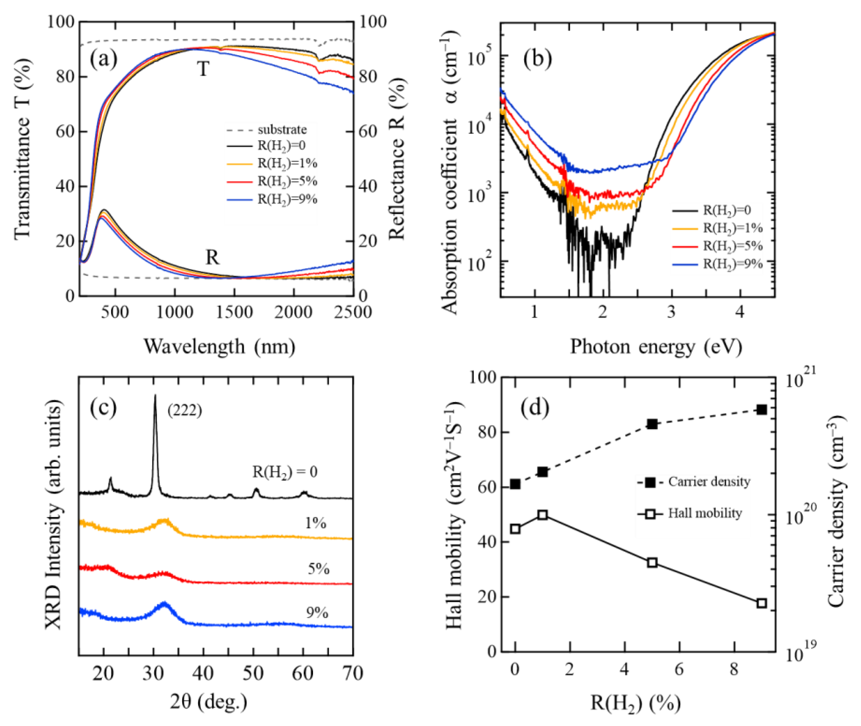
3.1. Optical, Electrical, and Structural Properties of As-Deposited InOx and InOx:H Films

Figure 1a shows the transmittance and reflectance of the as-deposited InOx and InOx:H films. The absorption edge of the InOx:H films shifted to a shorter wavelength as R(H2) increased. On the other hand, the transmittance of the InOx:H films decreased in the NIR region with increasing R(H2). Figure 1b shows the absorption coefficient (α) of the as-deposited InOx and InOx:H films as a function of photon energy. The subgap α of the InOx:H films increased with R(H2). Figure 1c shows XRD spectra of the as-deposited InOx and InOx:H films. An InOx film showed a clear polycrystalline nature with a (222) preferred orientation, whereas all the InOx:H films with R(H2) from 1 to 9% exhibited an amorphous nature. These results indicate that added H2 suppressed crystallization in the vapor phase during the deposition and formed the a-InOx:H film. Figure 1d shows the μH and Ne of the as-deposited poly-InOx and a-InOx:H films as a function of R(H2), during the deposition. The poly-InOx film showed μH of 44.8 cm2V−1s−1. On the other hand, the μH of a-InOx:H film increased to 49.9 cm2V−1s−1 at R(H2) of 1%; however, it decreased to 17.7 cm2V−1s−1 as R(H2) further increased to 9%. Since hydrogen acts as a shallow donor in the films, Ne monotonically increased from 1.7 × 1020 cm−3 for poly-InOx to 5.8 × 1020 cm−3 for a-InOx:H, upon R(H2) increasing to 9%. Thus, the transmittance of the a-InOx:H films decreased in the NIR region owing to a free carrier absorption. The increases in subgap α and Ne, and the decrease in the μH of the as-deposited a-InOx:H films suggest that H2 added during film deposition generates defects such as oxygen vacancies (VO), owing to sputtering in a reducing atmosphere.

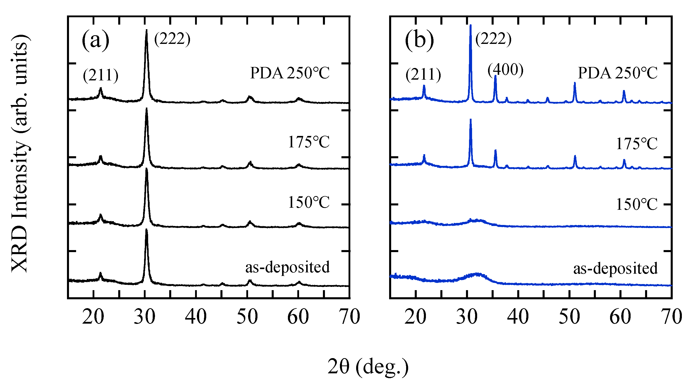
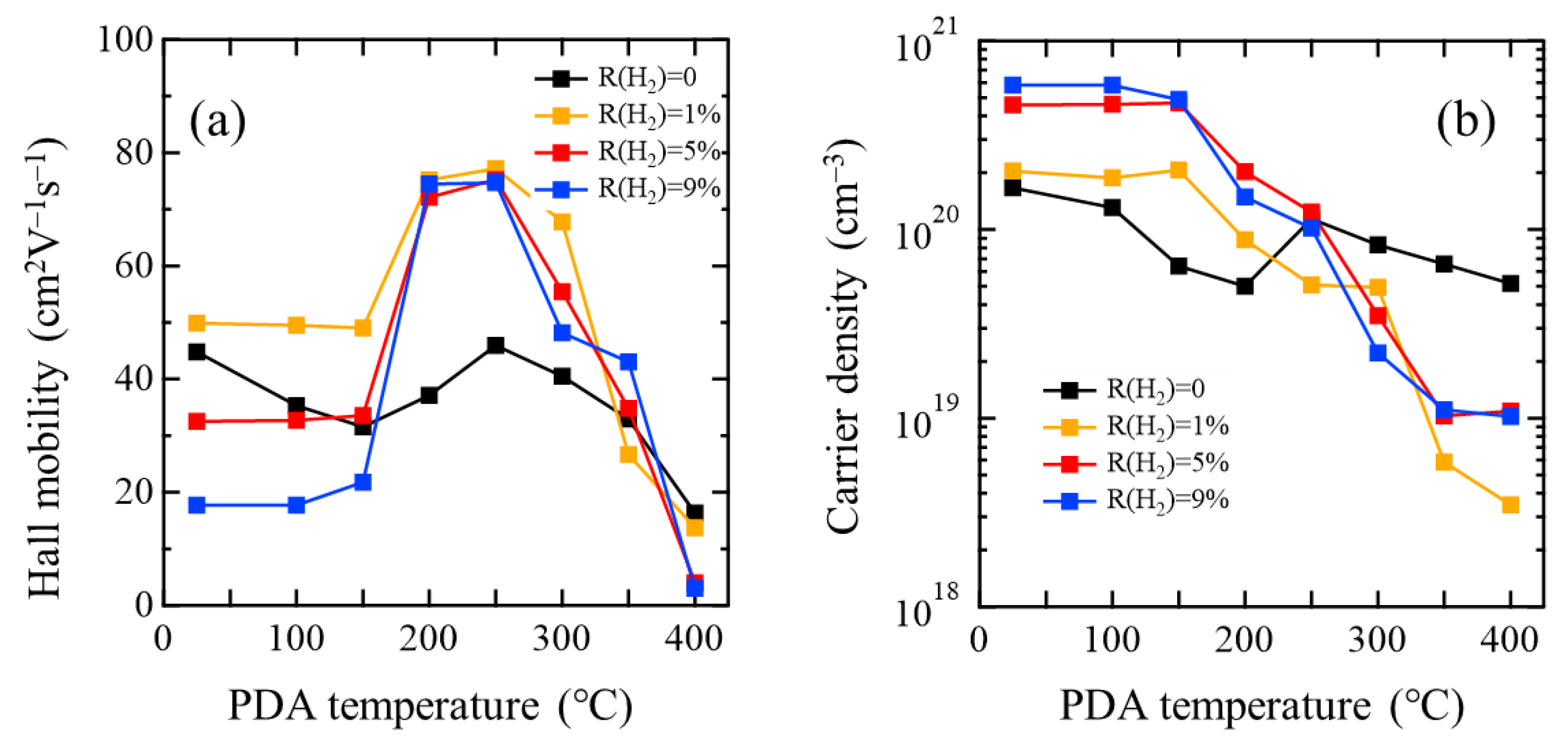
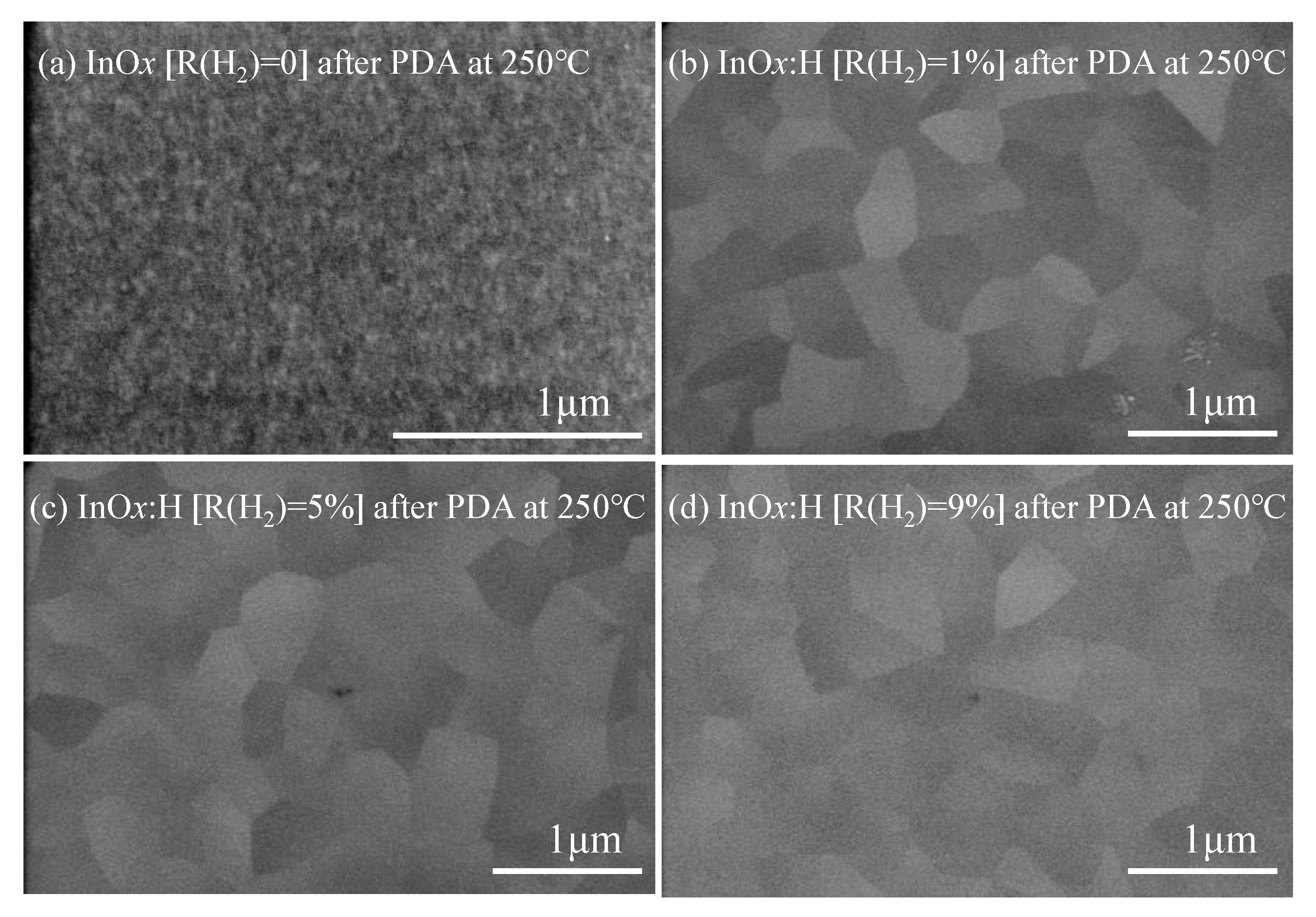
3.2. Changes in Film Properties through PDA

Figure 2 shows XRD spectra of (a) InOx and (b) InOx:H [R(H2) of 5%] films before (as-deposited) and after PDA at 150, 175, and 250 °C for 1 h. An InOx film showed a clear polycrystalline nature with a (222) preferred orientation even before annealing (as-deposited), whereas the InOx:H film remained amorphous even after PDA at 150 °C. The a-InOx:H film could be converted to a poly-InOx:H film when the PDA temperature was raised to more than 175 °C. In this paper, we define the amorphous to polycrystalline phase transition upon PDA as SPC. In addition, the full width at half maximum (FWHM) of the poly-InOx:H film was smaller than that of the poly-InOx film after PDA at 250 °C (data not shown here), indicating a higher crystallinity of the poly-InOx:H film than of the poly-InOx film. The In/O ratio of the films after PDA at 250 °C were 0.51 for poly-InOx film and 0.55 poly-InOx:H film, indicating that both films contain higher O content than the stoichiometric film (In/O ratio of 0.67). The atomic ratio of hydrogen in the poly-InOx:H film was estimated to be 8.6% after the SPC process at 250 °C.
Figure 3 shows SEM views of the poly-InOx and poly-InOx:H film surfaces after PDA at 250 °C. The poly-InOx film showed very fine grains. In contrast, the grain size of the poly-InOx:H film significantly increased to ~400 nm, owing to SPC from the a-InOx:H film. Moreover, the grain size of the poly-InOx:H film did not depend on R(H2).
Figure 4 shows (a) μH and (b) Ne values of the InOx and InOx:H films as a function of the temperature of the PDA, which was applied in N2 for 1 h. μH of the poly-InOx film (without H2) after PDA at 250 °C was 46.0 cm2V−1s−1, which was almost unchanged from that of the as-deposited InOx film. In contrast, the μH of all the InOx:H films sharply increased after PDA at 200 °C, which is in good agreement with the phase transition temperature from amorphous to polycrystalline, as shown in Figure 2b. Furthermore, all the poly-InOx:H films with R(H2) values of 1, 5, and 9% exhibited almost the same μH because their grain sizes were almost the same, as shown in Figure 3. Thus, the enlargement of the grain size and the improvement of intragrain crystallinity due to SPC are the main causes of the improved μH of the poly-InOx:H films after PDA at 200 °C. Maximum μH values of 74.8–77.2 cm2V−1s−1 were obtained from the poly-InOx:H films after PDA at 250 °C. On the other hand, the Ne values of as-deposited poly-InOx and a-InOx:H [R(H2) of 9%] films were 1.7 × 1020 cm−3 and 5.8 × 1020 cm−3, respectively. Although the Ne of the films slightly decreased after PDA at 250 °C, all the poly-InOx:H films were still degenerate with Ne values of 5.1 × 10¹⁹–1.2 × 1020 cm−3.
Since Ne values of N2-annealed poly-InOx and poly-InOx:H films are too high for these films to be used as a channel layer of the TFT, the annealing ambient was changed from N2 to air to reduce the Ne of the films. Figure 5a shows the Ne values of the as-deposited and 250 °C annealed poly-InOx and InOx:H films as a function of R(H2) during film deposition. As mentioned previously, the Ne of as-deposited films increased with R(H2). After PDA at 250 °C in N2 (same as shown in Figure 4b), all the films showed mostly the same Ne of approximately 1020 cm−3, regardless of R(H2). On the other hand, after PDA at 250 °C in air, the Ne of the InOx film decreased to 2.8 × 1019 cm−3, while those of the poly-InOx:H films further decreased from 1.4 × 1018 cm−3 to 2.7 × 1017 cm−3 as R(H2) increased from 1 to 9%. The Ne of the poly-InOx:H films annealed in air decreased by more than two orders of magnitude from that of the films annealed in N2. This result indicates that both the H2 added during the film deposition and the oxygen in the annealing ambient play an important role in reducing the Ne of the films. The Hall measurement results presented in Figure 5a are also summarized in Table 1.
The critical carrier density of the metal–insulator transition (MIT) is given by the Mott criterion nc = (0.26/aH)3, where aH denotes the effective Bohr radius of a hydrogenic donor [29]. For In2O3 with a relative dielectric constant (ε) of 9, nc is calculated to be 1.6 × 10¹⁸–7.2 × 1018 cm−3 when the electron effective mass (m*/m0) is assumed to be 0.1–0.3 [30,31,32]. Thus, a nondegenerate semiconductor film would be obtained from the InOx:H films.
Figure 5b shows the inverse temperature (1000/T) dependence of the resistivity (ρ) of the films after PDA at 250 °C in air. For the poly-InOx film [R(H2) = 0], ρ did not change in the temperature range from 100 to 300 K, indicating that the film exhibited degenerate metallic conduction. On the other hand, the ρ of the poly-InOx:H with R(H2) of 1% increased from 1.7 × 10⁻² to 5.1 × 10⁻² Ω·cm when the measurement temperature was decreased from 300 to 100 K. The positive correlation of ρ and inverse temperature further increased for the films with R(H2) values of 5 and 9%. This result clearly indicated that nondegenerate semiconductor poly-InOx:H films could be obtained by SPC in air.

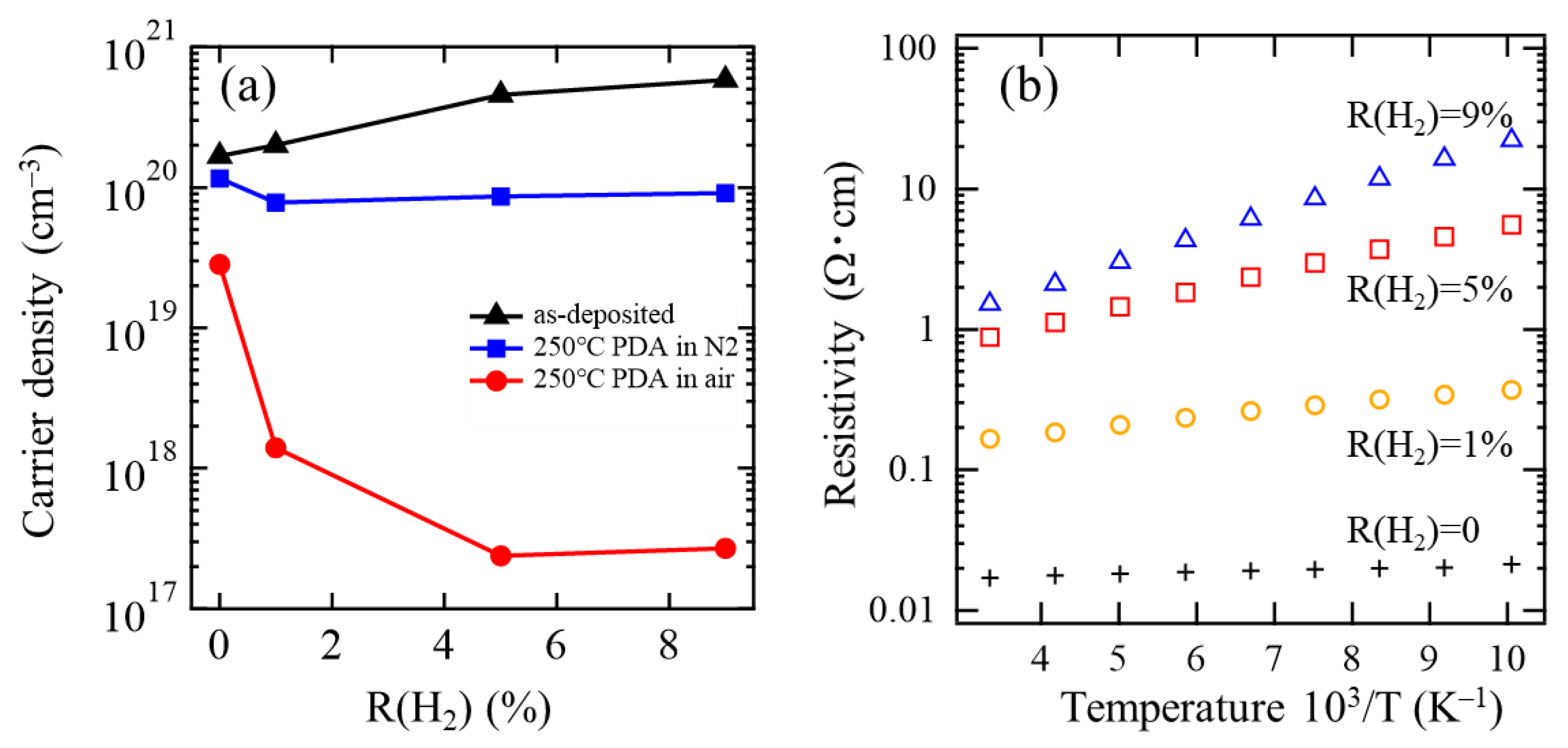
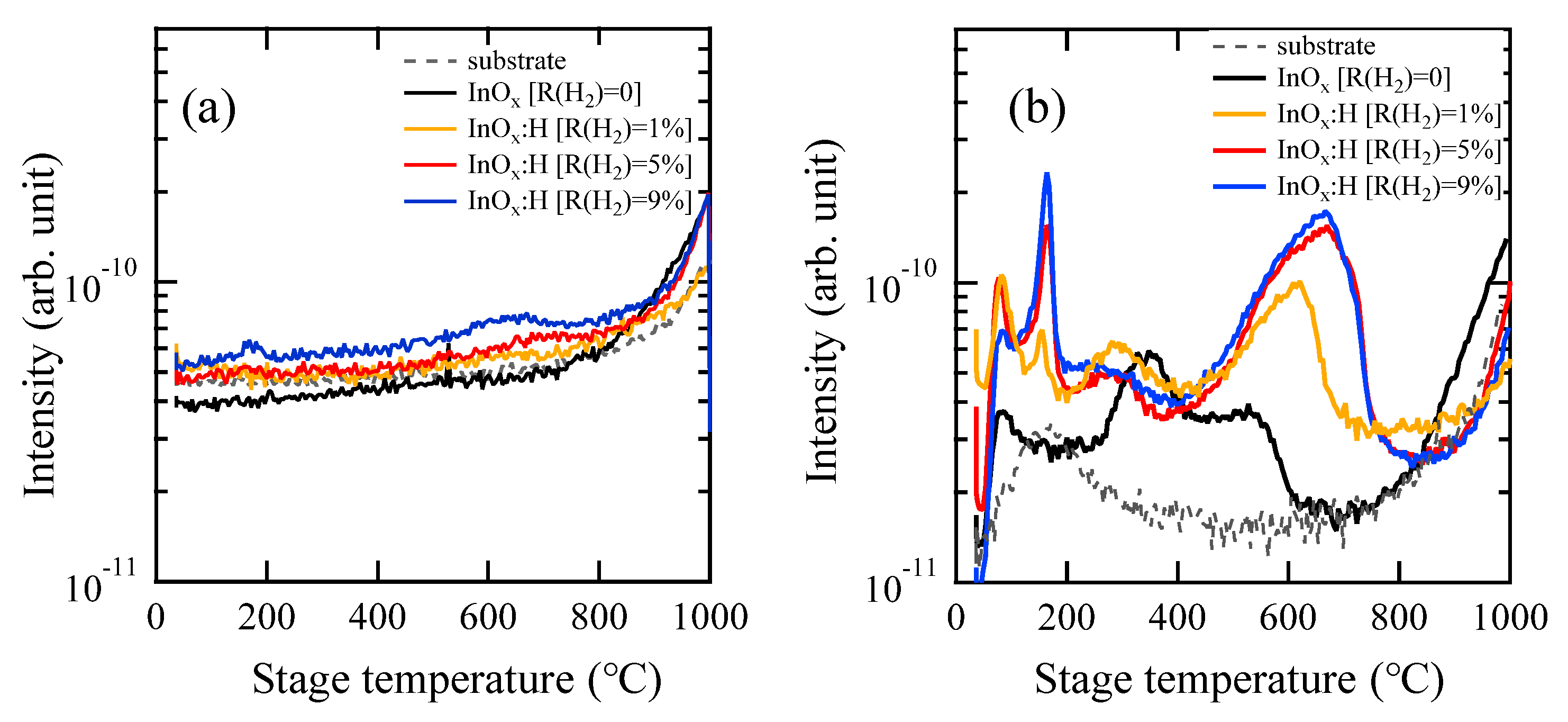
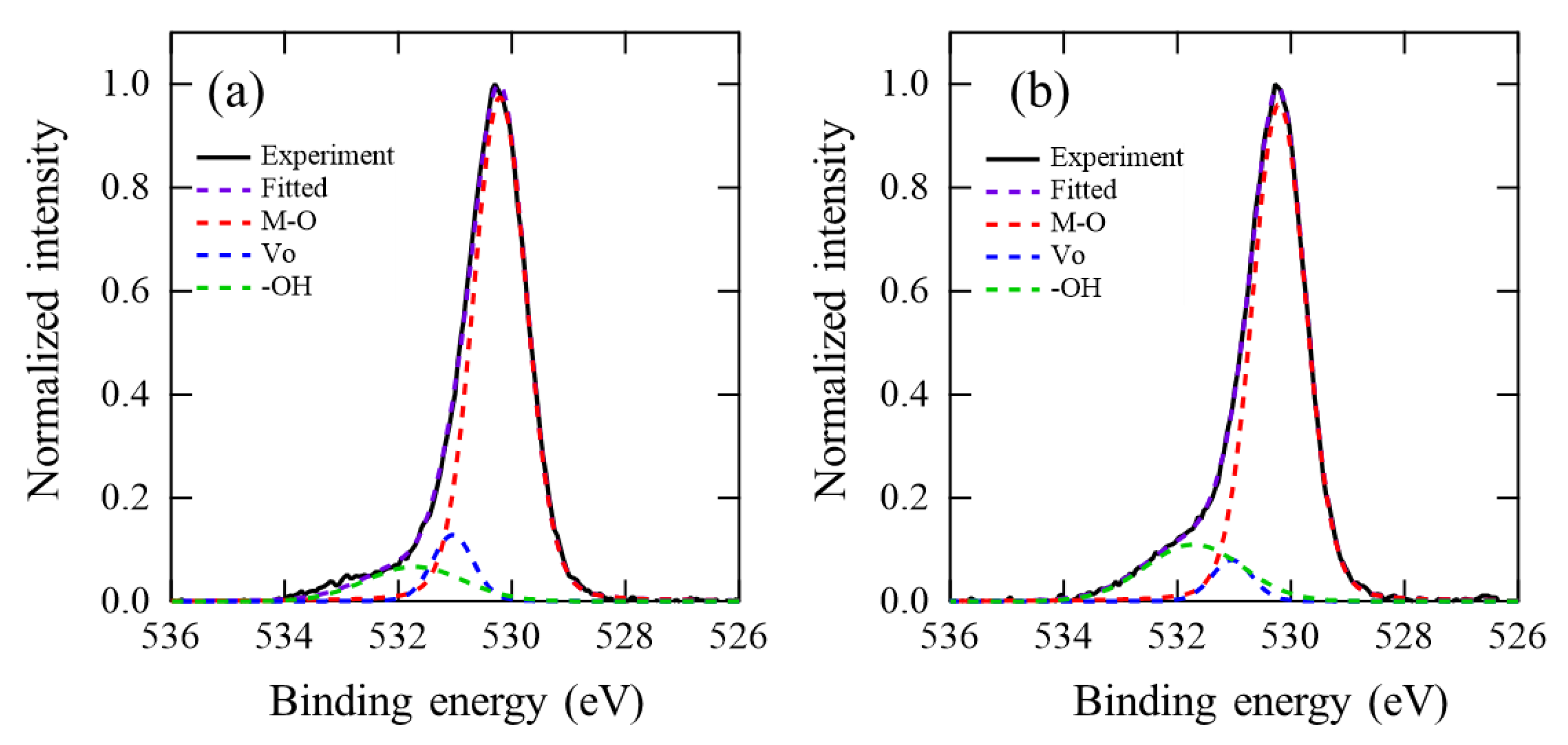
3.3. TDS and HXPS Analysis of InOx and InOx:H Films

An introduced H2 in the InOx:H films was evaluated by a thermal desorption spectroscopy (TDS). Figure 6 presents TDS spectra of mass-to-charge ratios (m/z) of (a) 2 (H2) and (b) 18 (H2O) obtained from the as-deposited poly-InOx and a-InOx:H films. No clear desorption peak of H2 was observed from either the InOx or InOx:H film, whereas several H2O desorption peaks were observed from both types of film, indicating that the introduced H2 exists within the hydroxyl (–OH) bonds in the InOx:H films. The first H2O desorption peak due to adsorbed H2O molecules at the sample surface was observed at around 80 °C. The second H2O desorption peak at around 165 °C was observed only from the InOx:H films and is attributed to the desorption of hydroxyl (–OH) bonds in the films during an amorphous to polycrystalline phase transition. We also confirmed a small amount of argon desorption from the InOx:H films at the same temperature as the second peak (data not shown) [21]. The H2O desorption observed at a temperature higher than 250 °C can be attributed to the remaining −OH bonds in the films after PDA at 250 °C. TDS results indicated that the number of remained −OH bonds in the InOx:H film increased as R(H2) increased from 1 to 5%, and it saturated at R(H2) values of 5 and 9%.
Figure 7 shows O 1s HXPS spectra obtained from (a) poly-InOx and (b) poly-InOx:H (R[H2] = 5%) films after PDA at 250 °C, respectively. The O 1s spectra were well fitted by three Gaussian–Lorentz curves at 530.2, 531.0, and 531.7 eV, attributed to the metal–oxygen bonds (M–O), oxygen vacancies (VO), and oxygen in the hydroxides (−OH), respectively [29]. The relative area ratio of −OH increased from 9.7% for poly-InOx film to 15.8% for poly-InOx:H film, whereas that of VO reduced from 8.2% for poly-InOx film to 5.0% for poly-InOx:H film. The HXPS result clearly revealed that hydrogen remained in poly-InOx:H film as −OH bonds and reduced VO in the film.
By comparing the TDS and HXPS results of the remaining −OH bonds and the Ne of the InOx:H films, as shown in Figure 5a, we conclude that the remaining −OH bonds in the film after PDA play an important role in the passivation of oxygen vacancies, which results in the decreasing Ne of the InOx:H film.

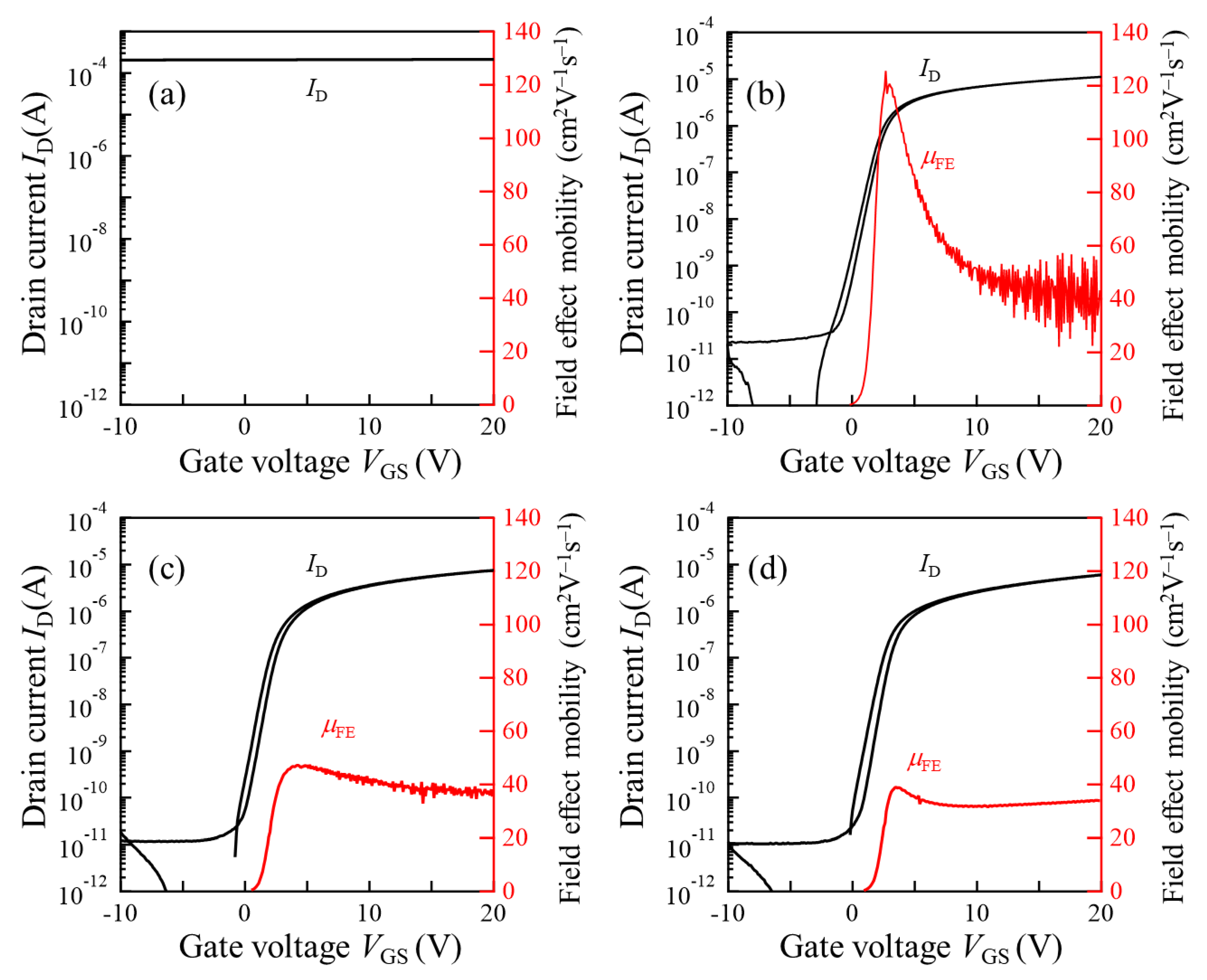
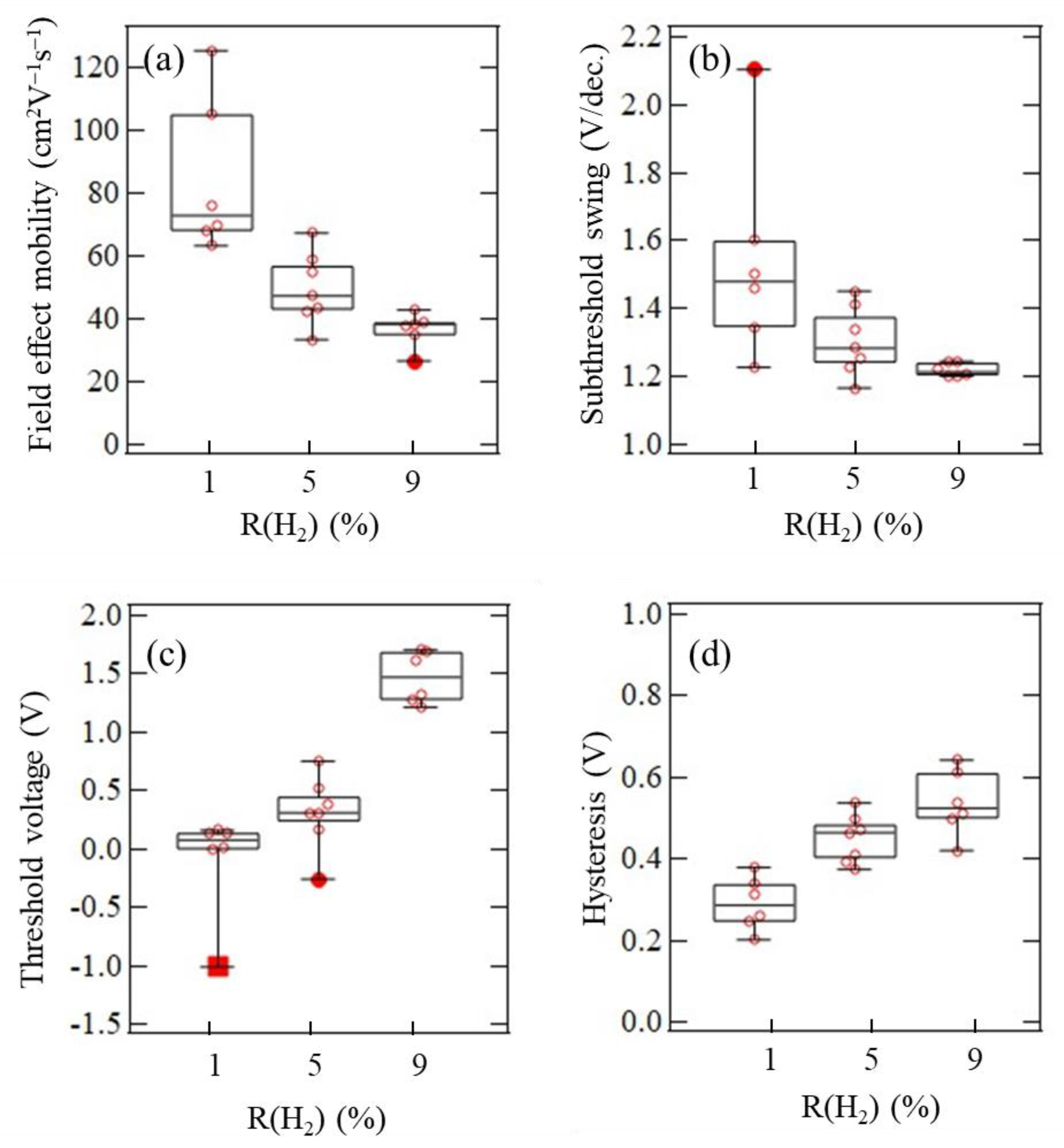
3.4. TFT Application of Polycrystalline InOx and InOx:H Films

Bottom-gate poly-InOx and poly-InOx:H TFTs were fabricated on a heavily doped n+-Si substrate with a 100 nm thick thermally grown SiO2 (th-SiO2) layer. The Si substrate and th-SiO2 were used as the gate electrode and gate insulator (GI) for the TFTs, respectively. The 50 nm thick poly-InOx and a-InOx:H films were deposited by sputtering on a GI as a channel layer using a metal mask. R(O2) was set at 4% for both films, while R(H2) was set at 1, 5, and 9% for the a-InOx:H film. After the deposition, PDA was applied in both films at 250 °C for 1 h in air. Source and drain electrodes of Au were formed by vacuum evaporation using a metal mask. Finally, TFTs were post-annealed at 200 °C for 1 h in air. The channel length and width of the TFTs were 1000 and 350 μm, respectively.
Figure 8 shows transfer characteristics of the TFTs with poly-InOx and poly-InOx:H channels. The field effect mobility (μFE) was extracted from the linear region with a drain voltage of 0.1 V. The gate leakage current of all the TFTs at a gate voltage of 20 V was below 0.1 nA (data not shown), which was approximately 5 orders of magnitude lower than the drain current. Thus, gate leakage current had no effect on the extraction of the μFE. The TFT with a poly-InOx channel did not show switching properties, as shown in Figure 7a. Since the poly-InOx film exhibited degenerate metallic conduction with Ne of 2.8 × 1019 cm−3, a 50 nm thick channel could not be fully depleted by the gate electric field. In contrast, all the TFTs with poly-InOx:H channels showed clear switching properties. This result indicated that the penetration depth of the gate electric field significantly increases in the nondegenerate poly-InOx:H channel upon the transition from metal to semiconductor; thus, the 50 nm thick poly-InOx:H channels could be fully depleted by the gate electric field.
Figure 9 and Table 2 show the variations of the TFT properties evaluated for seven TFTs on the same substrate. From the poly-InOx:H TFTs with R(H2) of 1% and Ne close to the critical carrier density of the MIT point, the maximum and average μFE values of 125.7 and 84.7 cm2V−1s−1 were obtained, respectively. Since a hump was often observed in the subthreshold region of high-μFE TFTs, the variation of a subthreshold swing (S.S.) also increased for the TFTs with R(H2) of 1%. When R(H2) increased, although the average μFE decreased to 49.7 cm2V−1s−1 and 37.0 cm2V−1s−1 for the TFTs with R(H2) values of 5% and 9%, respectively, S.S. and its variation became better. In addition, threshold voltage (Vth) shifted positively, but hysteresis (VH) increased as R(H2) increased.
Although further optimization of TFTs and understanding of the role of hydrogen on electrical properties and reliability are still necessary, we successfully demonstrated the formation of high-μFE TFTs with a nondegenerate poly-InOx:H channel, formed by SPC. We believe that a nondegenerate polycrystalline InOx:H channel has great potential for boosting the μFE of oxide TFTs.

4. Conclusions

In this paper, nondegenerate poly-InOx:H thin films were formed by low-temperature SPC. An a-InOx:H film deposited by sputtering in Ar, O2, and H2 gases could be converted to a poly-InOx:H film by SPC at 250 °C. Hall mobility increased from 49.9 cm2V−1s−1 for an a-InOx film to 77.2 cm2V−1s−1 for a poly-InOx:H film. Furthermore, we successfully demonstrated a transition from a metallic poly-InOx film to a nondegenerate semiconductor poly-InOx:H film. The carrier density of the poly-InOx:H film could be reduced to as low as 2.4 × 1017 cm−3, which was more than two orders of magnitude lower than that of the poly-InOx film (1.7 × 1020 cm−3). The TFT with a metallic poly-InOx channel did not show any switching properties; in contrast, a 50 nm thick nondegenerate InOx:H channel was fully depleted by a gate electric field. For the InOx:H TFTs with a channel carrier density close to the critical carrier density of the MIT point, maximum and average μFE values of 125.7 and 84.7 cm2V−1s−1 were obtained, respectively. We believe that a nondegenerate polycrystalline InOx:H channel has great potential for boosting the μFE of oxide TFTs.

Author Contributions

Conceptualization, M.F.; methodology, T.K., Y.M. and M.F.; validation, T.K. and Y.M.; formal analysis, T.K., Y.M. and H.M.; investigation, T.K., Y.M.; resources, M.F. and H.M.; data curation, T.K., Y.M., H.M. and M.F.; writing—original draft preparation, T.K. and M.F.; writing—review and editing, M.F.; visualization, T.K. and Y.M.; supervision, M.F.; project administration, M.F. All authors have read and agreed to the published version of the manuscript.

Funding

This research received no external funding.

Data Availability Statement

The data presented in this study are available on request from the corresponding author.

Acknowledgments

The authors would like to thank F. Nishiyama, Hiroshima University, Japan for his contribution to the RBS and ERDA analyses, which were supported by the “Nanotechnology Platform” (Project No. F-21-RO-0033) of the Ministry of Education, Culture, Sports, Science and Technology (MEXT), Japan.

Conflicts of Interest

The authors declare no conflict of interest.

References

  1. Ito, M.; Kon, M.; Ishizaki, M.; Sekine, N. Flexible Active-Matrix TFT Array with Amorphous Oxide Semiconductors for Electronic Paper. In Proceedings of the Display Workshops in Conjunction with Asia Display 2005 (IDW/AD’05), Takamatsu, Japan, 6–9 December 2005; p. 845. [Google Scholar]
  2. Hirao, T.; Furuta, M.; Furuta, H.; Matsuda, T.; Hiramatsu, T.; Hokari, H.; Yoshida, M. 4.1: Distinguished Paper: High Mobility Top-Gate Zinc Oxide Thin-Film Transistors (ZnO-TFTs) for Active-Matrix Liquid Crystal Displays. SID Symp. Dig. Tech. Pap. 2006, 37, 18–20. [Google Scholar] [CrossRef]
  3. Park, S.-H.K.; Hwang, C.-S.; Lee, J.-I.; Chung, S.M.; Yang, Y.S.; Do, L.-M.; Chu, H.Y. 4.3: Transparent ZnO Thin Film Transistor Array for the Application of Transparent AM-OLED Display. SID Symp. Dig. Tech. Pap. 2006, 37, 25–28. [Google Scholar] [CrossRef]
  4. Inoue, H.; Matsuzaki, T.; Nagatsuka, S.; Okazaki, Y.; Sasaki, T.; Noda, K.; Matsubayashi, D.; Ishizu, T.; Onuki, T.; Isobe, A.; et al. Nonvolatile Memory With Extremely Low-Leakage Indium-Gallium-Zinc-Oxide Thin-Film Transistor. IEEE J. Solid State Circuits 2012, 47, 2258–2265. [Google Scholar] [CrossRef]
  5. Yoon, S.-M.; Kim, S.-J.; Park, M.-J.; Yun, D.-J. (Invited) Flexible Memory Applications Using Oxide Semiconductor Thin-Film Transistors. ECS Trans. 2016, 75, 227–233. [Google Scholar] [CrossRef]
  6. Aihara, S.; Seo, H.; Namba, M.; Watabe, T.; Ohtake, H.; Kubota, M.; Egami, N.; Hiramatsu, T.; Matsuda, T.; Furuta, M.; et al. Stacked Image Sensor With Green- and Red-Sensitive Organic Photoconductive Films Applying Zinc Oxide Thin-Film Transistors to a Signal Readout Circuit. IEEE Trans. Electron Devices 2009, 56, 2570–2576. [Google Scholar] [CrossRef]
  7. Sakai, T.; Seo, H.; Takagi, T.; Kubota, M.; Ohtake, H.; Furuta, M. Color image sensor with organic photoconductive films. In Proceedings of the IEEE International Electron Devices Meeting (IEDM), Washington, DC, USA, 7–9 December 2015; Volume 8659. [Google Scholar] [CrossRef]
  8. Koike, K.; Hashimoto, M.; Tsuji, K.; Seiwa, Y.; Ogata, K.-I.; Sasa, S.; Inoue, M.; Yano, M. Characteristics of Polycrystalline ZnO-Based Electrolyte-Solution-Gate Field-Effect Transistors Fabricated on Glass Substrates. Appl. Phys. Express 2009, 2, 087001. [Google Scholar] [CrossRef]
  9. Takechi, K.; Iwamatsu, S.; Konno, S.; Yahagi, T.; Abe, Y.; Katoh, M.; Tanabe, H. Gate-to-source voltage response in high-sensitivity amorphous InGaZnO4 thin-film transistor pH sensors. Jpn. J. Appl. Phys. 2015, 54, 078004. [Google Scholar] [CrossRef]
  10. Nomura, K.; Ohta, H.; Takagi, A.; Kamiya, T.; Hirano, M.; Hosono, H. Room-temperature fabrication of transparent flexible thin-film transistors using amorphous oxide semiconductors. Nature 2004, 432, 488–492. [Google Scholar] [CrossRef]
  11. Kamiya, T.; Nomura, K.; Hosono, H. Present status of amorphous In–Ga–Zn–O thin-film transistors. Sci. Technol. Adv. Mater. 2010, 11, 044305. [Google Scholar] [CrossRef]
  12. Weiher, R.L. Electrical Properties of Single Crystals of Indium Oxide. J. Appl. Phys. 1962, 33, 2834–2839. [Google Scholar] [CrossRef]
  13. Aikawa, S.; Nabatame, T.; Tsukagoshi, K. Effects of dopants in InOx-based amorphous oxide semiconductors for thin-film transistor applications. Appl. Phys. Lett. 2013, 103, 172105. [Google Scholar] [CrossRef] [Green Version]
  14. Aikawa, S.; Nabatame, T.; Tsukagoshi, K.; Shinya, A. Si-incorporated amorphous indium oxide thin-film transistors. Jpn. J. Appl. Phys. 2019, 58, 090506. [Google Scholar] [CrossRef]
  15. Yeom, H.-I.; Ko, J.B.; Mun, G.; Park, S.-H.K. High mobility polycrystalline indium oxide thin-film transistors by means of plasma-enhanced atomic layer deposition. J. Mater. Chem. C 2016, 4, 6873–6880. [Google Scholar] [CrossRef] [Green Version]
  16. Lee, J.; Moon, J.; Pi, J.-E.; Ahn, S.-D.; Oh, H.; Kang, S.-Y.; Kwon, K.-H. High mobility ultra-thin crystalline indium oxide thin film transistor using atomic layer deposition. Appl. Phys. Lett. 2018, 113, 112102. [Google Scholar] [CrossRef]
  17. Ma, Q.; Zheng, H.-M.; Shao, Y.; Zhu, B.; Liu, W.-J.; Ding, S.-J.; Zhang, D.W. Atomic-Layer-Deposition of Indium Oxide Nano-films for Thin-Film Transistors. Nanoscale Res. Lett. 2018, 13, 4. [Google Scholar] [CrossRef] [Green Version]
  18. Kobayashi, R.; Nabatame, T.; Onaya, T.; Ohi, A.; Ikeda, N.; Nagata, T.; Tsukagoshi, K.; Ogura, A. Comparison of characteristics of thin-film transistor with In2O3 and carbon-doped In2O3 channels by atomic layer deposition and post-metallization annealing in O3. Jpn. J. Appl. Phys. 2021, 60, 030903. [Google Scholar] [CrossRef]
  19. Noh, J.H.; Ryu, S.Y.; Jo, S.J.; Kim, C.S.; Sohn, S.-W.; Rack, P.D.; Kim, D.-J.; Baik, H.K. Indium Oxide Thin-Film Transistors Fabricated by RF Sputtering at Room Temperature. IEEE Electron Device Lett. 2010, 31, 567–569. [Google Scholar] [CrossRef]
  20. Koida, T.; Fujiwara, H.; Kondo, M. Hydrogen-doped In2O3 as High-mobility Transparent Conductive Oxide. Jpn. J. Appl. Phys. 2007, 46, L685–L687. [Google Scholar] [CrossRef]
  21. Koida, T.; Kondo, M.; Tsutsumi, K.; Sakaguchi, A.; Suzuki, M.; Fujiwara, H. Hydrogen-doped In2O3 transparent conducting oxide films prepared by solid-phase crystallization method. J. Appl. Phys. 2010, 107, 033514. [Google Scholar] [CrossRef]
  22. Li, S.; Shi, Z.; Tang, Z.; Li, X. Study on the hydrogen doped indium oxide for silicon heterojunction solar cell application. J. Alloy. Compd. 2017, 705, 198–204. [Google Scholar] [CrossRef]
  23. Erfurt, D.; Heinemann, M.D.; Körner, S.; Szyszka, B.; Klenk, R.; Schlatmann, R. Improved electrical properties of pulsed DC magnetron sputtered hydrogen doped indium oxide after annealing in air. Mater. Sci. Semicond. Process. 2018, 89, 170–175. [Google Scholar] [CrossRef]
  24. Husein, S.; Stuckelberger, M.; West, B.; Ding, L.; Dauzou, F.; Morales-Masis, M.; Duchamp, M.; Holman, Z.; Bertoni, M.I. Carrier scattering mechanisms limiting mobility in hydrogen-doped indium oxide. J. Appl. Phys. 2018, 123, 245102. [Google Scholar] [CrossRef]
  25. Muydinov, R.; Steigert, A.; Wollgarten, M.; Michałowski, P.P.; Bloeck, U.; Pflug, A.; Erfurt, D.; Klenk, R.; Körner, S.; Lauermann, I.; et al. Crystallisation Phenomena of In2O3:H Films. Materials 2019, 12, 266. [Google Scholar] [CrossRef] [Green Version]
  26. Aman, S.G.M.; Magari, Y.; Shimpo, K.; Hirota, Y.; Makino, H.; Koretomo, D.; Furuta, M. Low-temperature (150 °C) activation of Ar+O2+H2-sputtered In–Ga–Zn–O for thin-film transistors. Appl. Phys. Express 2018, 11, 081101. [Google Scholar] [CrossRef]
  27. Koretomo, D.; Hamada, S.; Mori, M.; Magari, Y.; Furuta, M. Marked improvement in reliability of 150 °C processed IGZO thin-film transistors by applying hydrogenated IGZO as a channel material. Appl. Phys. Express 2020, 13, 076501. [Google Scholar] [CrossRef]
  28. Magari, Y.; Aman, S.G.M.; Koretomo, D.; Masuda, K.; Shimpo, K.; Makino, H.; Kimura, M.; Furuta, M. Record-High-Performance Hydrogenated In–Ga–Zn–O Flexible Schottky Diodes. ACS Appl. Mater. Interfaces 2020, 12, 47739–47746. [Google Scholar] [CrossRef]
  29. Magari, Y.; Furura, M. Effects of water and hydrogen introduction during In–Ga–Zn–O sputtering on the performance of low-temperature processed thin-film transistors. Jpn. J. Appl. Phys. 2021, 60, SBBM04. [Google Scholar] [CrossRef]
  30. Mott, N. Review lecture: Metal–insulator transitions. Proc. R. Soc. London. Ser. A Math. Phys. Sci. 1982, 382, 1–24. [Google Scholar] [CrossRef]
  31. Bierwagen, O.; Speck, J.S. High electron mobility In2O3 (001) and (111) thin films with nondegenerate electron concentration. Appl. Phys. Lett. 2010, 97, 072103. [Google Scholar] [CrossRef]
  32. Nistor, M.; Gherendi, F.; Perrière, J. Degenerate and non-degenerate In2O3 thin films by pulsed electron beam deposition. Mater. Sci. Semicond. Process. 2018, 88, 45–50. [Google Scholar] [CrossRef]
Figure 1. (a) Transmittance and reflectance, (b) absorption coefficient, (c) XRD spectra, and (d) Hall mobility and carrier density of as-deposited poly-InOx [R(H2) = 0] and a-InOx:H [R(H2) = 1, 5, 9%] films.
Materials 15 00187 g001
Figure 2. Changes in XRD spectra of (a) InOx and (b) InOx:H [R(H2) = 5%] films with PDA at different temperatures.
Materials 15 00187 g002
Figure 3. SEM surface views of (a) poly-InOx [R(H2) = 0] and poly-InOx:H [R(H2) = (b) 1, (c) 5, and (d) 9%] films after PDA at 250 °C.
Materials 15 00187 g003
Figure 4. (a) Hall mobility and (b) carrier density of InOx [R(H2) = 0] and InOx:H [R(H2) = 1, 5, and 9%] films as a function of PDA (in N2) temperature.
Materials 15 00187 g004
Figure 5. (a) Carrier density of InOx [R(H2) = 0] and InOx:H [R(H2) = 1, 5, 9%] films before (as-deposited) and after 250 °C PDA (in both N2 and air) as a function of R(H2). (b) Temperature dependence of resistivity of InOx [R(H2) = 0] and InOx:H [R(H2) = 1, 5, 9%] films after PDA at 250 °C in air.
Materials 15 00187 g005
Figure 6. TDA spectra of (a) m/z = 2 (H2) and (b) m/z = 18 (H2O) obtained from as-deposited InOx [R(H2) = 0] and InOx:H [R(H2) = 1, 5, 9%] films.
Materials 15 00187 g006
Figure 7. O 1s HXPS spectra obtained from (a) poly-InOx and (b) poly-InOx:H (R[H2] = 5%) films after PDA in air at 250 °C.
Materials 15 00187 g007
Figure 8. Transfer characteristics and field effect mobility of TFTs with (a) InOx [R(H2) = 0] and InOx:H [R(H2) = (b) 1, (c) 5, and (d) 9%] channels. A drain voltage of 0.1 V was applied.
Materials 15 00187 g008
Figure 9. Variations of (a) μFE, (b) Vth, (c) S.S., and (d) VH evaluated from seven TFTs.
Materials 15 00187 g009
Table 1. Hall mobility (μH) and carrier density (Ne) of as-deposited and 250 °C annealed InOx and InOx:H films.
As-Deposited250 °C PDA in N2250 °C PDA in Air
R(H2)
(%)
μH
(cm2V−1s−1)
Ne
(cm−3)
μH
(cm2V−1s−1)
Ne
(cm−3)
μH
(cm2V−1s−1)
Ne
(cm−3)
InOx044.81.7 × 102046.01.1 × 102026.52.8 × 1019
InOx:H149.92.1 × 102077.25.1 × 101927.01.4 × 1018
532.64.6 × 102075.31.2 × 102013.82.4 × 1017
917.75.8 × 102074.81.0 × 102020.02.7 × 1017
Table 2. Summary of TFT parameters extracted from seven TFTs on same substrate.
μFE (cm2V−1s−1)Vth (V)S.S. (V/dec.)ΔVH (V)
R(H2)
(%)
Ave.Max.Min.Ave.Max.Min.Ave.Max.Min.Ave
InOx0--------------------
InOx:H184.7125.763.4−0.100.16−1.011.542.101.220.29
549.767.433.40.310.75−0.261.301.451.160.45
936.642.926.61.471.701.211.221.251.200.54
Publisher’s Note: MDPI stays neutral with regard to jurisdictional claims in published maps and institutional affiliations.

