
Low-Temperature Metallization and Laser Trimming Process for Microwave Dielectric Ceramic Filters


Abstract
:1. Introduction
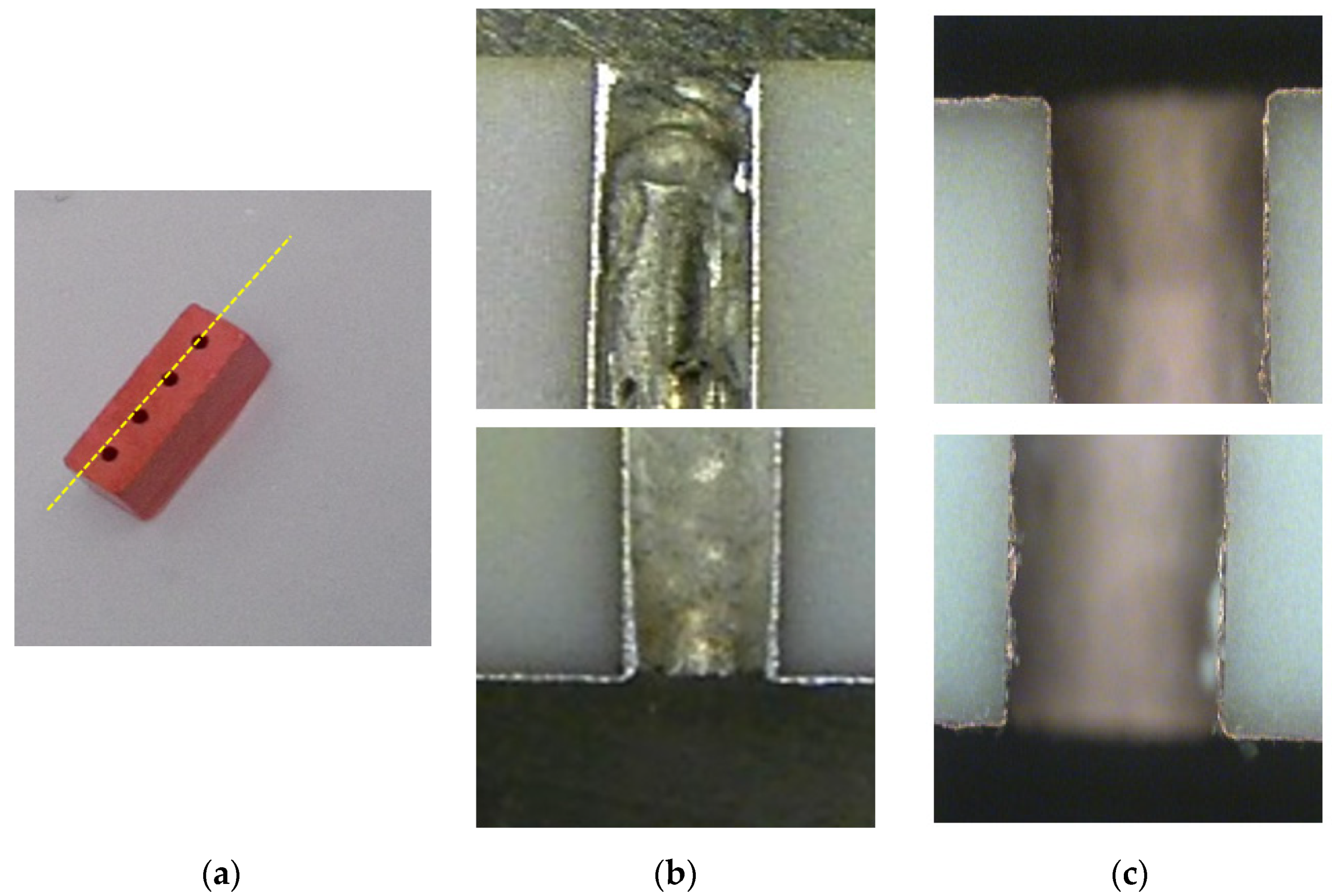
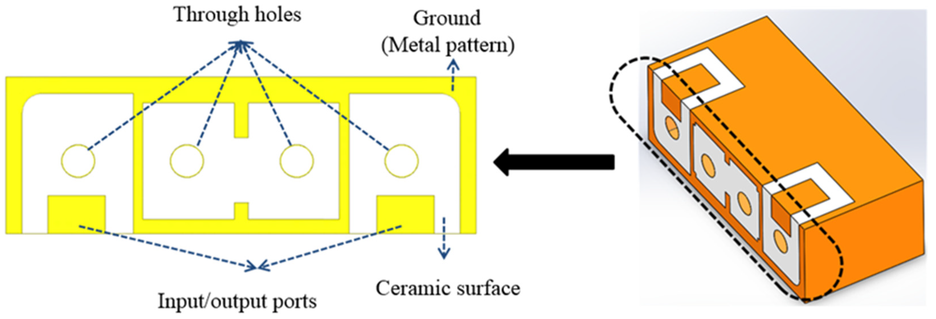
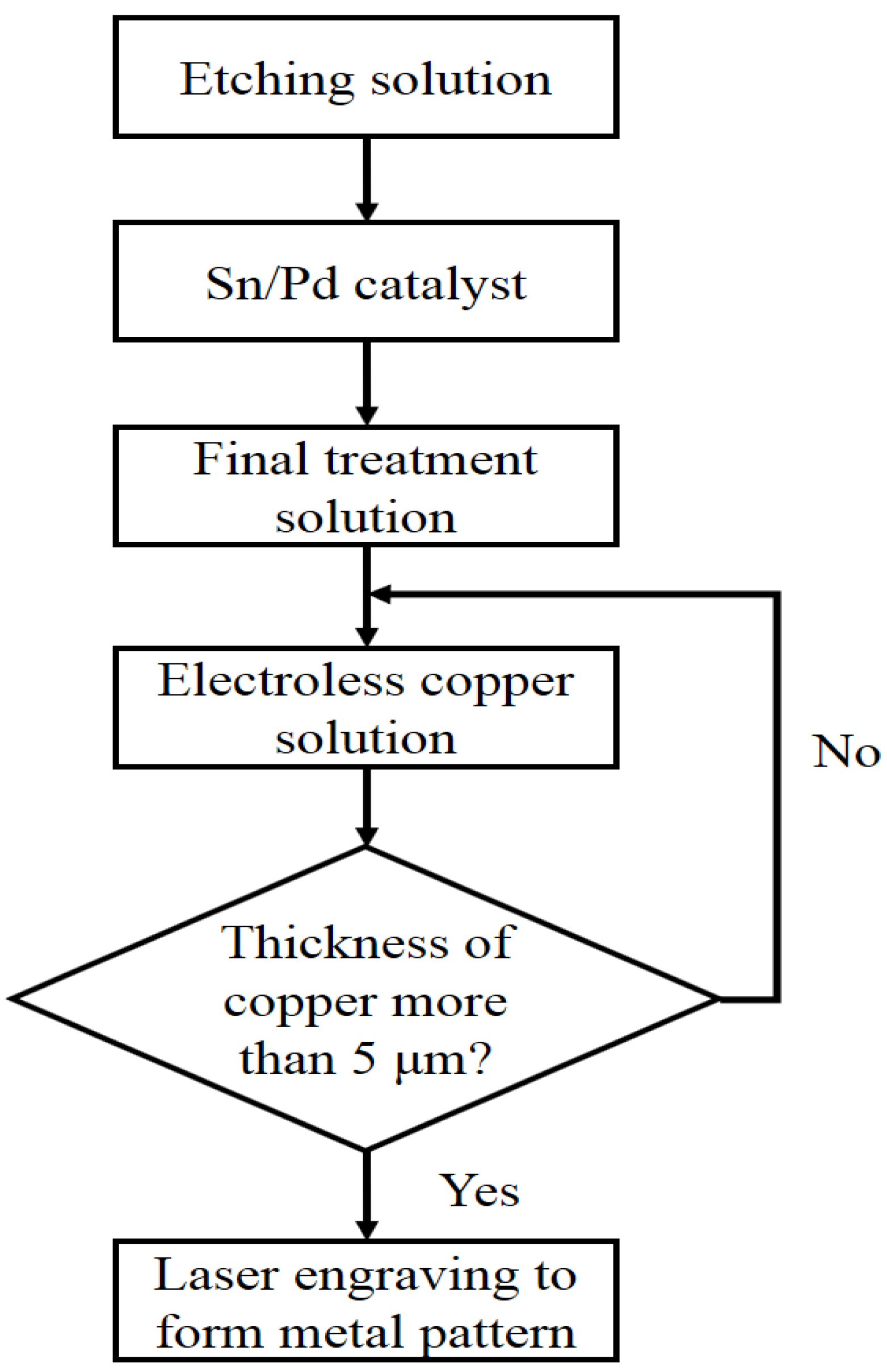
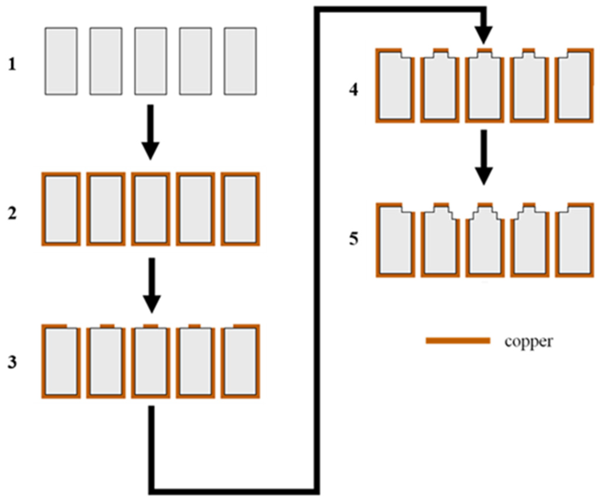
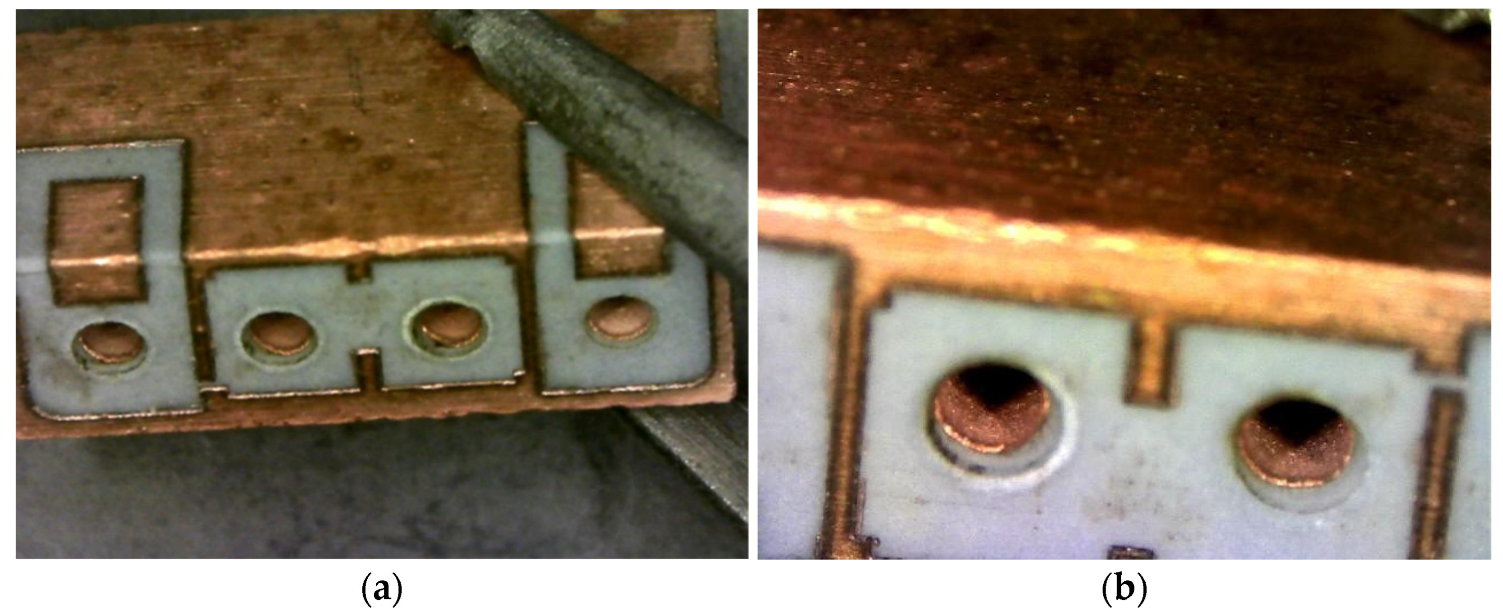
2. Low-Temperature Metallization Process and Filter Specification
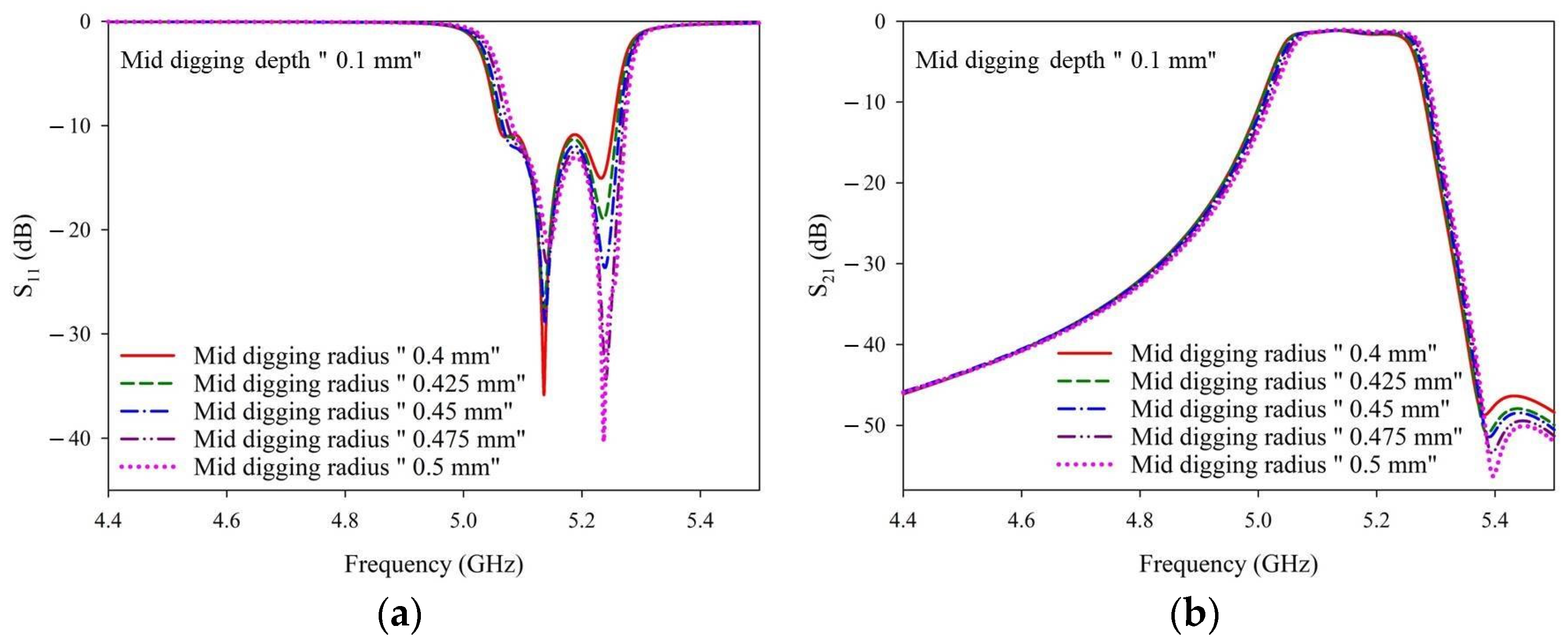
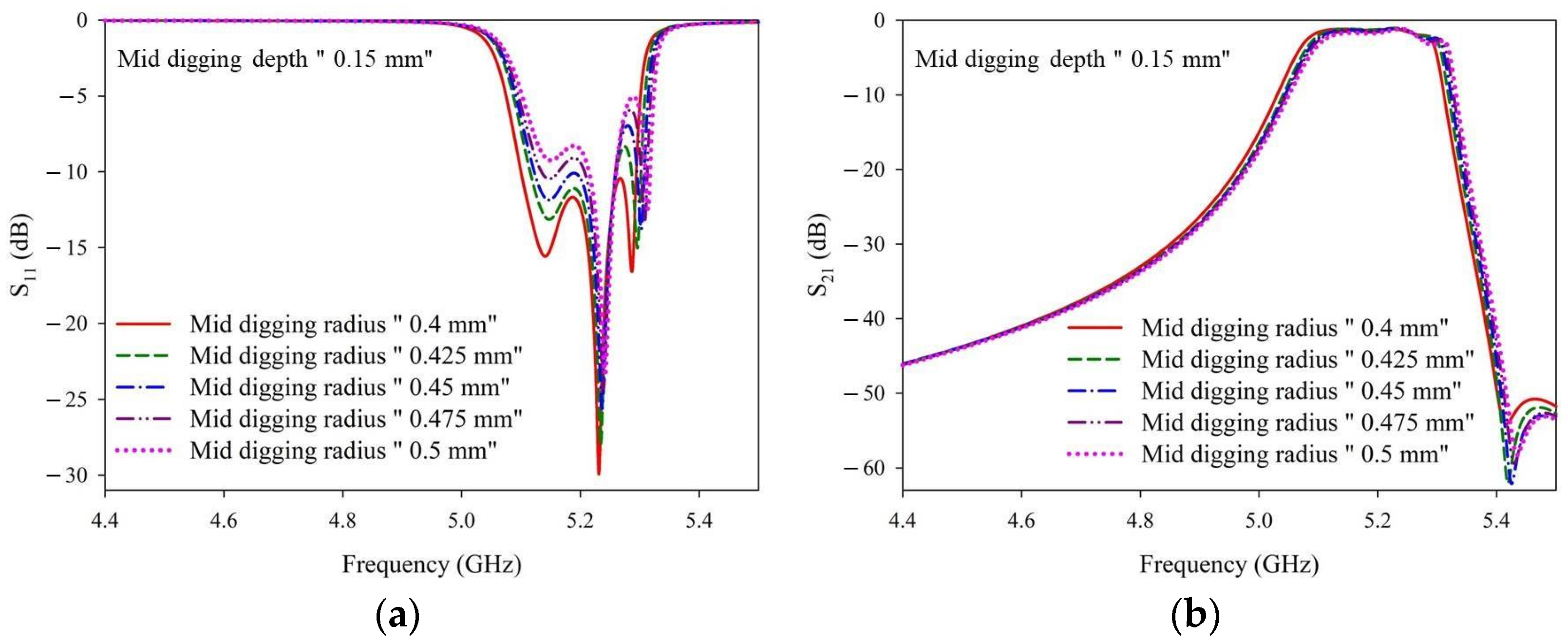
3. Electromagnetic Simulations
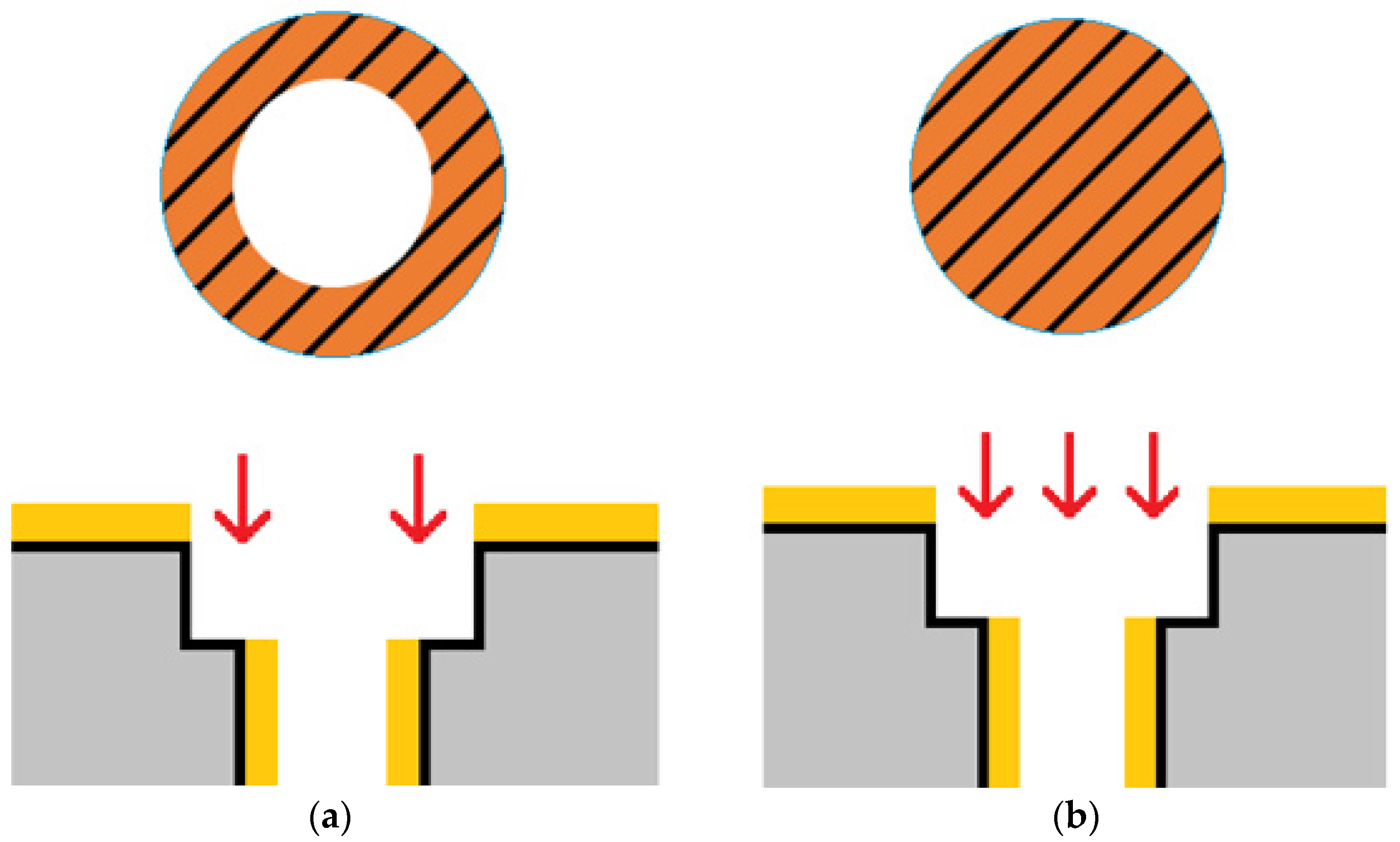
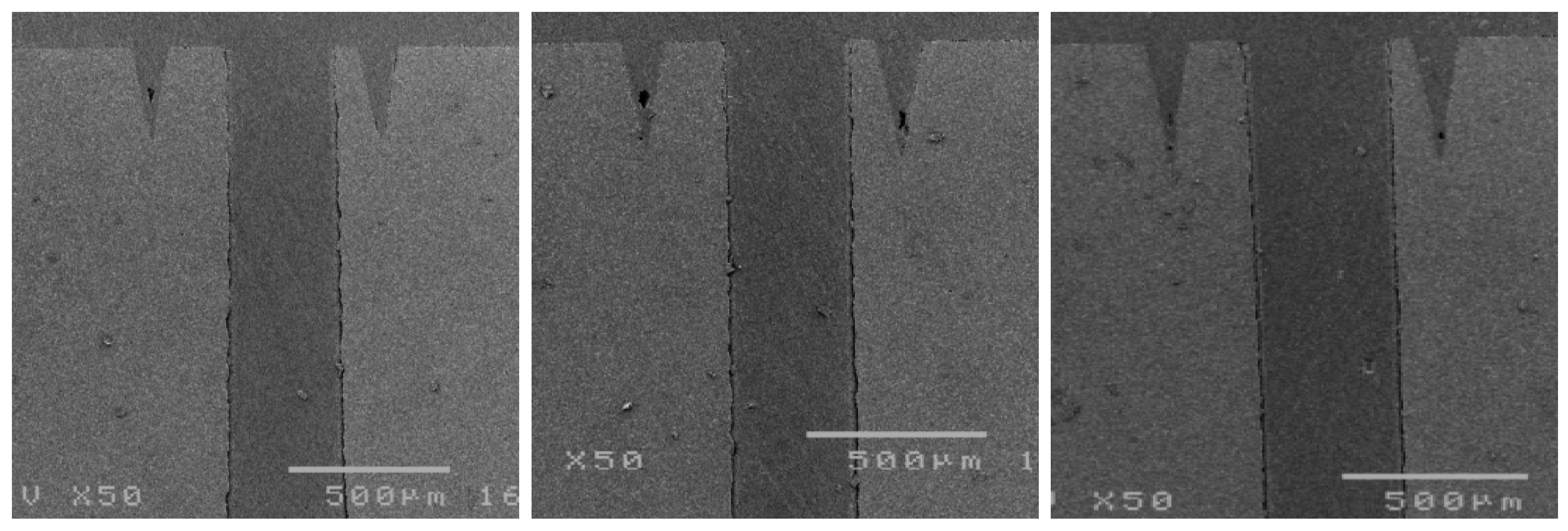
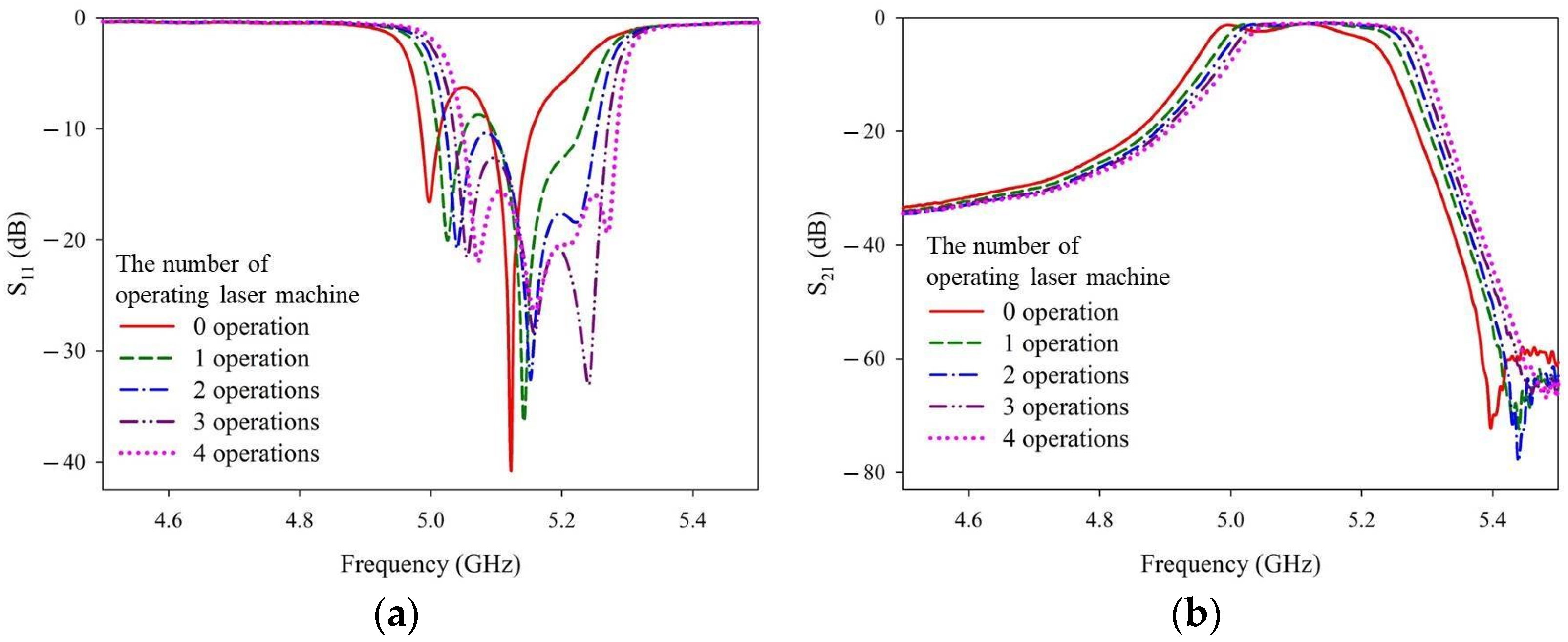
4. Laser Trimming Parameters, Operation Times, and Digging Depths
5. Final Manufacture Process and Measurement Results
6. Conclusions
Author Contributions
Funding
Institutional Review Board Statement
Informed Consent Statement
Data Availability Statement
Acknowledgments
Conflicts of Interest
Appendix A

| Digging Hole Depth (mm) | fL (GHz) | fH (GHz) | BW (MHz) | The Highest S11 Value in Passband (dB) | S21 < −3 dB in Passband? |
|---|---|---|---|---|---|
| 0 | 4.984 | 5.132 | 148 | −4.20 | 5.028–5.049 < −3 dB |
| 0.05 | 5.008 | 5.176 | 168 | −5.97 | Yes (Bad S11) |
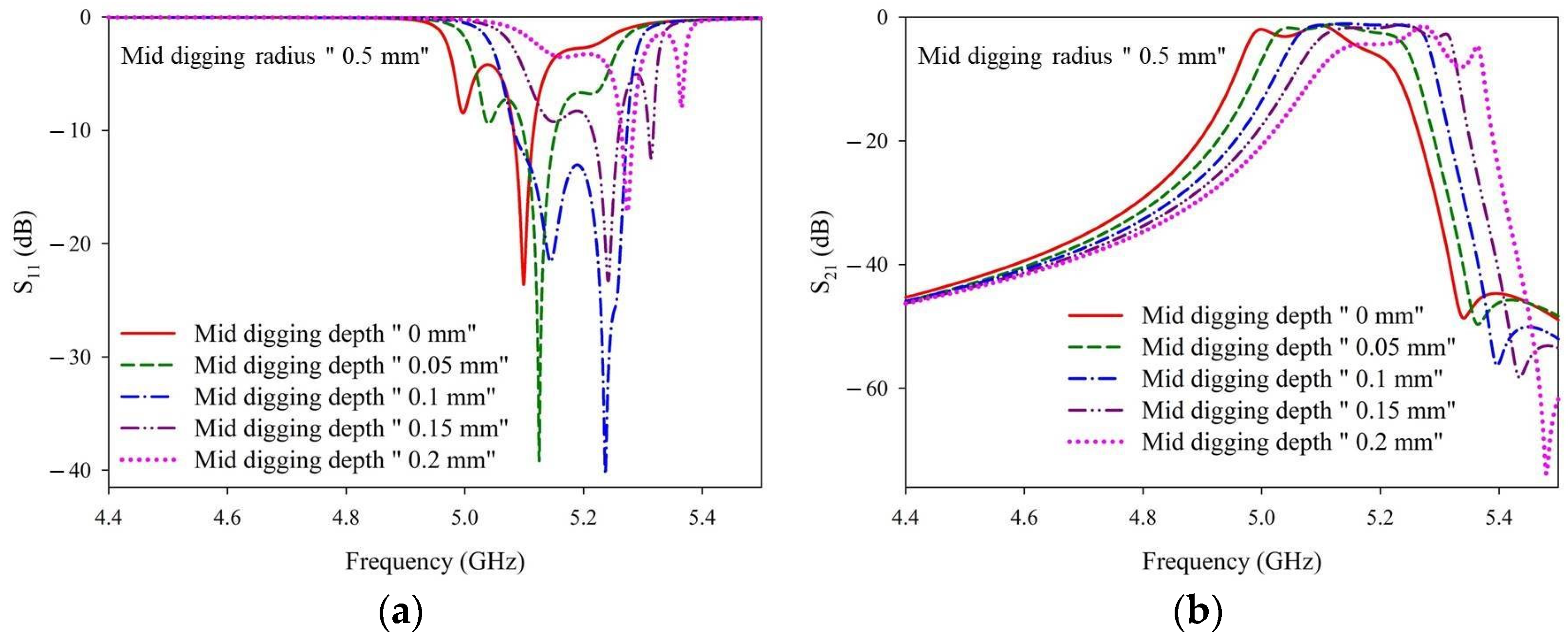
| 0.1 | 5.043 | 5.256 | 213 | −10.84 | Yes |
| 0.15 | 5.076 | 5.293 | 217 | −10.43 | Yes |
| 0.2 | 5.131 | 5.281 | 150 | −5.85 | Yes (Bad S11) |
| Digging Hole Depth (mm) | fL (GHz) | fH (GHz) | BW (MHz) | The Highest S11 Value in Passband (dB) | S21 < −3 dB in Passband? |
|---|---|---|---|---|---|
| 0 | 4.984 | 5.132 | 148 | −4.20 | 5.028–5.049 < −3 dB |
| 0.05 | 5.022 | 5.220 | 198 | −6.66 | Yes (Bad S11) |
| 0.1 | 5.061 | 5.274 | 213 | −13.05 | Yes |
| 0.15 | 5.104 | 5.315 | 211 | −5.05 | 5.280–5.303< −3 dB |
| 0.2 | 5.245 | 5.292 | 47 | ----- | Fail |
| Digging Hole Depth (mm) | fL (GHz) | fH (GHz) | BW (MHz) | The Highest S11 Value in Passband (dB) | S21 < −3 dB in Passband? |
|---|---|---|---|---|---|
| 0.4 | 5.043 | 5.256 | 213 | −10.84 | Yes |
| 0.425 | 5.045 | 5.260 | 215 | −11.30 | Yes |
| 0.45 | 5.050 | 5.265 | 215 | −11.94 | Yes |
| 0.475 | 5.056 | 5.270 | 214 | −12.50 | Yes |
| 0.5 | 5.061 | 5.274 | 213 | −13.05 | Yes |
| Digging Hole Depth (mm) | fL (GHz) | fH (GHz) | BW (MHz) | The Highest S11 Value in Passband (dB) | S21 < −3 dB in Passband? |
|---|---|---|---|---|---|
| 0.4 | 5.076 | 5.293 | 217 | −10.43 | Yes |
| 0.425 | 5.087 | 5.301 | 214 | −8.33 | Yes (Bad S11) |
| 0.45 | 5.093 | 5.306 | 213 | −6.95 | Yes (Bad S11) |
| 0.475 | 5.097 | 5.311 | 214 | −5.92 | Yes (Bad S11) |
| 0.5 | 5.104 | 5.315 | 211 | −5.05 | 5.280–5.303 < −3 dB |
References
- Liu, B.; Sha, K.; Zhou, M.F.; Song, K.X.; Huang, Y.H.; Hu, C.C. Novel low-εr MGa2O4 (M = Ca, Sr) microwave dielectric ceramics for 5 G antenna applications at the Sub-6 GHz band. J. Eur. Ceram. Soc. 2021, 41, 5170–5175. [Google Scholar] [CrossRef]
- Szwagierczak, D.; Synkiewicz-Musialska, B.; Kulawik, J.; Pałka, N. LTCC and Bulk Zn4B6O13–Zn2SiO4 Composites for Submillimeter Wave Applications. Materials 2021, 14, 1014. [Google Scholar] [CrossRef]
- Zhang, R.; Liu, J.; Wang, Y.; Luo, Z.; Zhang, B.; Duan, J. Flexible Wearable Composite Antennas for Global Wireless Communication Systems. Sensors 2021, 21, 6083. [Google Scholar] [CrossRef]
- Lee, B.D.; Yoon, K.H.; Kim, E.S.; Kim, T.H. Microwave dielectric properties of CaTiO3 and MgTiO3 thin films. Jpn. J. Appl. Phys. 2003, 42, 6158. [Google Scholar] [CrossRef]
- Huang, C.-L.; Weng, M.-H. Improved high Q value of MgTiO3-CaTiO3 microwave dielectric ceramics at low sintering temperature. Mater. Res. Bull. 2001, 36, 2741–2750. [Google Scholar] [CrossRef]
- Hao, S.; Shun-Hua, W.; Hai-yang, Y. Dielectric properties of B2O3 doped MgTiO3-CaTiO3 system ceramics. J. Wuhan Univ. Technol., Mater. Sci. Ed. 2004, 19, 62–64. [Google Scholar] [CrossRef]
- Jantunen, H.; Rautioaho, R.; Uusimäki, A.; Leppävuori, S. Compositions of MgTiO3–CaTiO3 ceramic with two borosilicate glasses for LTCC technology. J. Eur. Ceram. Soc. 2000, 20, 2331–2336. [Google Scholar] [CrossRef]
- Tummala, R.R. Ceramic and glass-ceramic packaging in the 1990s. J. Am. Ceram. Soc. 1991, 74, 895–908. [Google Scholar] [CrossRef]
- Sebastian, M.T.; Jantunen, H. Low loss dielectric materials for LTCC applications: A review. Int. Mater. Rev. 2008, 53, 57–90. [Google Scholar] [CrossRef]
- Narang, S.B.; Bahel, S. Low loss dielectric ceramics for microwave applications: A review. J. Ceram. Process. Res. 2010, 11, 316–321. [Google Scholar]
- Li, W.; Huang, M.; Kao, T.; Chung, W.; Chou, M. Novel LIM (Laser Induced Metallization) technologies of ITRI applied to WWAN/LTE 2-port antenna array for smart handset applications. In IEEE Antennas and Propagation Magazine, Proceedings of the 2014 International Symposium on Antennas and Propagation Conference Proceedings, Kaohsiung, Taiwan, 2–5 December 2014; Institute of Electrical and Electronics Engineers: Piscataway, NJ, USA, 2014; pp. 599–600. [Google Scholar]
- Yang, C.; Chou, M.; Kao, T.; Huang, M. Applications of Three Dimensional Laser Induced Metallization Technology with Polymer Coating. In Proceedings of the 2018 13th International Congress Molded Interconnect Devices (MID), Würzburg, Germany, 25–26 September 2018; pp. 1–6. [Google Scholar]
- Lin, J.-J.; Lin, C.-I.; Kao, T.-H.; Huang, M.-C. A Novel Low Temperature Process for Microwave Dielectric Ceramics Metallization. Appl. Comput. Electromagn. Soc. J. 2019, 34, 1601–1606. [Google Scholar]
- Rawat, B.S.; Beilke, L.; Miller, R.E. Design of a tapered coaxial resonator filter for mobile communications. IEEE Trans. Veh. Technol. 1992, 41, 1–5. [Google Scholar] [CrossRef]
- Maas, S. Coaxial Resonator Filters. Master’s Thesis, Stellenbosch University, Stellenbosch, South Africa, 2011. [Google Scholar]


| Material | Dk | Q × f (GHz) | Sintering Temperature (°C) | TCK (ppm/°C) |
|---|---|---|---|---|
| MgTiO3 [4] | 17 | 16,000 @ 7 GHz | 800 | −50 |
| CaTiO3 [4] | 170 | 3600 @ 7 GHz | 800 | 800 |
| 0.95 MgTiO3-0.05 CaTiO3 + 2 wt%B2O3 [5] | 21.2 | 62,000 @ 8 GHz | 1400 | 4 |
| 0.95 MgTiO3-0.05 CaTiO3 + 3.5 wt%B2O3 [6] | 20.3 | 68,000 @ 6 GHz | 1210 | −5 |
| MgTiO3-CaTiO3 [7] | 18–20 | 4000 @ 6 GHz | 1360 | −10 to 10 |
| Passband | Input and Output Matching (S11 and S22) | In-Band Loss (S21 and S12) | Image Rejection at ~5.5 GHz | ||
|---|---|---|---|---|---|
| fL (GHz) | fH (GHz) | BW (MHz) | |||
| 5.15 | 5.33 | 180 | <−10 dB | >−3 dB | <−60 dB |
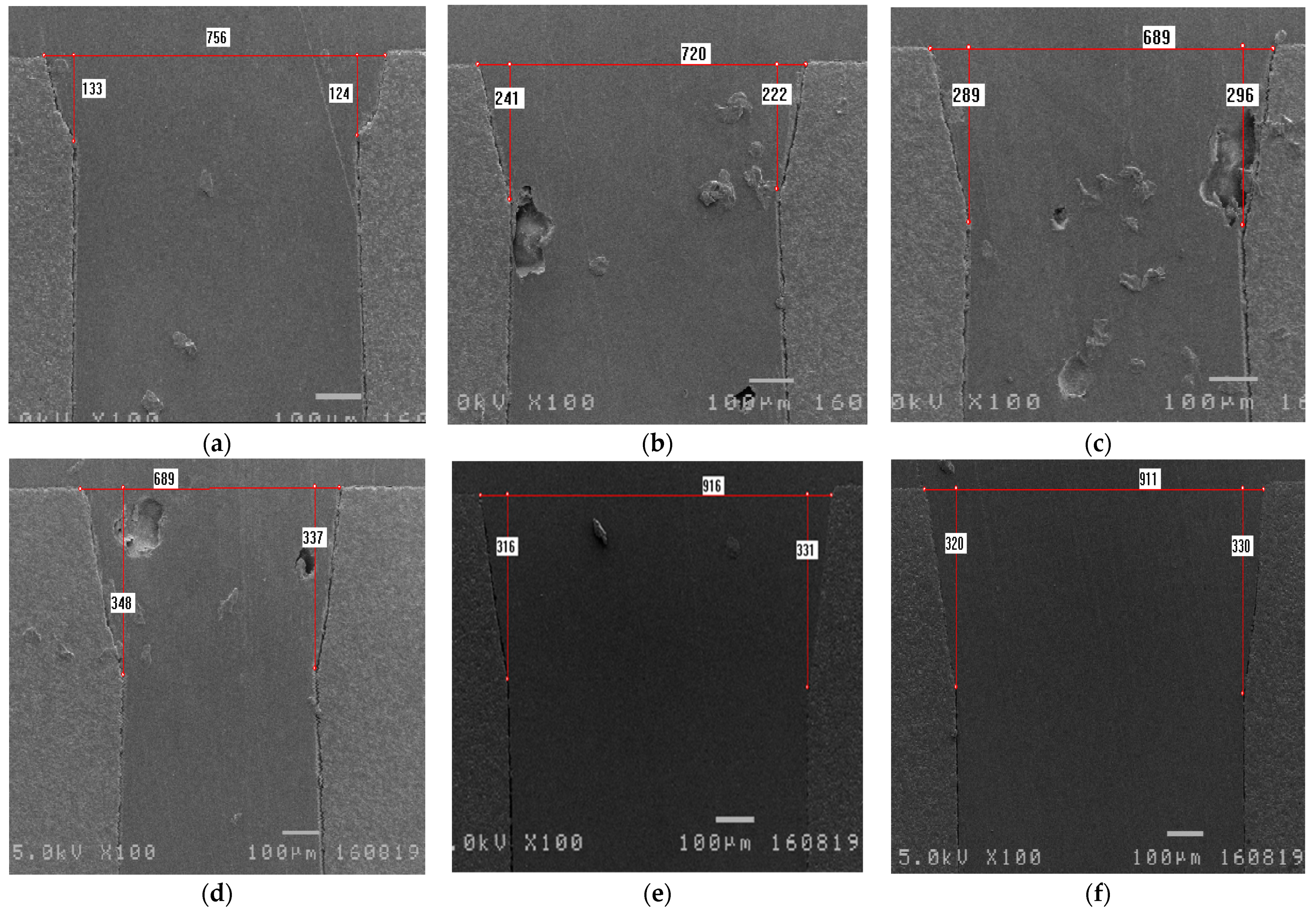
| Number of Repeated Laser Firings | Depth on the Left Edge (µm) | Depth on the Right Edge (µm) | Depth Difference (µm) | Depth Average (µm) |
|---|---|---|---|---|
| One | 133 | 124 | 9 | 143.5 |
| Two | 241 | 222 | 19 | 231.5 |
| Three | 289 | 296 | 7 | 292.5 |
| Four | 348 | 337 | 11 | 342.5 |
| Five | 316 | 331 | 15 | 338.5 |
| Six | 320 | 330 | 10 | 325 |
| Number of Repeated Laser Firings | Depth on the Left Edge (µm) | Depth on the Right Edge (µm) | Depth Difference (µm) | Depth Average (µm) |
|---|---|---|---|---|
| One | 170 | 174 | 4 | 172 |
| Two | 287 | 296 | 9 | 291.5 |
| Three | 276 | 315 | 39 | 295.5 |
| Four | 302 | 336 | 34 | 319 |
| Five | 291 | 343 | 52 | 317 |
| Six | 300 | 330 | 30 | 315 |
| Number of Repeated Laser Firings | Depth on the Left Edge (µm) | Depth on the Right Edge (µm) | Depth Difference (µm) | Depth Average (µm) |
|---|---|---|---|---|
| One | 15.90 | 22.97 | 7.07 | 19.44 |
| Two | 37.10 | 45.94 | 8.84 | 41.52 |
| Three | 70.67 | 77.76 | 7.09 | 74.22 |
| Four | 72.46 | 70.67 | 1.79 | 71.57 |
| Number of Repeated Laser Firings | Depth on the Left Edge (µm) | Depth on the Right Edge (µm) | Depth Difference (µm) | Depth Average (µm) |
|---|---|---|---|---|
| One | 24.73 | 30.09 | 5.36 | 27.41 |
| Two | 65.37 | 93.64 | 28.27 | 79.51 |
| Three | 132.51 | 123.69 | 8.82 | 128.10 |
| Four | 153.71 | 166.08 | 12.37 | 159.90 |
| Number of Repeated Laser Firings | Depth on the Left Edge (µm) | Depth on the Right Edge (µm) | Depth Difference (µm) | Depth Average (µm) |
|---|---|---|---|---|
| One | 65.39 | 61.84 | 3.55 | 63.62 |
| Two | 98.96 | 104.25 | 5.29 | 101.61 |
| Three | 120.14 | 134.28 | 14.14 | 127.21 |
| Four | 162.54 | 178.45 | 15.91 | 170.50 |
| fL (GHz) | fH (GHz) | BW (MHz) | Highest S11 Value in Passband (dB) | S21 > −3 dB in Passband? | Image Rejection < −60 dB at ~5.5 GHz | |
|---|---|---|---|---|---|---|
| Measured data (before) | 4.991 | 5.178 | 187 | −5.76 | Yes (Bad S11) | Yes |
| Measured data (after) | 5.15 | 5.33 | 180 | −11.77 | Yes | Yes |
| LTCC Process [7] | Proposed Process | |
|---|---|---|
| Temperature of metallization process (°C) | 900~1000 | <50 |
| Metal clogged in holes | Yes | No |
| Minimum metal line width (µm) | 100 | 50 |
| Relative position of lines (µm) | ±100 | ±50 |
| Mass production | Yes | Not yet |
Publisher’s Note: MDPI stays neutral with regard to jurisdictional claims in published maps and institutional affiliations. |
© 2021 by the authors. Licensee MDPI, Basel, Switzerland. This article is an open access article distributed under the terms and conditions of the Creative Commons Attribution (CC BY) license (https://creativecommons.org/licenses/by/4.0/).
Share and Cite
Lin, J.-J.; Lin, C.-I.; Kao, T.-H.; Huang, M.-C. Low-Temperature Metallization and Laser Trimming Process for Microwave Dielectric Ceramic Filters. Materials 2021, 14, 7519. https://doi.org/10.3390/ma14247519
Lin J-J, Lin C-I, Kao T-H, Huang M-C. Low-Temperature Metallization and Laser Trimming Process for Microwave Dielectric Ceramic Filters. Materials. 2021; 14(24):7519. https://doi.org/10.3390/ma14247519
Chicago/Turabian StyleLin, Jau-Jr, Cheng-I Lin, Tune-Hune Kao, and Meng-Chi Huang. 2021. "Low-Temperature Metallization and Laser Trimming Process for Microwave Dielectric Ceramic Filters" Materials 14, no. 24: 7519. https://doi.org/10.3390/ma14247519
APA StyleLin, J.-J., Lin, C.-I., Kao, T.-H., & Huang, M.-C. (2021). Low-Temperature Metallization and Laser Trimming Process for Microwave Dielectric Ceramic Filters. Materials, 14(24), 7519. https://doi.org/10.3390/ma14247519