1. Introduction
Since their discovery in 2009 [
1,
2,
3], perovskite solar cells (PSCs) have drawn great attention. Besides their low-cost solution processing, PSCs also possess favourable optoelectronic properties including a high absorption coefficient in the visible part of solar spectrum [
4], low recombination rate [
5], high mobility of charge carriers [
6] and a tuneable bandgap [
7]. In the past decade, their power conversion efficiency (
PCE) has been significantly enhanced from 3.8% in 2009 [
1] to more than 25% in single-junction architectures and more than 29% in silicon-based tandem cells [
8,
9,
10]. The enhancement of the
PCE, one of the key factors of solar cells, defines PSCs as the promising candidates for commercialization in the solar cell industry. Furthermore, many efforts have been made to develop advanced structures of perovskites [
11] for applications in photolysis, photodetectors [
12] and various type of solar cells such as flexible cells [
13], carbon-electrode-based cells [
14], semi-transparent cells [
15], tandem cells [
16], integrated cells [
17], switchable cells [
18], and single crystal cells [
19]. Perovskite solar cells are photovoltaics with solution processed active layer, one of several recently studied technology. The other broadly investigated photovoltaics with solution processed active layer, include photovoltaics based on the organic semiconductors as active layers [
20,
21,
22]. All of these PSC devices are supposed to have high power efficiency, high stability, and large-scale applicability. However, there are still several issues in practical operations of PSCs, such as the long-term instability due to the perovskite degradation (moisture, UV light, overheating) [
11,
23,
24], the toxicity of the most commonly used compounds [
25], and the current-voltage hysteresis in devices [
26]. In order to solve these obstacles, many methods have been used, such as doping ions in perovskite materials, charge transporting layer modification, modification of microstructure, and utilizing advanced fabrication techniques [
11].
The mostly used perovskite materials are methylammonium lead triiodide (MAPbI
3) and formamidinium lead triiodide (FAPbI
3), and their use as the absorber layer in PSCs has been extensively studied [
27,
28]. The results have shown that FAPbI
3 is thermally more stable, which makes it the most promising perovskite material for single-junction PSCs. Recently, rubidium and cesium cation (Rb
+ and Cs
+) incorporation emerged as a strategy to enhance PSCs efficiency [
29].
In conjunction with the perovskite materials as the photoactive absorber layer, other thin film materials are used to extract photogenerated electrons and holes, reducing charge recombination inside the absorber layer and improving the overall efficiency of the solar cell. Indeed, such layers have their energy band levels aligned in a way which creates a potential difference that drives the charge separation. For the charge separation of electrons, the material has to have lower conduction band (CB) maximum and valence band (VB) minimum energy levels than those of the absorber layer in order to promote electron extraction and block hole extraction from the active layer. These materials are called electron transport layer (ETLs) and most commonly used are TiO
2, ZnO and SnO
2 [
30]. Analogous to ETLs, materials which have higher CB maximum and VB minimum energy levels in comparison to those levels of the absorber layer, promote hole extraction and block electron extraction. These layers are called hole transport layers (HTLs) and the most popular are spiro-OMeTAD, P3HT, PTTA and PEDOT:PPS organic semiconductors [
31].
Since the main aim of numerous experimental studies is increase of the device
PCE, it is worth theoretically studying the influence of the specific parameters on the performance of the PSC by applying an appropriate model. In this work, we have employed one dimensional theoretical model of solar cell integrated in the solar cell capacitance simulator (SCAPS-1D) [
32] in order to elucidate which experimental procedure could improve the PSC parameters. The parameters that we varied by SCAPS-1D simulation and that can be influenced experimentally are: (1) acceptor doping concentration (
NA) of the perovskite absorber layer, (2) defect density in the perovskite absorber layer, (3) the thickness of the perovskite absorption layer, (4) resistivity
Rs (the net effect of ohmic loss) and
Rshunt (the leakage current loss).
The first mentioned parameter, which can be influenced experimentally, is doping concentration
NA. There are several studies which attempted to investigate how to influence the charge carrier concentration during the synthesis of the perovskite thin films. Shi and co-workers [
33] investigated the influence of precursor concertation and solvent choice in a two-step deposition method of the absorber layer. They reported that the carrier density and the depletion field decrease with the increase of the concentration of CH
3NH
3PbI
3 immersion solution (CH
3NH
3I dissolved in isopropanol), and also showed that the inclusion of a polar solvent improved the charge collection by influencing the reaction kinetics for the formation of the perovskite films. Bi et al. [
34] investigated the role of the length of thermal annealing and show that the extended annealing time improved the crystallinity and grain size of the perovskite crystals, but also led to the reduction of hole concentration. While improved crystallinity led to better
FF and
Jsc values, ultraviolet photoelectron spectroscopy studies confirmed the reduction of the work function with increased the annealing time. Several authors also reported the effects of adding the cations or the anions in the perovskite active layer and its impact on carrier concentrations. Liu and co-workers [
35] introduced rubidium cations into the perovskite film. While the crystal structure remained the same, the quality of the film worsened, reducing the efficiency of the device. However, rubidium cations made the majority carrier type of the perovskite layer into p-type, and previously formed pn junction between the active layer and the spiro-MeOTAD layer was replaced with a new pn junction between the active layer and TiO
2. The influence of the anion composition was investigated by Kiermasch et al. [
36], who doped the MAPbI
3 perovskite with bromine anions and concluded that bromine’s addition did not influence the carrier concentration, but instead increased carrier lifetime. They hypothesize that the origin of the enhancement lies in the increase in shallow traps close to the conduction or valence band. These states partially trap charge carriers which can then be released back into the band before they recombine, leading to the increase of the
Voc while
Jsc and
FF both decreased.
Second parameter, density of defects, are mainly influenced by the nature of the crystallization of the perovskite thin film. The origin of the defects resides on the grain boundaries of the polycrystalline films as well as dangling bonds, uncoordinated atoms and surface dislocation on the film surface. Influencing the crystallization process, the amount of defect densities that occur in perovskite thin films can be altered. Tan et al. [
37] employed an additional post annealing treatment of the methylammonium chloride perovskite films. Those films changed their microstructural orientation from the randomly oriented to the preferred (110) crystal plane growth, made possible by exploiting the chlorine intermediate phase analogous to the mineral bridge phenomenon in the oriented attachment mechanism.
FF,
Jsc and
Voc were improved as a result of lowered trap state densities with regards to oriented crystal growth [
38]; indeed, another way to impact the crystallization mechanism is through additive engineering. Yang and associates [
39] used the ammonium benzenesulfonate as an active layer additive; its zwitterionic structure passivated both cationic and anionic defects at the grain boundaries, which influenced both the carrier lifetime and the power efficiency of the formed solar cells. Alongside zwitterion molecules, polymers can be also used for the defect passivation. Kojić et al. [
40] investigated the influence of polyvinylpyrrolidone as an additive and reported an increase in radiative recombination with smaller Urbach energy values as a consequence of carbonyl interactions with the Pb
2+ dangling bonds. Inorganic cations can also improve the amount of the trap states, and Ng et al. [
41] confirmed this with the inclusion of germanium cations in a quasi 2D/3D perovskite. The thermally stimulated currents with the addition of Ge
2+ impacted the trap states close to the valence or conduction bands, so perovskite had fewer available states for the electrons to occupy.
A third simulated parameter, the influence of the absorber layer thickness on the cell performance, is studied experimentally by several authors. Rai et al. [
42] developed an array of perovskite solar cell devices by varying the active layer thickness with the precursor concentration. In their results, the solar cell efficiency increased with the increase of the perovskite thickness primarily as a result of higher
Jsc values. This is attributed to the reduction of non-radiative decay channels with the increased thickness, and they conclude that thinner absorber layers lead to insufficient photo-generation and increased SRH recombination. Xiao et al. [
43] also varied the perovskite thickness with the precursor concentration, reporting maximum
Jsc values for the perovskite thickness of 630 nm. Moreover, they explained that increasing the thickness results in higher current densities as a result of the higher absorption, supported by the external quantum efficiency measurements in the 550–800 nm region. However, increasing the thickness increases the amount of the grain boundaries inside the film, creating charge recombination traps. The authors showed that, by employing a solvent annealing step after the perovskite crystal annealing, it was possible to control the grain size of the film, synthesizing micron thick films with high device efficiency by reducing the amount of grain boundaries.
Furthermore, we investigated the influence of two types of resistance that limit solar cell performance: the net effect of ohmic loss,
Rs, and the leakage current loss,
Rshunt. Low
Rs and high
Rshunt are preferred in order to have highly efficient solar cells. The most common contributors to series resistance,
Rs, are metal-semiconductor contacts of the solar cells. As the perovskite/hole transport layer/metal contacts are most prone to synthesis variability, influencing their chemical nature and interface can vastly reduce series resistance. The mostly used hole transport layer is the organic material spiro-MeOTAD. Ways to improve the performance of its conductive nature via additives such as tris(2-(1Hpyrazol-1-yl)-4-tert-butylpyridine)cobalt(III) tri[bis-(trifluoromethane)sulfonimide], bis-(trifluoromethane)sulfonimide lithium salt and/or 4-tertbutylpyridine are well established [
44]. Rong et al. [
45] report the addition of ditetrabutylammonium dichromate in the spiro-MeOTAD hole transport layer by using the four-probe measurements, and found an optimal amount of dichromate addition, which can influence pinhole formation, demonstrates better hole extraction properties and a smaller series resistance compared to the control devices. Guarnera et al. [
46] investigated the role of an inorganic Al
2O
3 buffer layer between the active layer and the spiro- MeOTAD hole transport layer. In their investigation, they have found that the
Voc and the
Jsc are similar between the control cells and the buffer layer cells. The most pronounced impact is shown in the
FF values, with an increase of 25% for cells with the buffer layer. The Al
2O
3 buffer layer not only inhibited the formation of a direct contact between the perovskite and the metal contact but showed no degradation during the first 350 h under the full solar illumination. In their investigation of carbon contacts for perovskite solar cells, Babu and co-workers [
47] have reported that the use of a thin chromium interlayer between the hole transport layer and the metal (carbon) contact with the thickness of 5 nm provided high shunt resistance and no significant series resistance due to its high ductility. Mundhass et al. [
48] have studied the series resistance of the perovskite solar cells using
Jsc-
Voc measurements; in their report, they found that for multi-cation perovskites, the direction of the current sweep (e.g., positive–negative) can impact the value of the series resistance, whereas the series resistance for mono-cation perovskites are independent on the direction of the current sweep. This gives information on how the composition of the perovskite layer can influence the values of the series resistance. In the same paper, they investigated the impact of PTAA hole transport layer thickness on the series resistance and found that the increase of the PTAA thickness reduces the values of
FF, requiring optimal synthetic approach for a film thin enough to have an optimal
FF but thick enough not to have pinholes, which can contribute towards shunt resistance. Conversely, there are approaches to film surface interactions by forming interlayers; Veeramutuhu and co-workers [
49] used polyvinylpyrrolidone as an interlayer between the perovskite and the hole transport layer, which led to the increase in carrier lifetime with significant reduction of the surface roughness of the perovskite. Hemasiri et al. [
50] reported similar results with the utilization of a MoS
2 interlayer between the perovskite and the hole transport layer; the MoS
2 interlayer was shown to facilitate the extraction of the photogenerated carriers, mitigating interfacial charge recombination.
A major contribution to low
Rshunt are the formation of pinholes and film porosity, and thus several experimental approaches to increase its value are reported in the literature. Brecker and Wark [
51] studied the impact of the solvent on the sequential deposition of the perovskite layer. By taking into account solvent permittivity, they have introduced pentan-1-ol into the MAI/isopropanol mixture, which eliminated the pinhole formations in the film and increased the power conversion efficiency by 60%. The usage of a compact TiO
2 blocking layer below the mesoporous TiO
2 film has found wide usage in the preparation of the perovskite solar cells, as it provides a way of eliminating shunt resistance issues in combination with the mesoporous TiO
2. Singh et al. [
52] investigated how the thickness of the compact layer impacts the performance of the solar cells; they report an optimal thickness of ~57 nm in order to reduce shunt losses as well as trap-assisted recombination and bimolecular recombination, which become more pronounced with increased compact layer thickness. Hörantner et al. [
53] have shown that long alkyl chained silane molecules can be used to block shunt pathways without obstructing the charge transfer of the solar cell devices, leading to the significant increase in the
Voc values, while other inorganic materials can also be used as passivation materials. Saranin et al. [
54] report the use of copper (I) iodide, which has been usually applied as a hole transport layer, as an interlayer between the perovskite and the electron transport layer in their experiments; the inclusion of CuI increased the efficiency of the solar cell as well as their shelf-life stability.
In this work, our intention was to simulate an average perovskite solar cell and use simulation to point out which parameters could be influenced to increase the power conversion efficiency of the device. As a starting point we have synthesized the mixed cation lead triiodide perovskite containing formamidinium, Rb+ and Cs+ ions (Rb0.05Cs0.1FA0.85PbI3) and applied it as an absorber layer in PSC devices with the architecture ITO/TiO2/perovskite/spiro-MeOTAD/Au. The obtained PCE was around 7%. In order to find routes to increase the PCE of the device, we have attempted to simulate the perovskite solar cell by using solar cell capacitance simulator (SCAPS) under standard AM1.5G illumination as a way to understand which parameters can affect its performance and what is the highest PCE is that we can theoretically achieve. We used a simulation model to optimize the following parameters influencing the PSC performance: acceptor doping concentrations, defect density, perovskite layer thickness, and resistances: series Rs (net effect of ohmic loss) and parallel Rshunt (the leakage current loss). Moreover, the influence of the interface between layers on PSC performance was discussed in detail.
The main insight of the simulation, showing new input for further optimization of the solar cell efficiency, was finding that the strongest impact on the device performance comes through resistivity of the layers. The negative impact of the resistivity on PSC performances could be improved by influencing layers’ structure quality. Therefore, lowering the density of the defects in layers and interlayers would lower the recombination rate in solar cells.
2. Materials and Methods
2.1. Materials Used for Preparation of Perovskite Solar Cells
For the synthesis of the Rb0.05Cs0.1FA0.85PbI3 perovskite, the following materials were used: lead (II) iodide (Sigma-Aldrich, 99%, St. Louis, MO, USA), formamidinium iodide (FAI) (Sigma-Aldrich, ≥99%, St. Louis, MO, USA), cesium iodide (Sigma-Aldrich, ≥99%, St. Louis, MO, USA), rubidium iodide (Sigma-Aldrich, ≥99%, St. Louis, MO, USA), N,N-dimethylformamide (DMF) (Merck, p.a., Darmstadt, Germany), dimethyl sulfoxide (DMSO) (Merck, p.a., Darmstadt, Germany), chlorobenzene (Merck, p.a., Darmstadt, Germany).
15 × 15 mm indium tin oxide (ITO) coated glass plates (Lumtech, ρ ~15 Ω/sq, CA, USA) were used as substrate and transparent front electrode. For the synthesis of the TiO2 ETL titanium diisopropoxide (Sigma-Aldrich, 99%, St. Louis, MO, USA), acetylacetonate (Sigma-Aldrich, 99%, St. Louis, MO, USA) and ethanol (Merck, p.a., Darmstadt, Germany) were used. For the preparation of the spiro-OMeTAD HTL, spiro-OMeTAD (Merck, ≥99%, Darmstadt, Germany), 4-tert-butylpyridine (tBP) (Sigma-Aldrich, 99%, St. Louis, MO, USA), FK209 (Sigma-Aldrich, 99%, St. Louis, MO, USA), bis-(trifluoromethane)sulfonimide lithium salt (LiTFSI) (Sigma-Aldrich, 99%, St. Louis, MO, USA) and acetonitrile (Merck, p.a., Darmstadt, Germany) were used.
2.2. Preparation and Characterization of Perovskite Solar Cells
In order to prepare the TiO2 ETL, 400 μL of acetylacetonate and 600 μL of titanium diisopropoxide were dissolved in 9 mL of ethanol. 50 μL of the prepared solution was spin coated on ITO glass substrates (4000 rpm, 2000 rpm/s) for 30 s and annealed at 450 °C for 2 h.
To prepare the perovskite thin films 461 mg of PbI2, 172 mg of FAI, 26 mg of CsI and 106 mg of RbI were dissolved in 1 mL of DMF/DMSO mixture (V(DMF):V(DMSO) = 4:1). Perovskite films were prepared inside a nitrogen-filled glovebox by spin coating 50 µL of the perovskite precursor on TiO2 substrates. The spin coating parameters were: 1000 rpm, 200 rpm/s for 10 s and 6000 rpm, 2000 rpm/s for 20 s. During the last 10 s, 50 µL of chlorobenzene was dripped onto the rotating substrate to improve the nucleation and crystal growth of the film. As prepared substrates were annealed on a hotplate at 150 °C for 10 min.
The spiro-OMeTAD was prepared by dissolving 50 mg of spiro-OMeTAD in 498 μL of chlorobenzene and adding 18 μL of tBP, 10 μL of LiTFSI stock solution and 4 μL of FK209 stock solution. The stock solutions of LiTFSI and FK209 were 1.8 mmol/mL and 0.25 mmol/mL in acetonitrile, respectively. Then 50 µL of the spiro-OMeTAD solution was spin coated on the perovskite/TiO2 substrate (4000 rpm, 1000 rpm/s) for 10 s. Before the gold depositions, the substrates were left resting overnight in dark and dry air. The final step included the deposition of 100 nm of gold contacts on the substrates.
Scanning electron microscopy image of prepared PSC was recorded using field emission scanning electron microscope (FE-SEM) model JSM-7000F manufactured by JEOL Ltd., Tokyo, Japan, using an accelerating voltage of 10 kV, equipped with an energy-dispersive X-ray spectrometer (EDS), EDS/INCA 350 (energy-dispersive X-ray analyser) manufactured by Oxford Instruments Ltd., Abingdon, UK.
The current density–voltage (J–V) curves of the solar cells were performed using a Keithley 2400 source meter and a LabView-based software inside a glove box (nitrogen atmosphere). For the J–V curves, the scan rates were adjusted to 100 mVs−1. The illumination area was defined using a shadow mask (0.07 cm2) and the light was provided by a Dedolight DLH500 lamp calibrated to an intensity of 100 mWcm−2 using a reference silicon solar cell (Fraunhofer ISE). The external quantum efficiency (EQE) spectrum was measured using a MuLTImode 4 monochromator (Amko) equipped with a 75 W xenon lamp and a Keithley 2400 source meter. The monochromatic light was chopped at a frequency of 30 Hz and the measurement setup was spectrally calibrated with a silicon photodiode (Newport Corporation, Irvine, CA, USA, 818-UV/DB). UV–Vis measurements of the perovskite absorber layer were performed using the UV/VIS Spectrometer—Lambda 35 by Perkin Elmer.
2.3. Numerical Simulation
Simulation of the solar cell was obtained by using SCAPS-1D software (solar cell capacitance simulator one dimension) which numerically solves one dimensional Poisson and continuity equations that govern the semiconductor material under the steady-state conditions [
32]. Poisson equation presents the relationship between the electric field of a p-n junction (
E) and the space charge density (
ρ) and is given by:
where
ψ is the electrostatic potential,
q is the elementary charge,
εs is the static relative permittivity of the medium,
n,
p are the electron and hole densities,
are the densities of ionized donors and acceptors and
Nt is possible defect (acceptor or donor) density [
55]. The electron and hole continuity equations in steady-state are given by:
where
jn,
jp are the electron and hole current densities,
G is the electron-hole pair generation rate, and
Rn,
Rp are the net recombination rates of electrons and holes. The electron and hole current densities are given by:
where
q is the elementary charge,
µn,
µp are the electron and hole mobility and
Dn,
Dp are the diffusion coefficients of the electrons and holes. SCAPS-1D software can simulate solar cell structures up to seven layers and extract their basic characteristics, such as the band diagram, the generation and recombination rates, the external quantum efficiency, the cell current densities, the
J–V characteristic with short-circuit current, open-circuit voltage, fill factor and power conversion efficiency. For SCAPS simulation, the input parameters are listed in
Table 1.
3. Results and Discussion
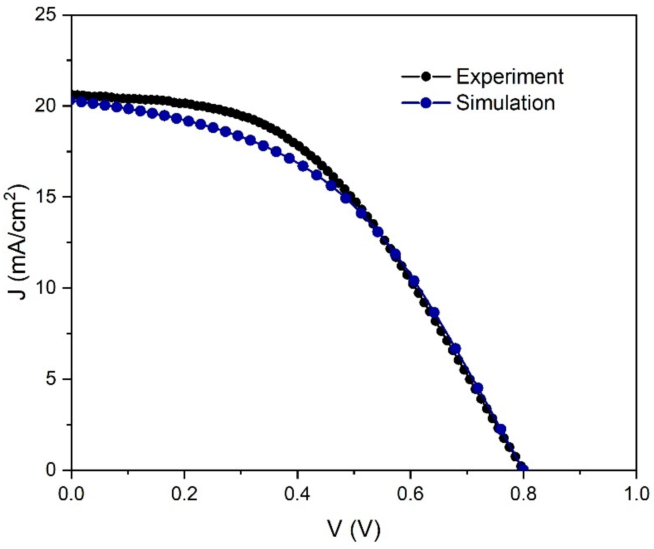
In the first step of our study, we have simulated the current density–voltage (
J–V) characteristic and cell performance parameters to obtain a good fit with the
J–V characteristic measured for our experimentally prepared PSC (
Figure 1).
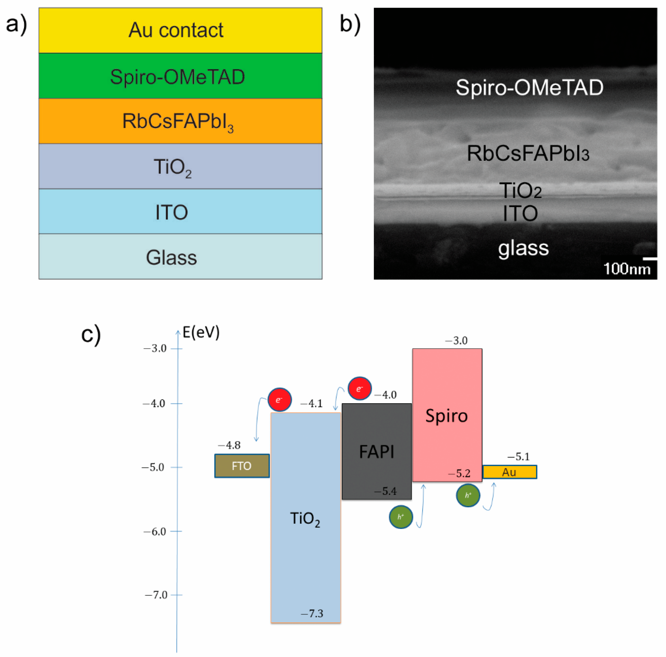
The layer structure of the prepared perovskite solar cell (Rb
0.05Cs
0.1FA
0.85PbI
3) is illustrated in
Figure 1a, its cross-sectional SEM image is shown in
Figure 1b, while the energy band diagram is shown in
Figure 1c. The energy band diagram (
Figure 1c) shows good matching of ETL and HTL with the absorption layer and allows a smooth flow of charge through the cell.
With the aim of increasing the PCE of our device, we have studied the influence of the specific parameters on performance of the PSC in order to elucidate which experimental procedure could improve the PSC parameters.
Experimental
J–V curve was obtained in a two-wire configuration with a Keithley 2400, under 100 mW/cm
2 illumination. Following, the simulation has been run with the input parameters of the structure summarized in
Table 1. They are based on previously published literature [
56,
57,
58,
59,
60,
61] and our experimental results.
Using above-mentioned initial parameters concerning the
J–V characteristic, simulation results gave the following solar cell performance parameters, which are listed and compared to experimentally obtained data in
Table 2.
Figure 2 shows a comparison between the simulation results and the experiment. A good match between measurements and simulation was observed for the current density/voltage characteristics validating our simulation.
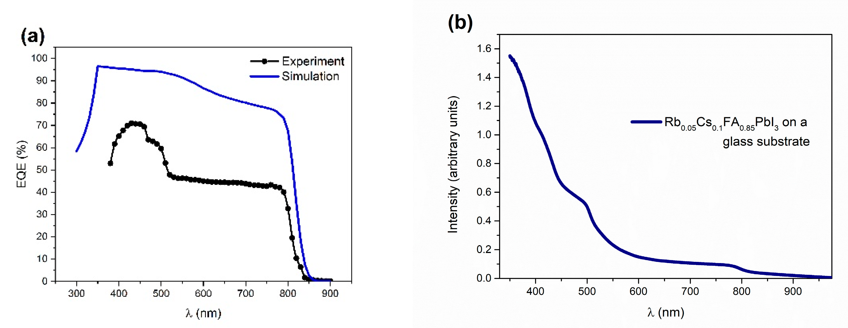
The external quantum efficiency (EQE) spectrum (experiment and simulation), along with the absorbance spectra of the perovskite film, are illustrated in
Figure 3. For the simulation of the EQE spectra, the absorption coefficient was calculated from the absorbance spectra. Both EQE curves show the optical absorption edge of the PSC that starts at 800 nm, with the disparity in the lower wavelength region (
Figure 3a). Higher experimental values of quantum efficiency on lower wavelength regions are in agreement with the rise in absorbance in the same region (
Figure 3b). However, as the mechanism of this experimentally observed behavior is unclear, except for a gradual increase in the EQE values, the simulated spectra could not completely fit the experimental data.
3.1. Doping Concentration Impact of Perovskite Active Layers on PSC Performance
In order to study how the concentration of
NA of the perovskite thin film impacts the performances of the solar cell, we have investigated
NA values in the range from 10
13 cm
−3 to 5·10
17 cm
−3 in the simulation. The rest of the parameters were fixed to values indicated in
Table 1.
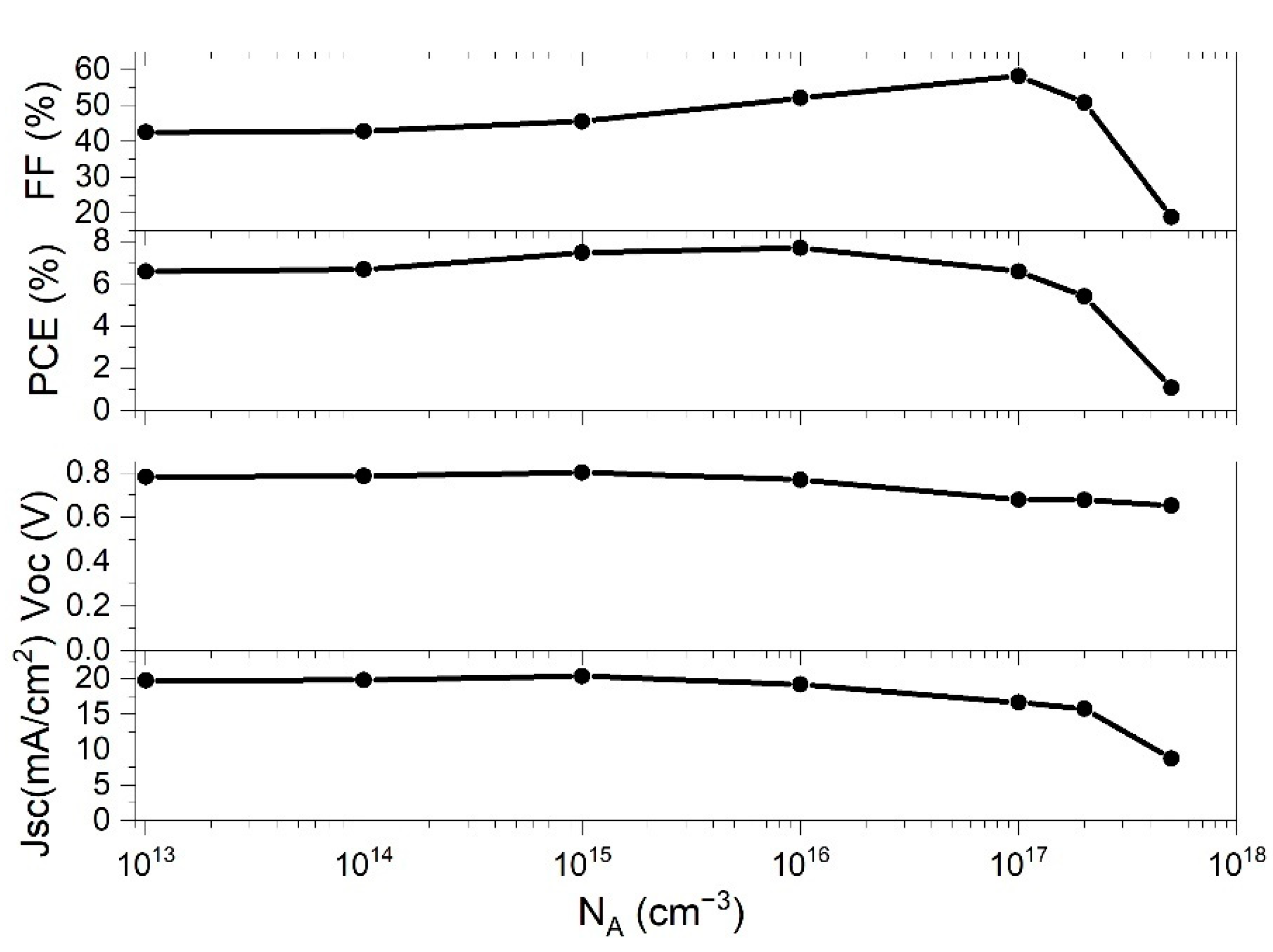
Figure 4 shows the behavior of the PSC parameters with the change of
NA.
The
FF slowly raised with the enhancement of
NA, and then rapidly decreased after
NA went beyond 10
17 cm
−3.
PCE exhibited similar behavior, having a maximum value at
NA = 10
16 cm
−3, and then rapidly decreased. The other two parameters,
Jsc and
Voc are also influenced by the change of
NA, both of which have their local maximum at ~10
15 cm
−3. At higher
NA concentrations,
Voc decreased slowly, while
Jsc decreased very rapidly after
NA exceeded 10
17 cm
−3. The difference of the cell performance in respect to the
NA can be explained by the rise of the built-in electric field with the increased concentration of the
NA [
16,
24]. Charge carriers separation is more pronounced with an increased electric field and consequently improves the performance of the cell. However, even larger values of
NA will lead to higher Auger recombination rates and subsequently PSC parameters will decrease [
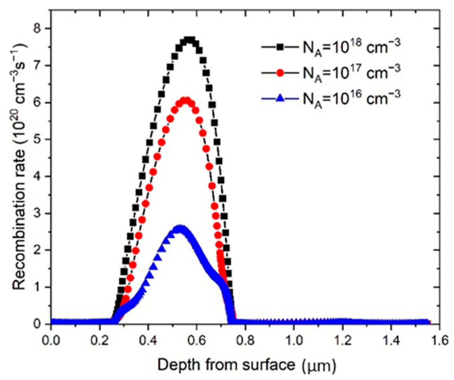
62]. As it can be seen in
Figure 5, the recombination rate,
R, is increased notably, starting with
NA values of 10
16 cm
−3, which is in good correlation with PSC parameters presented in
Figure 4.
Therefore, only a range of
NA values can contribute to the improvement of
Jsc and
Voc and the increase the
PCE value. The deposited perovskite films optimally have low charge carrier concentration in order to maximize the carrier mobility inside the perovskite thin film. At the
NA values of 10
16 cm
−3, the maximum
PCE of 7.71% was obtained, while the other parameters of PSC for that N
A concentration were
Voc = 0.77 V,
Jsc = 19.23 mA and
FF = 52.07% (see
Figure 4). The result of the simulation shows that our starting value for N
A, from the parameter set which optimally represents the experimental data (
Table 1), is very close to the optimal value obtained by theoretical modelling (
NA = 10
16 cm
−3).
Generally, doping concentration of the active layer in PSC could be optimized experimentally by changing synthesis precursor concentrations, solvent choice [
33], changing the length of thermal annealing [
34], or by adding the cations or the anions in the perovskite active layer [
35,
36], as was stated in detail in the introduction.
3.2. Defect Density Impact on PSC Performance
Regarding the improvement of the PSC performance, the defect density is an additional parameter that should be taken into account. The morphology and film quality of the perovskite have been shown to have an important influence on the performance of the perovskite solar cell [
63]. Poor quality and film coverage on mesoporous TiO
2 has shown to increase the charge recombination inside the active layer [
64], and the recombination is explained by the increase in the defect density (
Nt), which can impact the
Voc of the solar cell.
The Shockley–Read–Hall recombination model (SRH) was used to study the influence of the perovskite active layer defect density on the cell performance. The neutral defects were set at the center of the band gap following the Gaussian distribution with the characteristic energy value of 0.1 eV, and the characteristic energy of 0.1 eV were set to be at the center of the band gap. In the SRH recombination model, the recombination rate,
R, is defined as [
65,
66]:
where
n is the concentrations of the mobile electrons and
p is the concentrations of the holes. The concentrations of the charge carriers can be found by solving Poison and continuity equations; at positive voltage values, where
qV > 3
kT, the term
ni2, which explains the thermal generation, can be neglected.
Et is energy level, while
Nt is the concentration of the trap defects;
τn is the lifetime for the electrons, while
τp is the lifetime of the holes. They are given by equations:
where
σn is the capture cross-sections of the electrons,
σp is the captured cross-sections of the holes, while
vth is the thermal velocity.
The carrier diffusion length,
l, is is defined by the equation:
where
D is the diffusion coefficient with the equation:
where
μ is the charge carrier mobility. As Equation (7) indicates, when defect density decreases, the charge carrier lifetimes increase, leading to longer diffusion lengths (Equation (8)) and lower recombinations. These were the main factors influencing the improvement of the cell performance.
Defect density,
Nt, was investigated as a parameter in the PSC performance, and the defect density values were changed from 10
14 cm
−3 to 10
18 cm
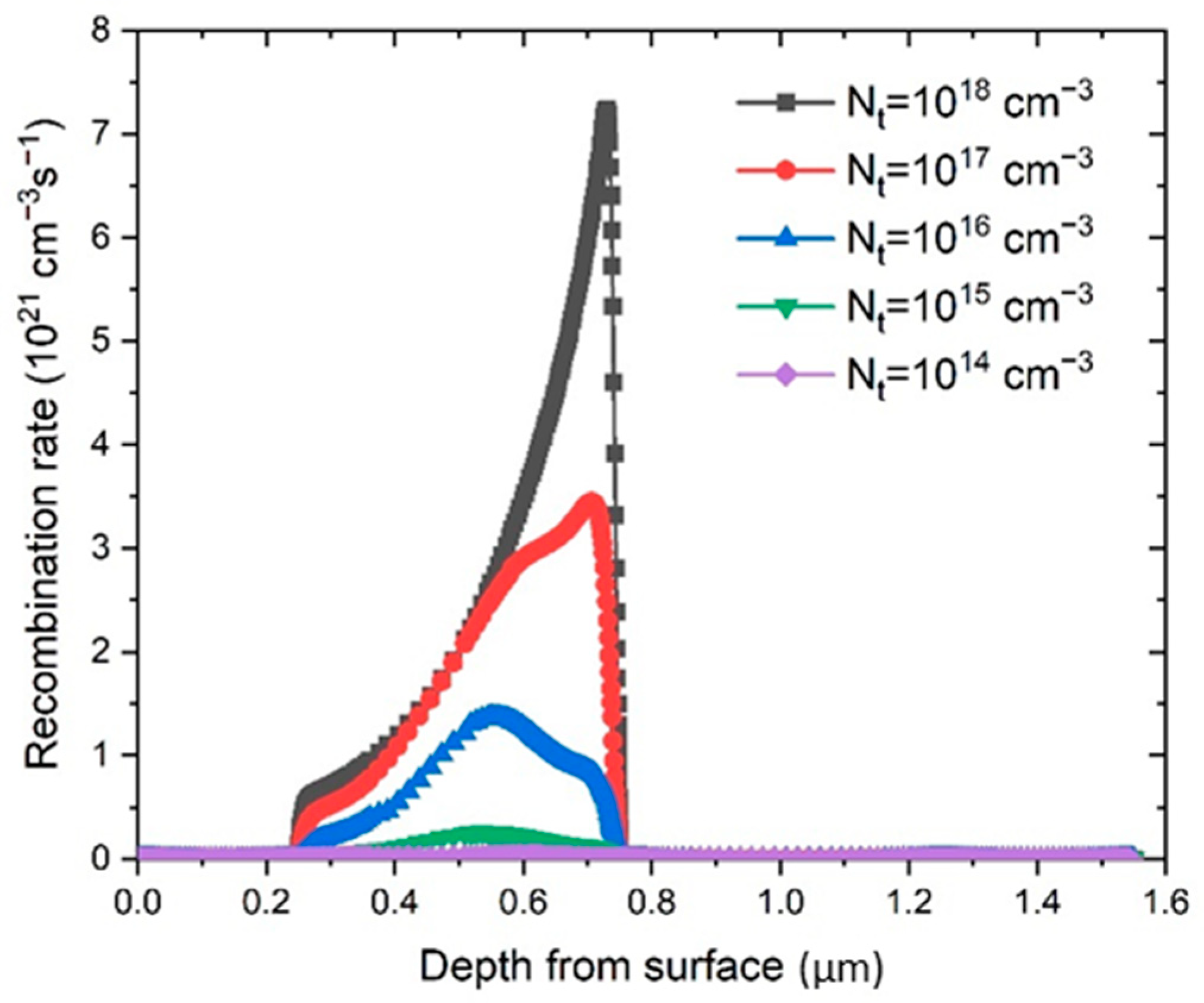
−3. The change in the recombination rate (
R) (Equation (6)) is shown in
Figure 6. It is clear that the reduction of
Nt lowers the recombination rate, and at the same time increases the diffusion length,
l.
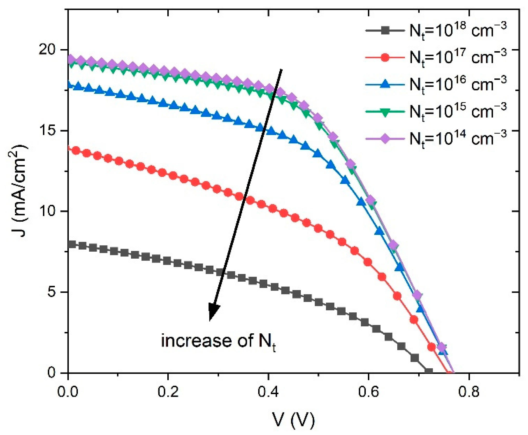
Therefore, the defect density reduction in the perovskite significantly improved the performance of the PSC, which is consistent with the simulation results showed in
Figure 7. The obtained simulated
J–V characteristics show an improvement of the PSC parameters with the reduction of
Nt.
The lowest defect density of 1·10
14 cm
−3 gives the best performance, but obtaining such a low
Nt in experiments is very difficult due to the polycrystalline nature of the perovskite films, and thus we set the optimized value of defect density at 1·10
15 cm
−3. As can be seen from
Table 1, that value was also the initial value of
Nt, which gave the best fit to the experimental voltage-V curve.
The defects can be interpreted as the faults inside experimentally obtained solar cells due to the grain boundaries or as dangling bonds, uncoordinated atoms, and surface dislocation on the film surface. As was presented in introduction, the defect density can be decreased experimentally by post annealing with the aim to obtain oriented crystal growth [
37,
38], with additive engineering [
39,
40], or by the inclusion of cations which impacted the trap states [
41].
3.3. Impact of the of the Perovskite Active Layer Thickness on the PCS Performance
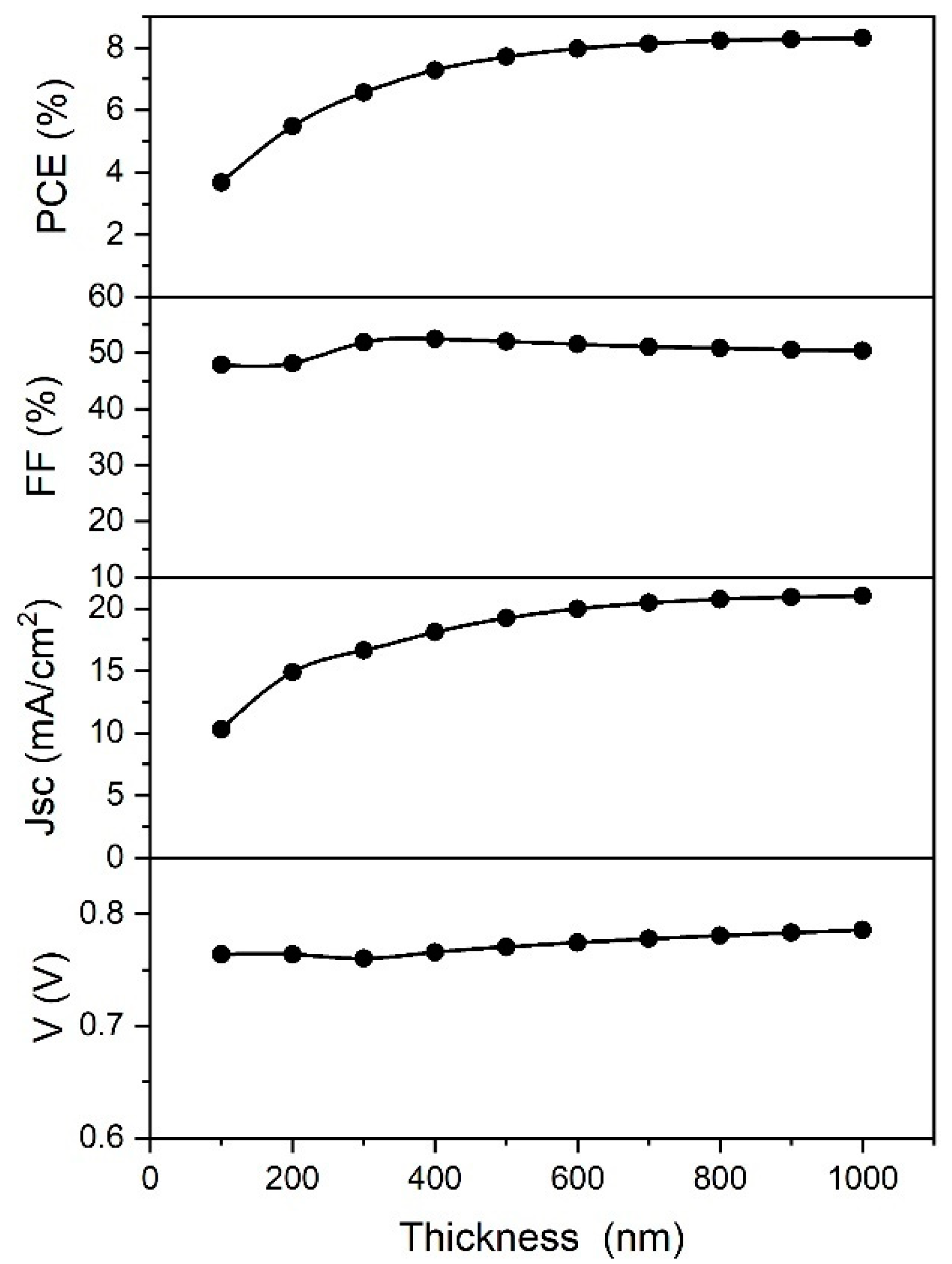
Absorbing layer thickness is another parameter that plays a very important role in the performance of thin film solar cells. The influence of the absorber layer thickness on the cell performance with is shown in
Figure 8.
When the thickness is too low, the absorption of the light is also very low, giving lower PCE values. As the thickness of the absorber is increased, the absorption of the light is increased as well, improving the PCE. With the thickness values larger than 800 nm, the PCE of the cell remains invariable. However, an increase in thickness leads to larger recombination rates in the bulk (depending on the diffusion length), saturating the PCE and Jsc values. This is the reason why the PCE shows a similar behavior to the Jsc. The other two parameters, FF and Voc, are not affected significantly by change of the absorber thickness.
Experimentally, the active layer thickness could be varied with the variation of precursor concentration [
42,
43], as is reported in the introduction.
3.4. Influence of Resistivity Rs and Rshunt on PSC Performance
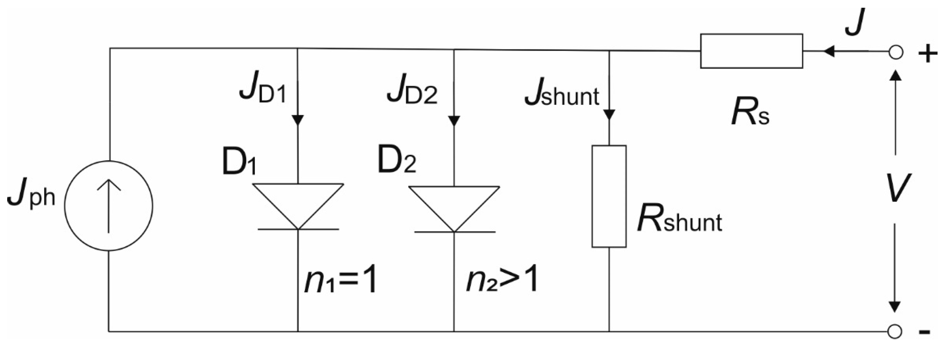
Under illumination, an ideal solar cell can be represented by a parallel circuit which consists of an ideal diode (
D1) and a constant current source of photogenerated current (
Jph). The improved equivalent circuit model, so called 2-diode model, is shown in
Figure 9 [
67,
68]. Equivalent circuit for solar cell under dark condition differs only in vanishing photogenerated current source J
ph.
The ideal diode
D1 represents the radiative recombination in the solar cell (perovskite layer), while the non-radiative recombination processes are represented by the diode
D2. In the equivalent circuit, two resistances are present: series
Rs and parallel
Rshunt, which have a high impact on solar cell performance, since they govern the shape and slopes of the
J–V characteristics. They can be calculated from the slope of the
J–V curve at the
Voc point (
Rs) and at
Jsc point (
Rshunt).
Rs represents the net effect of the ohmic loss and has its origin in the electrical resistance of contacts (ITO and gold in our PSC) and in the electrical dissipation, which is occurring in the layers of PSC (ETL, perovskite and HTL). In contrast,
Rshunt represents the leakage current loss induced by defects in the solar cell, such as traps and pinholes.
Rs mainly affects the
FF and
Jsc, while a low
Rshunt value results in a photovoltage loss and can affect the collected photocurrent. It is commonly known that a low
Rs and high
Rshunt are preferred in order to have highly efficient solar cells. The
J–V characteristic of the equivalent circuit can be described by the following equation [
36]
where
J1 and
J2 are the saturation current densities of the two diodes, respectively,
A is the area of the solar cell,
n1 and
n2 are the ideality factors of the two diodes.
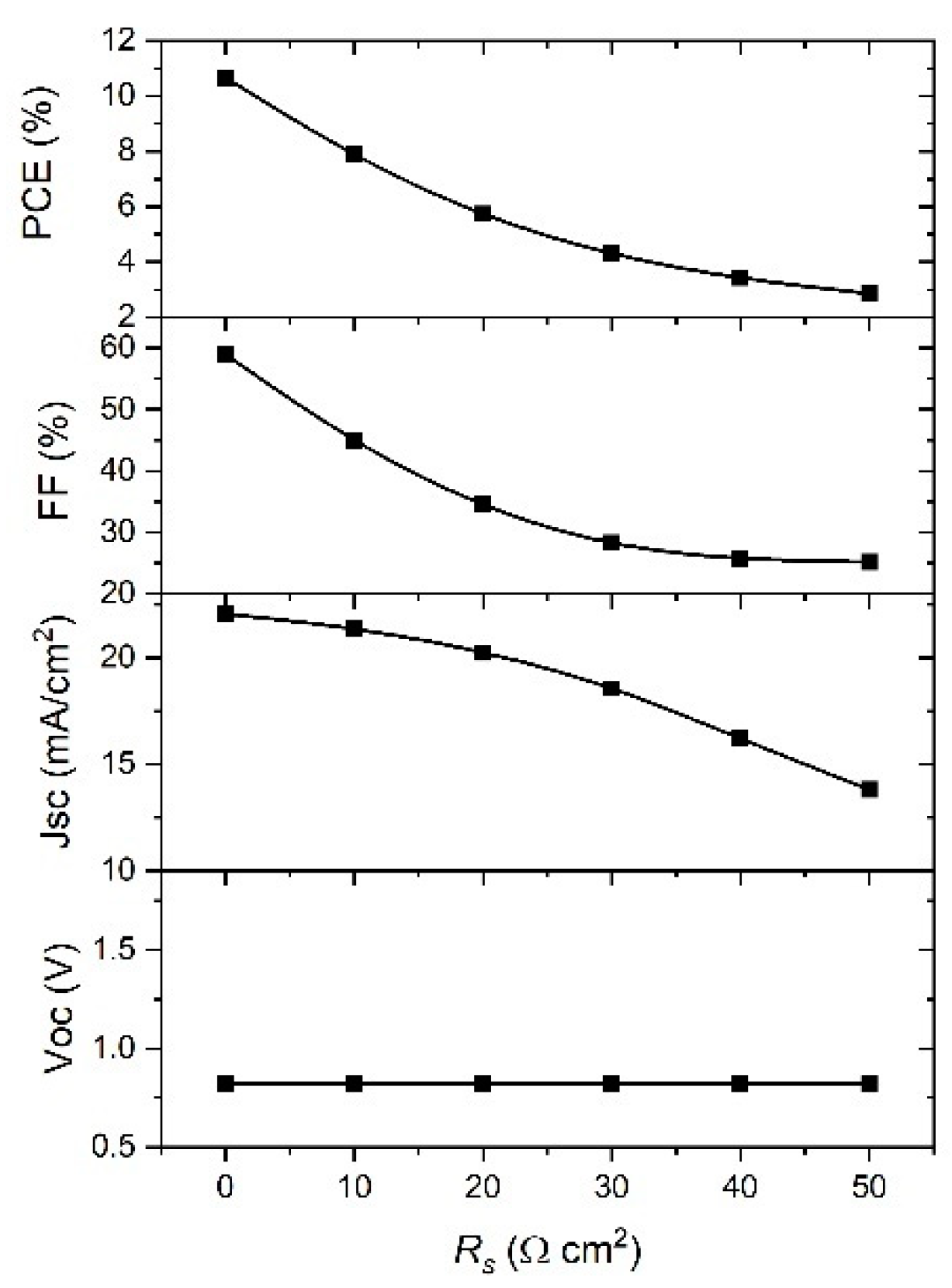
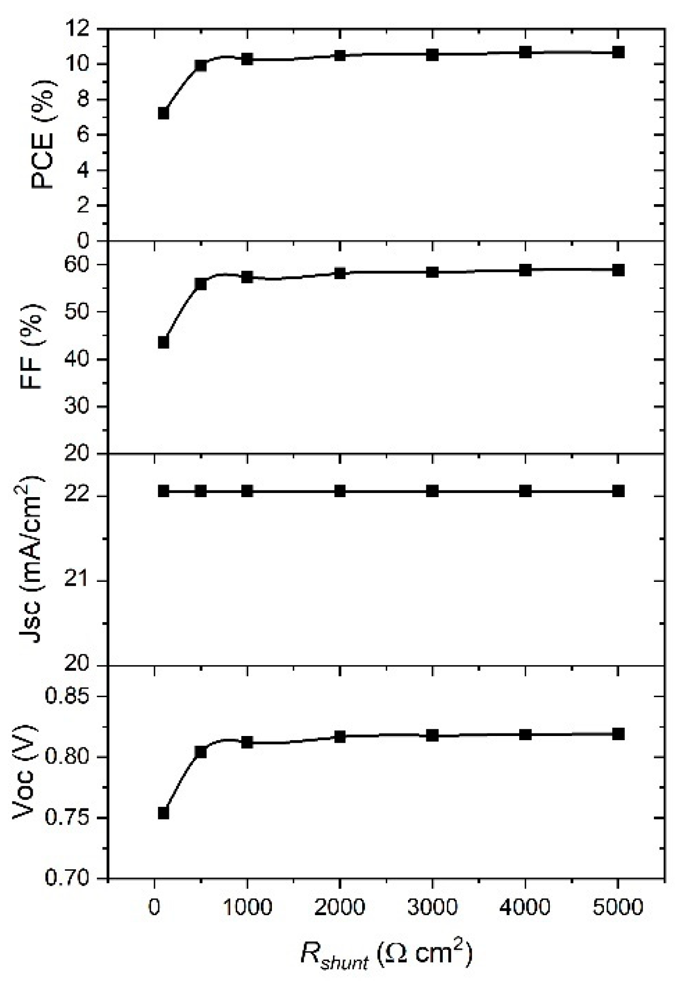
In order to understand the effect of
Rs and
Rshunt on the performance of PSCs, the SCAPS model was used with the range of their values 0–50 Ω cm
2 and 100–5000 Ω cm
2, respectively. The obtained simulation results are given in
Figure 10 and
Figure 11, and it is clear from the graph in
Figure 10 that the
Voc is not affected by the change of
Rs, while other parameters decreased with the increase in
Rs value; indeed, the
Jsc decreases slowly from 22 mA cm
−2 to less than 15 mA cm
−2. The
FF value was reduced by half, from 60% to less than 30%, while the
PCE decreased from 10% to approximately 3%. It can be observed from the results that PSC parameters are strongly affected by the change of
Rs, except the
Voc, meaning the best device performance will be for the lowest
Rs.
Considering the dependence of the PSC parameters on
Rshunt,
Figure 11 clearly shows that
Jsc is the parameter that is not affected by
Rshunt change. The rest of parameters show a significant increase when
Rshunt increased from 100 to 1000 Ω cm
−2, and they are saturated for higher values of
Rshunt. Therefore, the higher values of
Rshunt, the better performance of the device. From the best fit of the experimental
J–V curve (
Figure 2) we obtained the values for
Rs = 9 Ω cm
−2 and
Rshunt = 1000 Ω cm
−2. When we used the ideal values of
Rs and
Rshunt, and ran a simulation of our device, we achieved a significant improvement in
PCE from 7.25% to 10.8%.
There is one more issue in SCAPS model which can significantly affect the performance of the device through
Rs and
Rshunt, and this is the interface layer between ETL-perovskite and perovskite-HTL. The interface layer is a source of high concentration of defects, which can drastically decrease the device performance. In many studies [
56,
61], the initial parameter of defect concentration in interface layers is usually set around
Nt = 10
16–10
17 cm
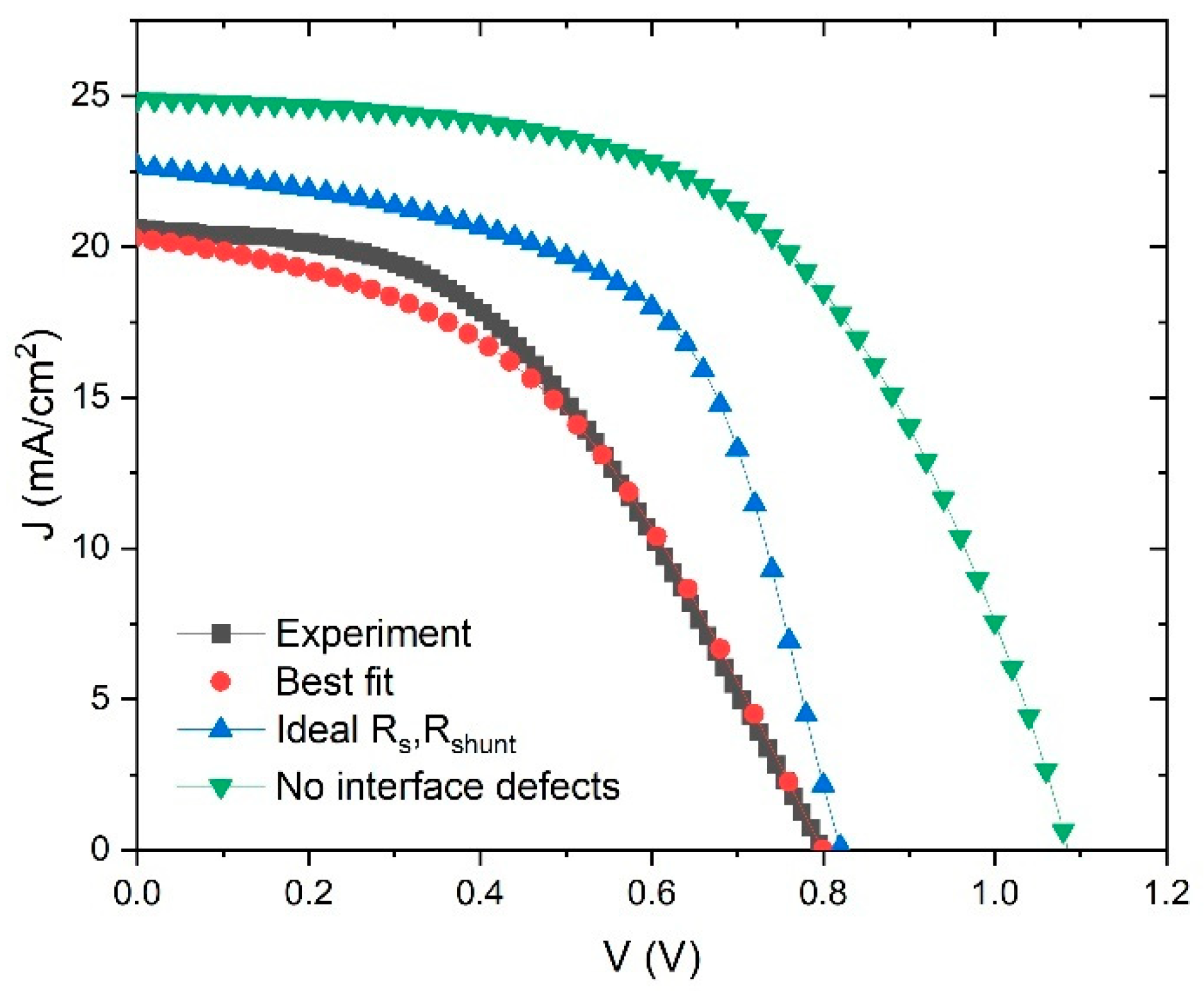
−3. We can simulate the reduction in defect concentration and study its influence on performance of the device, and this simulation can be seen in
Figure 12.
First,
Figure 12 shows the experimental and best fit
J–V curves, as in
Figure 2. In addition, there is a curve that describes an improvement in device parameters by taking the ideal values of
Rs and
Rshunt (
Voc = 0.82 V,
Jsc = 22.7 mA/cm
2,
FF = 58.2%,
PCE = 10.8%). We can improve these parameters even further by taking an ideal structure (no interface defects), but only for academic reasons, to see the theoretical limit of the device performance. In that case, the PSC parameters are:
Voc = 1.09 V,
Jsc = 24.9 mA/cm
2,
FF = 56.1% and
PCE = 15.17%. This means that, theoretically, our device has enough space to double its
PCE from 7.25% to 15%. One way to ensure better performance is to lower resistivity and decrease interface defects by improving structures of the device layers.
Therefore, it is possible to improve the PSC performances experimentally, mainly by influencing
Rs and
Rshunt. Experimentally, series resistance,
Rs, can be decreased by additives in HTL [
44,
45], by inserting the interlayers in PSCs [
46,
47,
49,
50], or by the composition of the perovskite layer [
48].
Since low
Rshunt is a consequence of pinholes formation and film porosity, it can be increased experimentally by solvents’ additives which eliminate formation of pinholes [
51], by the usage of a compact TiO
2 blocking layer below the mesoporous TiO
2 film [
52], or by passivation materials that block shunt pathways [
53,
54].
4. Conclusions
SCAPS-1D software was used to successfully simulate the J–V characteristics of the experimentally measured perovskite solar cell with an ITO/TiO2/Perovskite/Spiro-MeOTAD/Au structure. The values obtained by modelling (Jsc = 20.29 mA/cm2, Voc = 0.80 V, FF = 44.68% and PCE = 7.25%) were similar to measured values (Jsc = 20.60 mA/cm2, Voc = 0.8 V, FF = 45.51% and PCE = 7.35%).
Acceptor doping concentrations of the perovskite layer were optimized by simulations of the value NA = 1016 cm−3. As a result of the simulation, when the thickness increased above 800 nm, the PCE remained invariable.
It was shown that the Voc is not affected by a change in Rs, while the other parameters decreased with the increase of Rs, so the best device performance will be for the lowest Rs. Regarding the Rshunt, Jsc is not affected by Rshunt change, while the rest of the parameters show a significant increase when Rshunt rose from 100 to 1000 Ω cm2, and they are saturated for higher values of Rshunt.
The reduction of the defect concentration in the interface between layers was also simulated to see its influence on the performance of the device, by taking the ideal values of Rs and Rshunt (no interface defects), so the theoretical limit of the device performance was obtained: Voc = 1.09 V, Jsc = 24.9 mA/cm2, FF = 56.1% and PCE = 15.17%. Therefore, theoretically, our device could double its PCE from 7.25% to 15%.
The results have shown that SCAPS-1D software can be used to adequately simulate non-ideal perovskite solar cells. In this regard, SCAPS can be used as a tool to study potential failure points of obtained perovskite solar cell and as a guide where and how to improve the device performance. Furthermore, the results have shown that, for the PSC experimentally prepared in this work, we can improve PCE mainly by influencing Rs and Rshunt. Taking into account the thermal stability of the material, the Rb0.05Cs0.1FA0.85PbI3 perovskite is a very promising material for further studies.
