
Changes in Permittivity of the Piezoelectric Material PVDF as Functions of the Electrical Field and Temperature


Abstract
:1. Introduction
2. Materials and Methods
2.1. Basic Standard Equations for Piezoelectric Materials
2.1.1. Strain-Charge Form
2.1.2. Permittivity Calculation
2.2. Material Properties
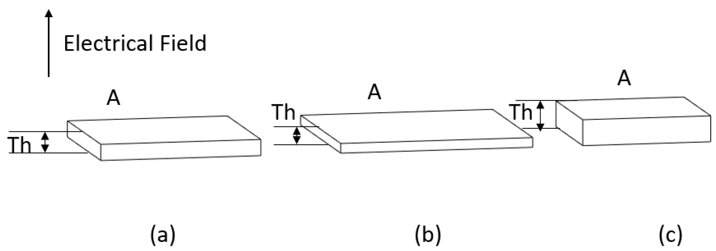
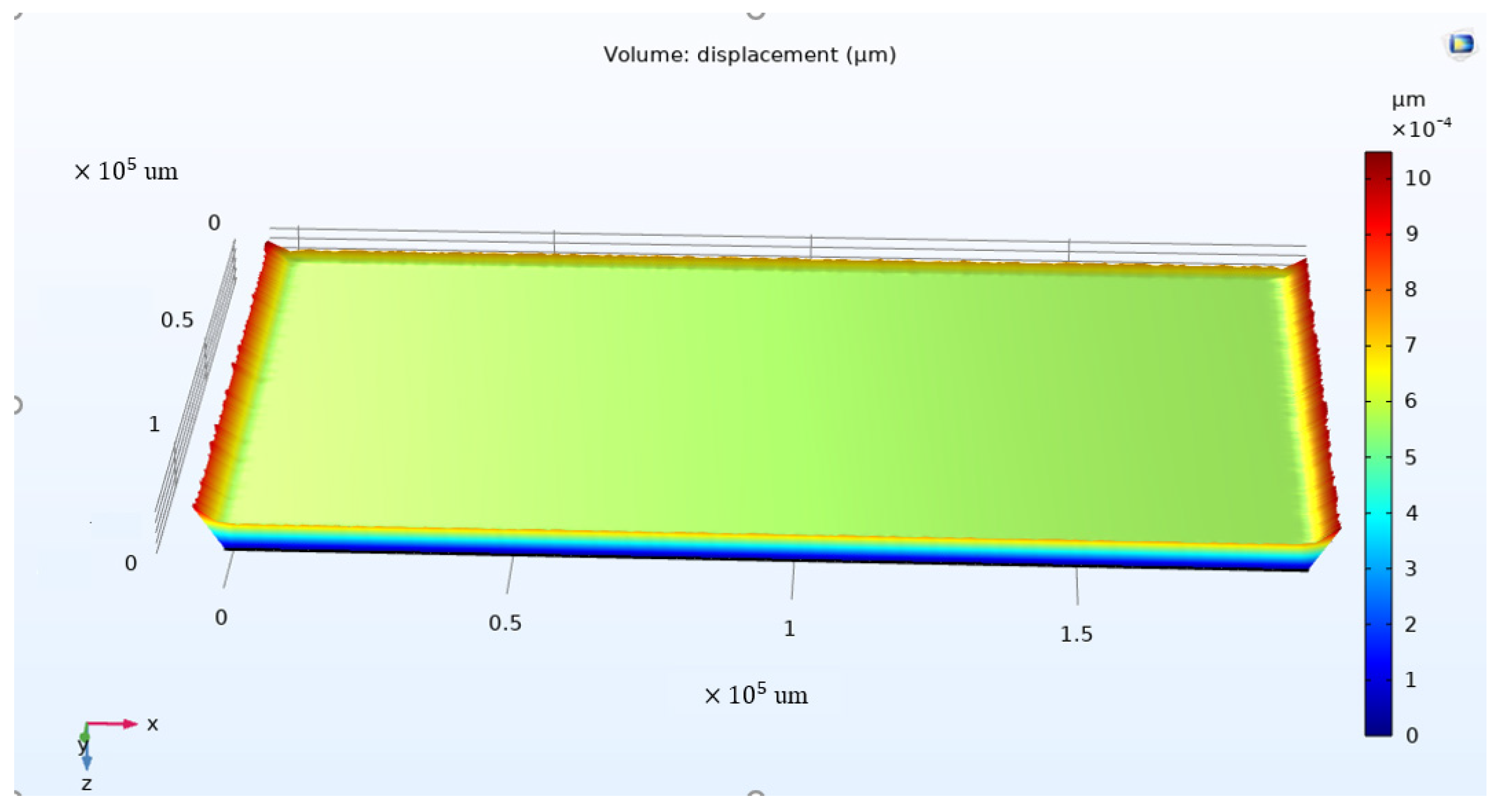
2.3. Simulation in COMSOL 5.6
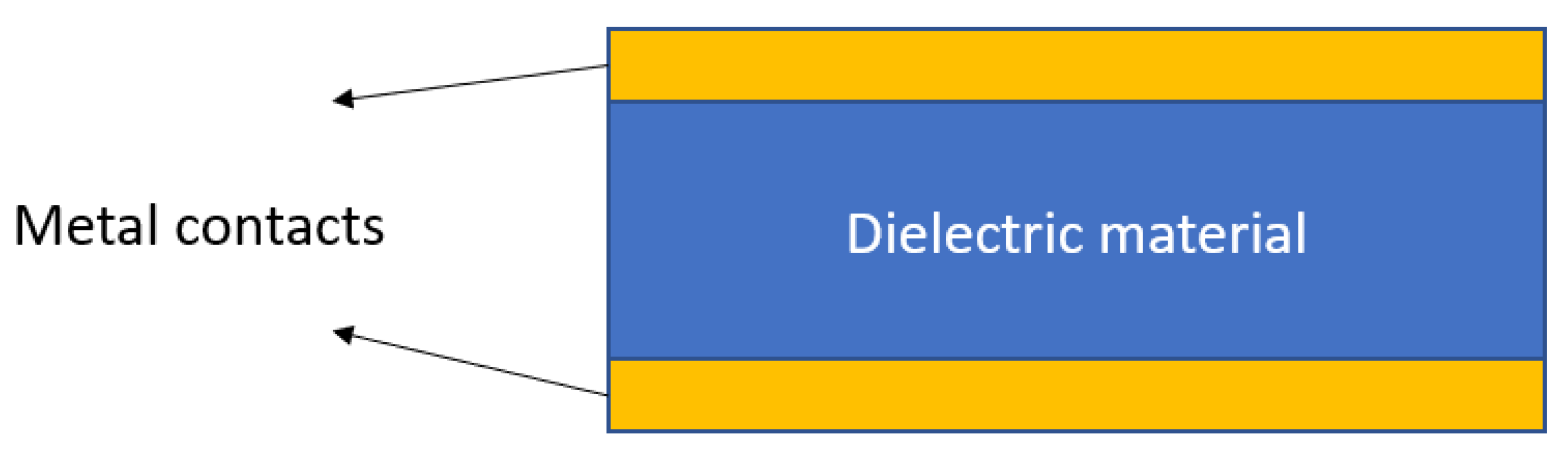
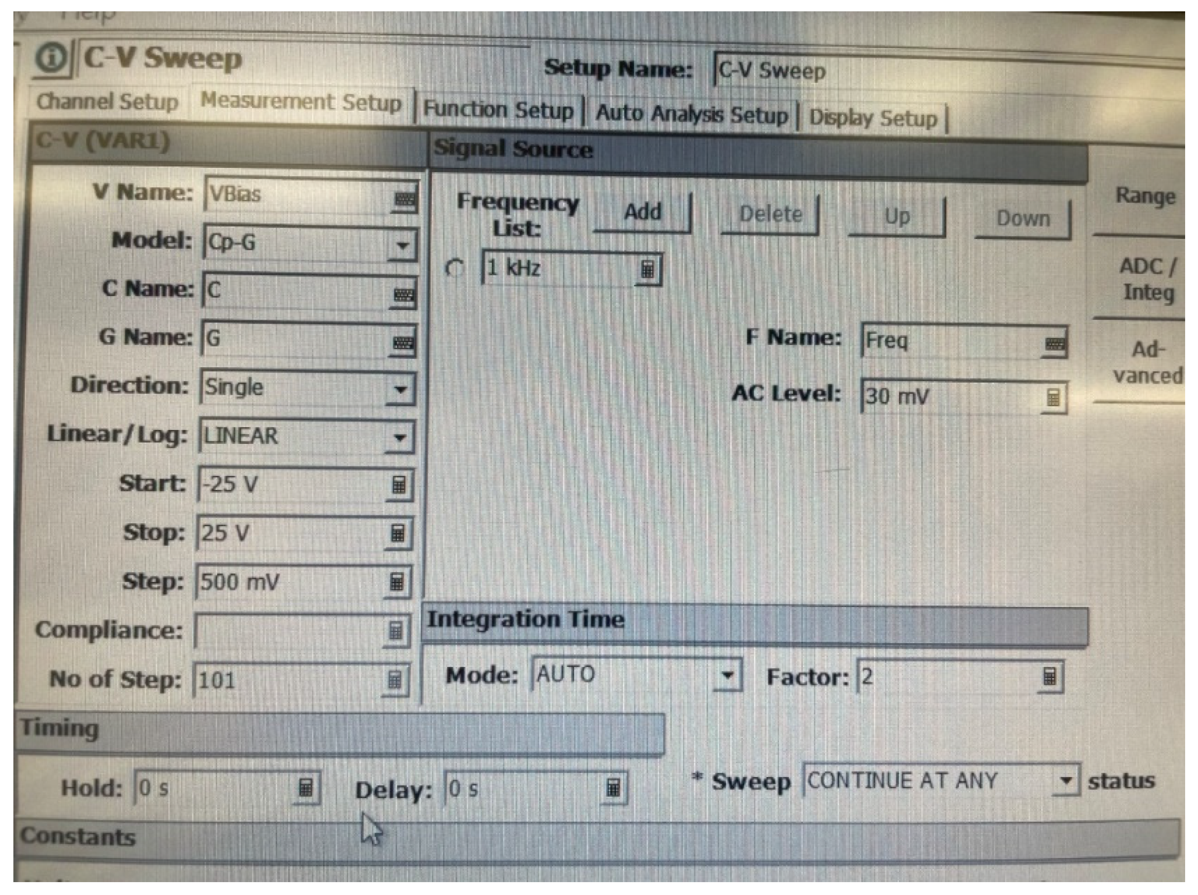
2.4. Experimental Measurement
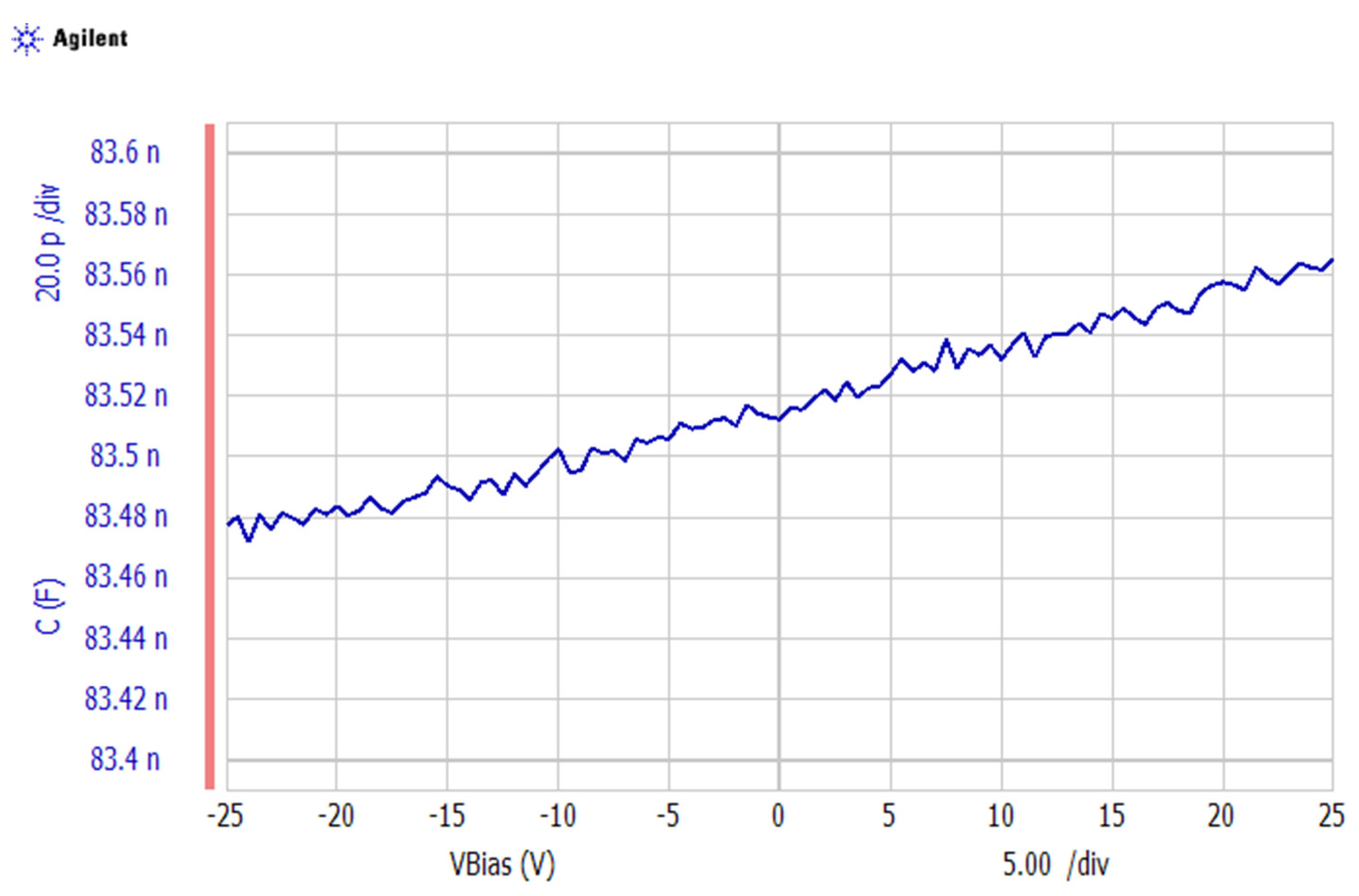
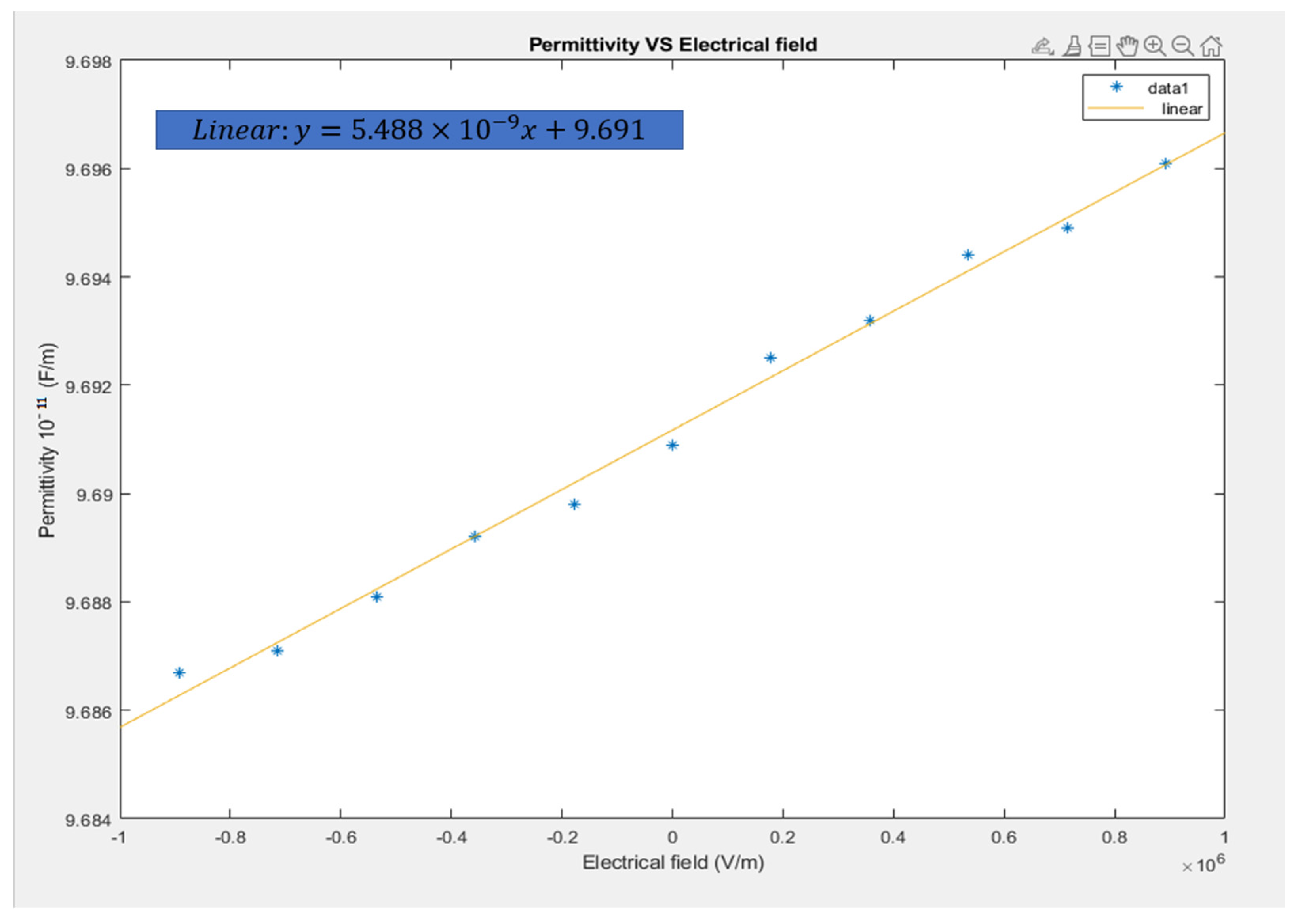
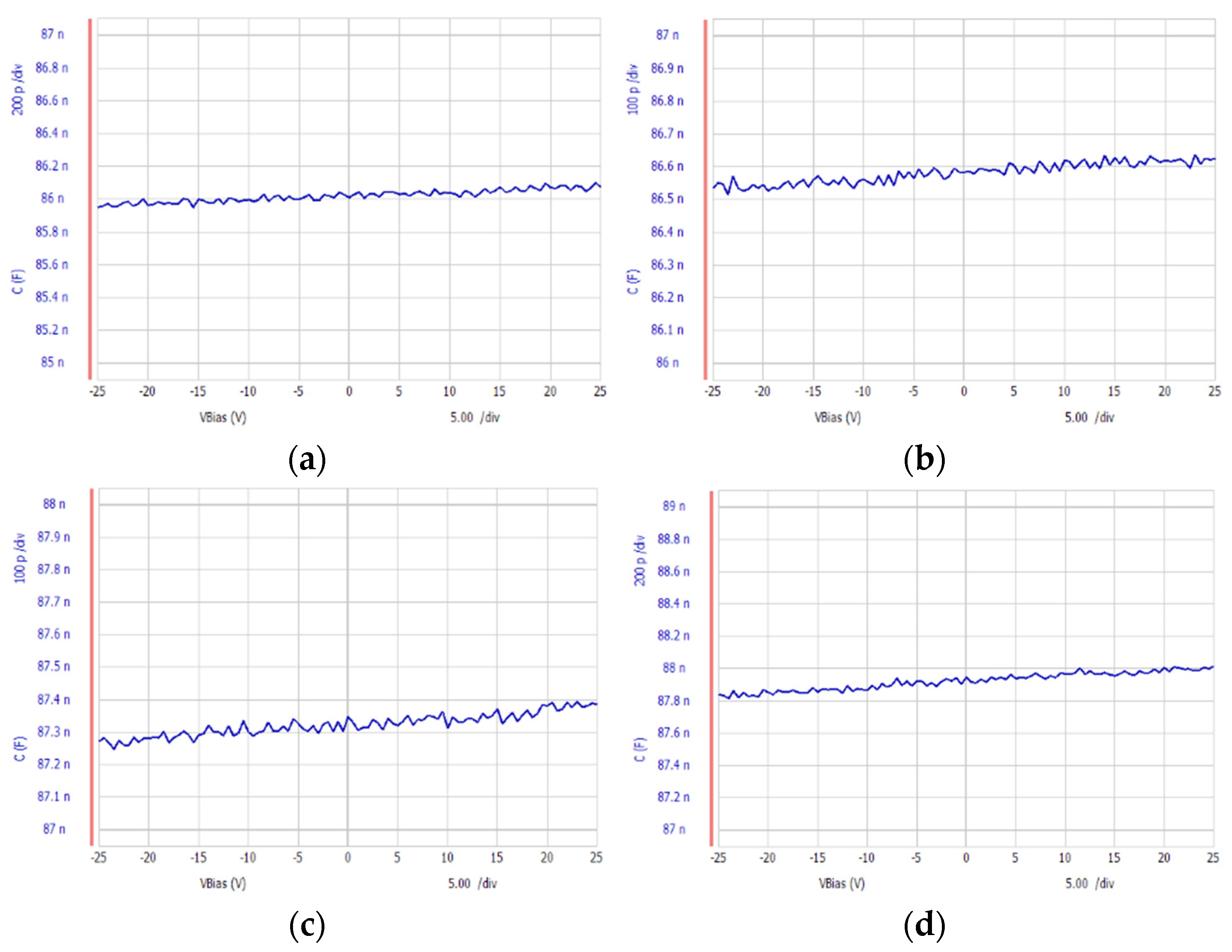
3. Results
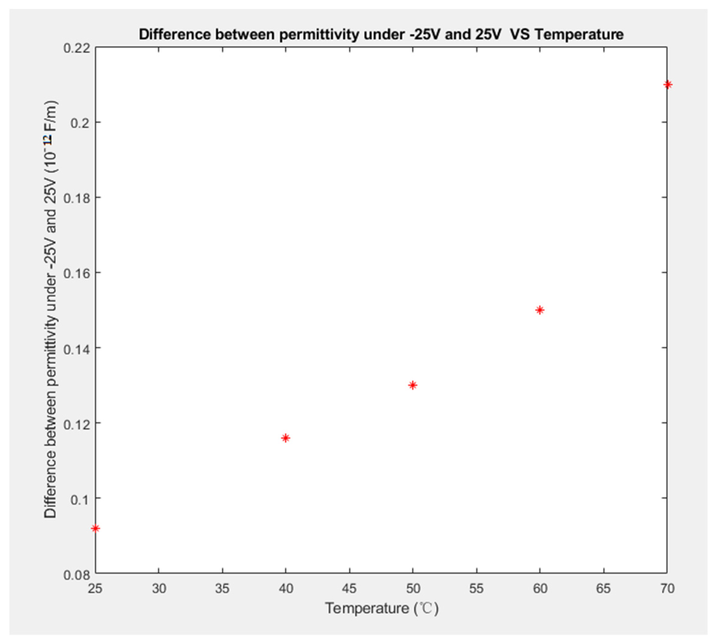
4. Discussion
Author Contributions
Funding
Institutional Review Board Statement
Informed Consent Statement
Data Availability Statement
Acknowledgments
Conflicts of Interest
References
- Liu, C. Piezoelectric Sensing and Actuation. In Foundations of MEMS; Pearson Prentice Hall: Upper Saddle River, NJ, USA, 2006; pp. 245–246. [Google Scholar]
- Dong, B.; Zaghloul, M. Generation and enhancement of surface acoustic waves on a highly doped p-type GaAs substrate. Nanoscale Adv. 2019, 1, 3537–3546. [Google Scholar] [CrossRef] [Green Version]
- Sukesha Vig, R.; Kumar, N. Effect of Electric Field and Temperature on Dielectric Constant and Piezoelectric Constant of Piezoelectric Materials: A Review. Integr. Ferroelectr. 2015, 167, 154–175. [Google Scholar] [CrossRef]
- Dong, B.; Afanasev, A.; Johnson, R.; Zaghloul, M. Enhancement of Photoemission on p-Type GaAs Using Surface Acoustic Waves. Sensors 2020, 20, 2419. [Google Scholar] [CrossRef] [PubMed]
- Hinchet, R.; Khan, U.; Falconi, C.; Kim, S.W. Piezoelectric properties in two-dimensional materials: Simulations and experiments. Mater. Today 2018, 21, 611–630. [Google Scholar] [CrossRef]
- Zhou, Y. Design and Simulation of SAW-Driven Drug Delivery Device. Master’s Thesis, The George Washington University, Washington, DC, USA, 2020. [Google Scholar]
- Sukesha, R.; Kumar, N. Variation of piezoelectric coefficient and dielectric constant with electric field and temperature: A review. In Proceedings of the 2014 Recent Advances in Engineering and Computational Sciences (RAECS), Panjab, India, 6–8 March 2014. [Google Scholar]
- Park, W.; Yang, J.S.; Kang, C.G.; Lee, Y.S.; Hwang, H.J.; Cho, C.; Lim, S.K.; Kang, S.C.; Hong, W.K.; Lee, S.K.; et al. Characteristics of a pressure sensitive touch sensor using a piezoelectric PVDF-TrFE/MoS2 stack. Nanotechnology 2013, 24, 475501. [Google Scholar] [CrossRef] [PubMed] [Green Version]
- Abbasipour, M.; Khajavi, R.; Yousefi, A.A.; Yazdanshenas, M.E.; Razaghian, F. The piezoelectric response of electrospun PVDF nanofibers with graphene oxide, graphene, and halloysite nanofillers: A comparative study. J. Mater. Sci. Mater. Electron. 2017, 28, 15942–15952. [Google Scholar] [CrossRef]
- Wang, S.; Dong, B.; Zaghloul, M. Interface Electronics Design for Wireless Generation of Surface Acoustic Wave Utilized in Wearable Drug Delivery Application. In Proceedings of the 2020 XXXIIIrd General Assembly and Scientific Symposium of the International Union of Radio Science (URSI GASS), Rome, Italy, 29 August–5 September 2020. [Google Scholar]
- Rajala, S.; Lekkala, J. Film-Type Sensor Materials PVDF and EMFi in Measurement of Cardiorespiratory Signals—A Review. IEEE Sens. J. 2012, 12, 439–446. [Google Scholar] [CrossRef]
- Jacobs, J.L.; Embree, P.; Glei, M.; Christensen, S.; Sullivan, P.K. Characterization of a novel heart and respiratory rate sensor. Proceedings of The 26th Annual International Conference of the IEEE Engineering in Medicine and Biology Society, San Francisco, CA, USA, 1–5 September 2004. [Google Scholar]
- Choi, S.; Jiang, Z. A novel wearable sensor device with conductive fabric and PVDF film for monitoring cardiorespiratory signals. Sens. Actuators A Phys. 2006, 128, 317–326. [Google Scholar] [CrossRef]
- Ansourian, M.N.; Dripps, J.H.; Jordan, J.R.; Beattie, G.J.; Boddy, K. A transducer for detecting foetal breathing movements using PVDF film. Physiol. Meas. 1993, 14, 365–372. [Google Scholar] [CrossRef] [PubMed]
- Chen, W.; Zhu, X.; Nemoto, T.; Kanemitsu, Y.; Kitamura, K.; Yamakoshi, K. Unconstrained detection of respiration rhythm and pulse rate with one under-pillow sensor during sleep. Med. Biol. Eng. Comput. 2005, 43, 306–312. [Google Scholar] [CrossRef] [PubMed]
- Niizeki, K.; Nishidate, I.; Uchida, K.; Kuwahara, M. Unconstrained cardiorespiratory and body movement monitoring system for home care. Med. Biol. Eng. Comput. 2005, 43, 716–724. [Google Scholar] [CrossRef] [PubMed]
- Bai, P.; Wang, S.; Jia, J.; Wang, H.; Yang, W. Effect of BaTiO3 nanowire on effective permittivity of the PVDF composites. AIP Adv. 2021, 11, 045018. [Google Scholar] [CrossRef]
- Piezoelectric Materials: Understanding the Standards. Available online: https://www.comsol.com/blogs/piezoelectric-materials-understanding-standards/ (accessed on 12 June 2021).
- Ahmad, M.A.; Allataifeh, A. Electrical extraction of piezoelectric constants. Heliyon 2018, 4, e00910. [Google Scholar] [CrossRef] [PubMed] [Green Version]
- Piezo Film Sheets from TE Connectivity. Available online: https://www.cdiweb.com/portalproductdetail.aspx?ProdId=185115&ManufId=355 (accessed on 29 September 2021).


Publisher’s Note: MDPI stays neutral with regard to jurisdictional claims in published maps and institutional affiliations. |
© 2021 by the authors. Licensee MDPI, Basel, Switzerland. This article is an open access article distributed under the terms and conditions of the Creative Commons Attribution (CC BY) license (https://creativecommons.org/licenses/by/4.0/).
Share and Cite
Zhou, Y.; Zaghloul, M. Changes in Permittivity of the Piezoelectric Material PVDF as Functions of the Electrical Field and Temperature. Materials 2021, 14, 5736. https://doi.org/10.3390/ma14195736
Zhou Y, Zaghloul M. Changes in Permittivity of the Piezoelectric Material PVDF as Functions of the Electrical Field and Temperature. Materials. 2021; 14(19):5736. https://doi.org/10.3390/ma14195736
Chicago/Turabian StyleZhou, You, and Mona Zaghloul. 2021. "Changes in Permittivity of the Piezoelectric Material PVDF as Functions of the Electrical Field and Temperature" Materials 14, no. 19: 5736. https://doi.org/10.3390/ma14195736
APA StyleZhou, Y., & Zaghloul, M. (2021). Changes in Permittivity of the Piezoelectric Material PVDF as Functions of the Electrical Field and Temperature. Materials, 14(19), 5736. https://doi.org/10.3390/ma14195736