Article

Regulation of Hole Concentration and Mobility and First-Principle Analysis of Mg-Doping in InGaN Grown by MOCVD

1
Institute of Semiconductors, Chinese Academy of Sciences, Beijing 100083, China
2
Microsystem and Terahertz Research Center, China Academy of Engineering Physics, Chengdu 610200, China
3
Hangzhou Global Scientific and Technological Innovation Center, Zhejiang University, Hangzhou 311200, China
4
Lishui Zhongke Semiconductor Material Co., Ltd., Lishui 323000, China
5
Department of Physics, School of Science, Wuhan University of Technology, Wuhan 430070, China
*
Author to whom correspondence should be addressed.
Materials 2021, 14(18), 5339; https://doi.org/10.3390/ma14185339
Submission received: 31 August 2021 / Revised: 10 September 2021 / Accepted: 13 September 2021 / Published: 16 September 2021
(This article belongs to the Section Materials Physics)

Abstract

:
This work studied the regulation of hole concentration and mobility in p-InGaN layers grown by metalorganic chemical vapor deposition (MOCVD) under an N-rich environment. By adjusting the growth temperature, the hole concentration can be controlled between 6 × 10¹⁷/cm3 and 3 × 10¹⁹/cm3 with adjustable hole mobility from 3 to 16 cm2/V.s. These p-InGaN layers can meet different requirements of devices for hole concentration and mobility. First-principles defect calculations indicate that the p-type doping of InGaN at the N-rich limiting condition mainly originated from Mg substituting In (MgIn). In contrast with the compensation of nitrogen vacancy in p-type InGaN grown in a Ga-rich environment, the holes in p-type InGaN grown in an N-rich environment were mainly compensated by interstitial Mg (Mgi), which has very low formation energy.

1. Introduction

InGaN alloys are attractive semiconductor materials due to their tunable bandgap energy (Eg) range from 0.65 to 3.4 eV. Thin undoped InGaN layers are widely used in light-emitting diodes (LEDs) and laser diodes (LDs) for lighting, displays and communication [1,2,3]. Due to the high absorption coefficient (~105 cm−1) and high radiation resistance [4], thick intrinsic InGaN layers are also prospective candidates for solar cells [5]. In green LDs, thick InGaN layers are used as a waveguiding layer with the inherent benefit of a higher confinement factor [6]. Moreover, the valance band maximum (VBM) of InGaN alloys is higher than that of GaN, which reduces the active energy of Mg and contributes to a high hole concentration in gallium nitrides. p-InGaN layers with thickness beyond 100 nm were reported in solar cells [7] and heterojunction bipolar transistors (HBTs) [8] as the hole-injection and p-type conduction layers.
Many scholars focused on improving the crystal quality of p-type InGaN layers to obtain a large hole concentration and maintain high hole mobility [9,10,11,12]. A hole concentration of 7.7 × 10¹⁷/cm3 was achieved on an Mg-doped In0.04Ga0.96N grown by molecular beam epitaxy (MBE) [13]. By reducing lattice mismatch, a p-type In0.18Ga0.82N with a hole concentration up to 3 × 1019 cm−3 was grown on a GaN substrate by plasma-assisted MBE (PA-MBE) [14]. MOCVD was also used to grow a p-type In0.22Ga0.78N layer with a hole concentration of 5 × 1018 cm−3 [15]. However, these reported hole mobilities are limited to less than 10 cm2/V.s. Not all devices need to maintain high mobility at a higher hole concentration. For example, devices using p-type layers as hole injection layers, high hole concentration and high mobility are both needed to form large hole current. In addition to these, there are some devices that only need high hole concentration, such as p-type E-mode high electron mobility transistors (HEMTs). High hole concentration is useful to deplete two-dimensional electron gas, resulting in high threshold voltage. However, it does not need high hole mobility, which can lead to a large gate current. It is significant to regulate the hole concentration and mobility within a certain range, so as to meet the needs of different devices.
The main factors affecting hole concentration and mobility in p-type InGaN are as follows. First, V-pits form easily in InGaN layers due to a large lattice mismatch and large thermal expansion coefficient between InN and GaN [16]. V-pits can act as traps of holes, which decreases the hole concentration. In addition, the scattering of V-pits reduces hole mobility [17]. Second, there is a high concentration of background electrons in InGaN layers [18]. Positively charged N vacancies (VN) are considered to be the source of the high background-electron concentration because of the low formation energy in Ga-rich growth conditions [19]. However, reaction chambers of MOCVD usually present as an N-rich environment because the V/III ratio is usually in the order of thousands during the growth of gallium nitrides. The formation energy of VN is high in N-rich environments [20]. Other defects that can act as donor impurities to compensate holes in Mg-doped InGaN grown by MOCVD are still uncertain.
In this work, a 100 nm V-pit-free p-InGaN layer on a sapphire substrate was grown by MOCVD. By adjusting the growth temperature, the hole concentration could be controlled between 6 × 10¹⁷/cm3 and 3 × 10¹⁹/cm3 with adjustable hole mobility of 3 to 16 cm2/V.s. Mesoscopic defects such as spiral mounds and V-pits originated from the screw dislocation core. First-principles defect calculations were carried out to study defects in an Mg-doped InGaN layer at N-rich limit conditions. The results indicate that the p-type doping of InGaN mainly originated from the process of Mg substituting In (MgIn). For p-InGaN grown in the N-rich environment, native defects compensating holes were interstitial Mg (Mgi) instead of VN in the p-InGaN grown in the Ga-rich environment.

2. Materials and Methods

Under the same pressure of 150 torr, four 100 nm thick samples were grown by MOCVD on 2 inch c-plane sapphire substrates at 790 °C (Sample A), 800 °C (Sample B), 810 °C (Sample C) and 820 °C (Sample D). Triethylgallium (TEGa), trimethylindium (TMIn), bis-cyclopentadienyl-magnesium (Cp2Mg) and ammonia (NH3) were used as the precursors for Ga, In, Mg and N. Before the InGaN layers, 2 µm thick undoped GaN templates were grown on sapphire. The growth rate of the p-InGaN was about 1 nm per min, and the flux of Cp2Mg was 30 sccm for all the samples. Four p-InGaN layers were grown at 820 °C with different growth times of 5, 10, 20 and 50 min. The indium compositions of the InGaN layers were estimated by high-resolution X-ray diffraction (HR-XRD). Surface morphologies of all samples were revealed by atomic force microscopy (AFM, Veeco D3100, New York, NY, USA) with a scan area of 5 × 5 μm2. These samples were processed into Vander Pauw geometries for Hall effect measurements at room temperature (RT) in order to test hole concentration and mobility.

3. Results and Discussion

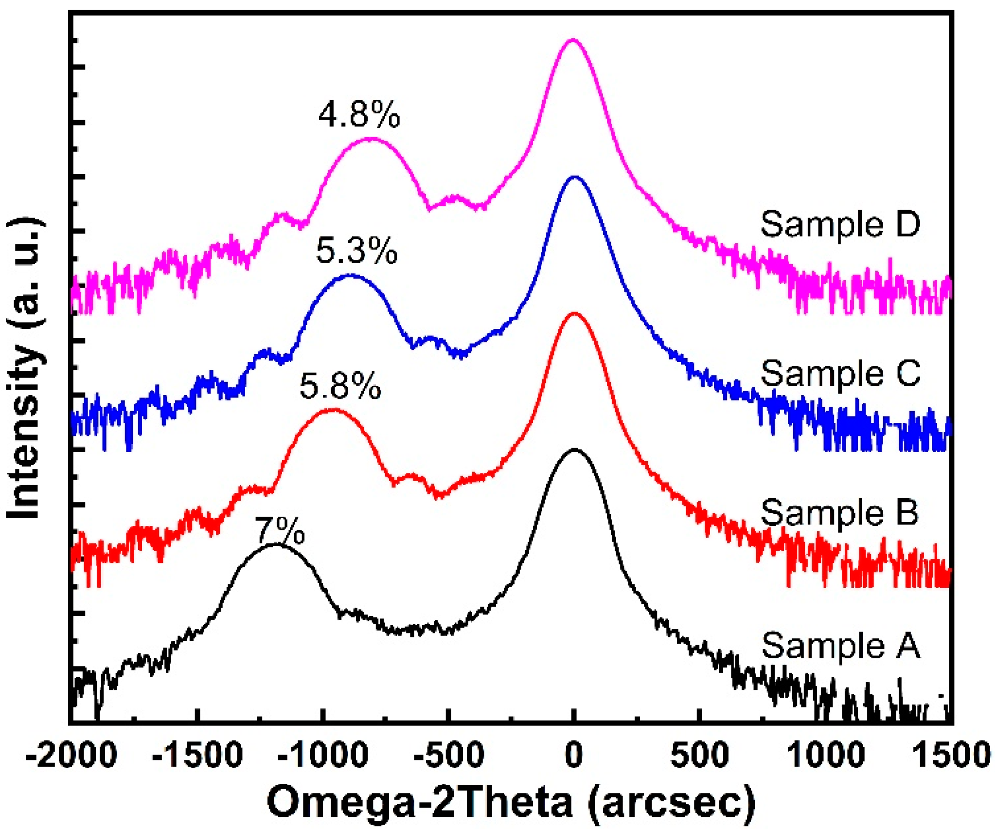
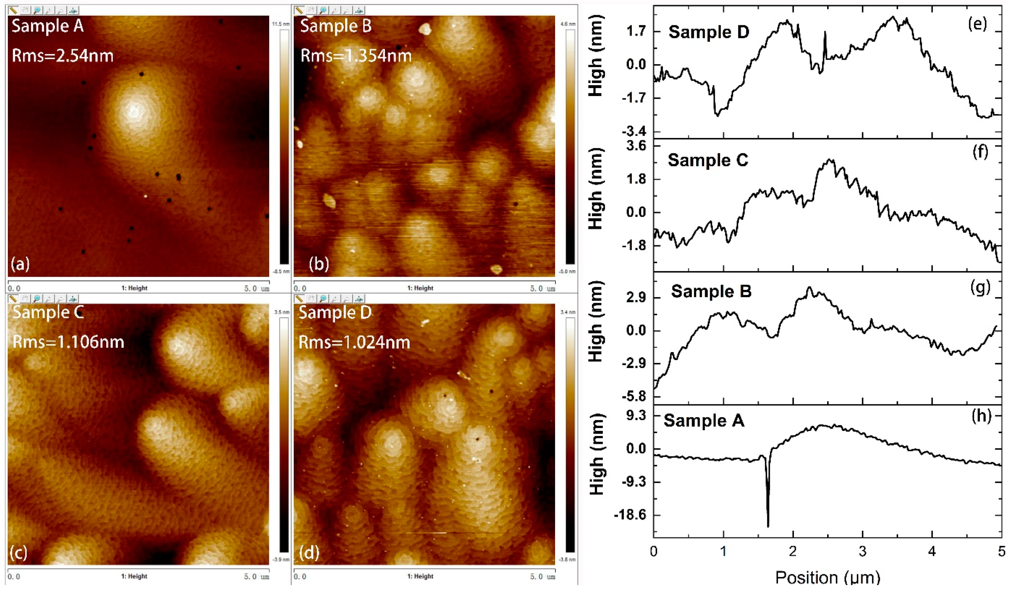
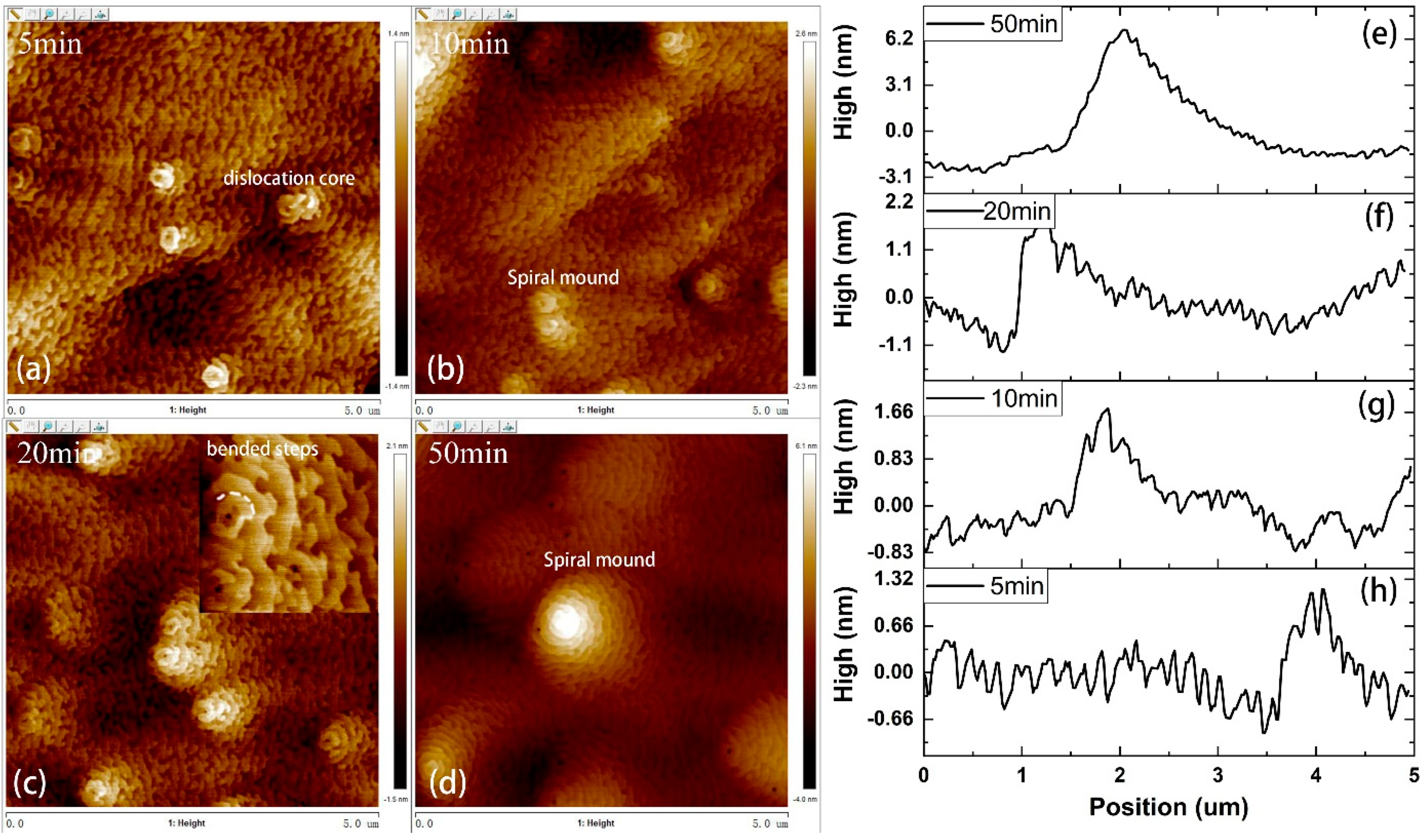
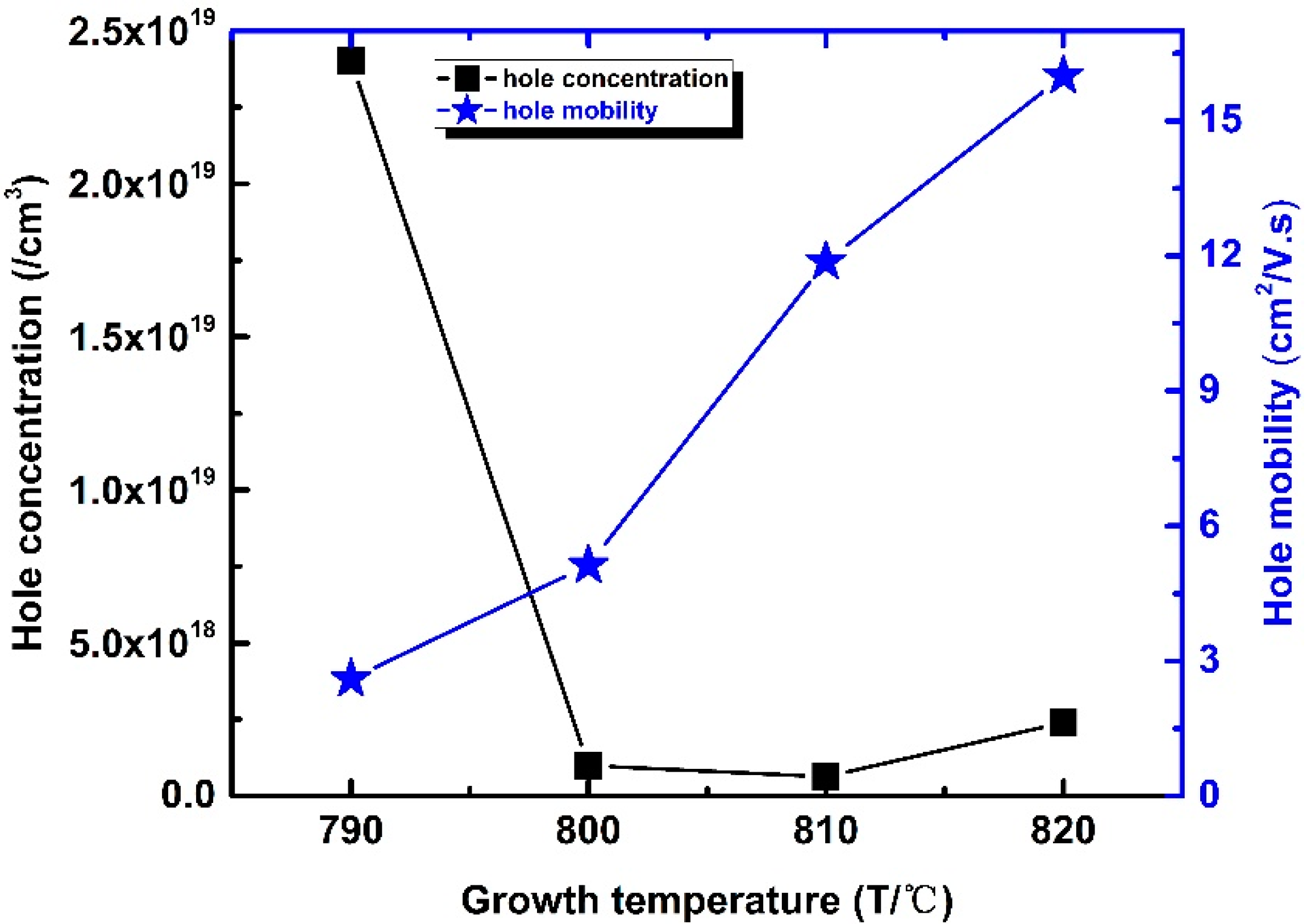
3.1. p-Type InGaN Growth

Figure 1 shows the ω-2θ scan rocking curves of p-InGaN layers under different growth temperature levels. Indium composition was calculated to be ~7%, 5.8%, 5.3% and 4.8% when the growth temperature was 790, 800, 810 and 820 °C, respectively, according to location of the InGaN peak. When the growth temperature increased, the indium composition was reduced due to the decreased incorporation rate of indium atoms. When the temperature exceeded 800 °C, the indium composition decreased to less than 6%. This is consistent with reported results based on the miscibility rate of InN in GaN, which revealed that the indium content was limited to less than 6% when the growth temperature was higher than 800 °C [21].
Figure 2 displays the AFM images (ad) and line scans (eh) of the images of the samples with a scan area of 5 × 5 μm2. Surface roughness was improved when the growth temperature increased. According to the line scans of the AFM images, the surface fluctuation of Samples A–D shrank. There were many V-pits with a density of ~1.08 × 10⁸/cm2 in the morphology of Sample A. In Samples B–D, the V-pits disappeared. In addition, for all the samples, some spiral mounds were observed on the surface.
In order to study the formation mechanism of the mesoscopic V-pits and spiral mound, four p-InGaN layers were grown at 820 °C with different growth times of 5, 10, 20 and 50 min. According to the calibrated growth rate of 1 nm/min by using the scanning electron microscope (SEM, S-4800, made in Japan) of the cross-section of Sample D, we determine that the thickness of the four InGaN layers was 5, 10, 20 and 50 nm, respectively. The morphologies of these layers are shown in Figure 3a–d. The line scans of these AFM images for different InGaN layers are shown in Figure 3e–h. As growth time increased, the surface fluctuation became larger. Several small spiral mounds could be observed on the surface of the p-InGaN under the growth time of 5 min. With increased growth time, the size of the spiral mounds increased, while the number of spiral mounds remained the same. Two spiral mounds are enlarged in Figure 3c. A dislocation core was observed in the spiral mound and the step bend around the dislocation core. During step-flow growth, one end of the step was pinned by screw dislocation. Then, the step curve around the dislocation core evolved into spiral mounds forming [22,23]. V-pits were only observed on the thickest p-InGaN layer, grown for 50 min, which indicated that these V-pits may have originated from threading dislocations (TDs) [24] or stacking faults in the InGaN layer. The TDs or stacking faults were generated by strain relaxation [25] due to the lattice mismatch between InGaN and GaN.
Figure 4 shows the hole concentration and mobility of all samples tested by Hall at RT. The hole concentration reduced from 2.4 × 10¹⁹/cm3 to 1.5 × 10¹⁸/cm3, and further to 6.3 × 10¹⁷/cm3 when the growth temperature increased from 790 to 800 and 810 °C. However, when the growth temperature continued to increase to 820 °C, the hole concentration increased to 2.4 × 10¹⁸/cm3 instead of decreasing. When the growth temperature increased from 790 to 820 °C, the indium content of InGaN alloys reduced, which led to a larger Eg. According to calculation:
Eg(InxGa1−xN) = xEg(In) + (1 − x)Eg(GaN) − bx(1 − x)
where Eg(InN) = 0.7 eV, Eg(GaN) = 3.42 eV, b = 1.3 eV, the band differences (ΔEg) among the four samples are given. Compared with Eg of Sample A, the Eg of Sample B increased by 46 meV. The ΔEg between Samples B and C was 19.3 meV, and the ΔEg between Samples C and D was 19.4 meV. The larger Eg caused the VBM to shift to a lower level, which increased the active energy of Mg in InGaN. Correspondingly, the hole concentration reduced. Due to the large ΔEg (46 meV) between Samples A and B, the hole concentration dynamically decreased. However, for Sample D, with the highest growth temperature and lowest In content, the hole concentration did not decrease, but increased. Defect density was reduced due to the high temperature and low In content, which resulted the hole concentration being enhanced.
Figure 4 shows that the hole mobility monotonously increased with an increase in temperature. The high hole concentration of Sample A led to low hole mobility, less than 3 cm2/V.s, due to serious carrier scattering and defect scattering. The result is consistent with reported data [26]. For Samples B and C, with a relatively low hole concentration and In content, hole mobility was increased thanks to the reduced carrier scattering and defect scattering. The hole mobility of Sample D reached 16 cm2/V.s, which is one of the highest values among those previously reported for p-InGaN layers with a hole concentration over 1 × 10¹⁸/cm3.
The four samples have different advantages. Samples A and B with high hole concentration and low mobility are suitable for p-type HEMTs to obtain high Vth with low gate current. Samples C and D with relatively high hole concentration and high mobility are undoubtedly attractive for some devices that need a high hole injection, such as LEDs and NPN-type HBTs.

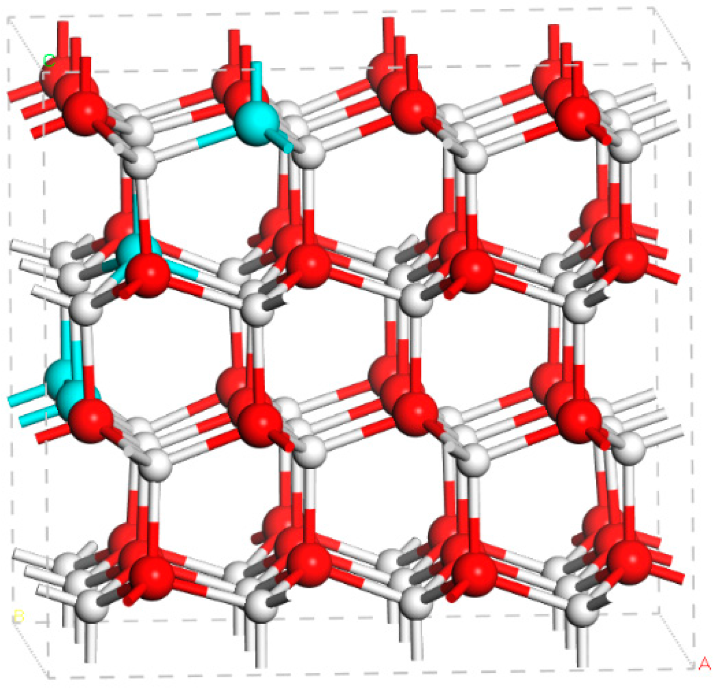
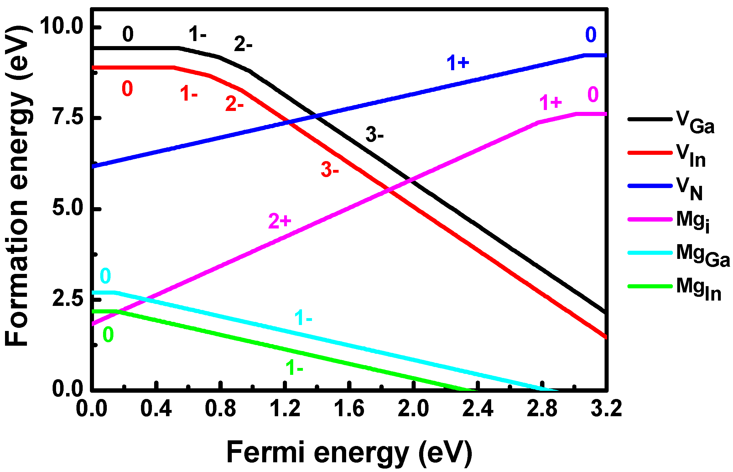
3.2. First-Principles Defect Calculations of p-Type InGaN

In order to investigate the microscopic defect properties of Mg in InGaN, we carried out first-principles defect calculations of Mg in the supercell of In4Ga44N48, which was approximate to the In composition of the above samples. A random In4Ga44N48 alloy was modeled by the SQS approach to determine cation site occupancies [27,28]. The produced atomic structure for the supercell of In4Ga44N48 is shown in Figure 5. First-principles calculations were carried out using projector augmented wave (PAW) pseudopotentials as implemented in the Vienna ab initio Simulation Package [29,30]. The 3D states of Ga and In atoms are included as valence electrons in the pseudopotentials. The plane-wave cut-off energies were set as 400 eV. Structural optimization was performed with the Perdew–Burke–Ernzerhof (PBE) exchange correlation functional. The atomic structures were optimized until changes in total energy were less than 1 × 10⁻⁵ eV per cell. During the electronic calculations, the screened hybrid density functional of Heyd, Scuseria and Ernzerhof (HSE06) was employed [31]. The fraction of the screened Fock exchange was set as 0.32, which resulted in bandgap energy for In4Ga44N48 of 3.18 eV. The Monkhorst–Pack scheme with a Γ-centered 2 × 2 × 2 special k-points mesh was adopted to sample the reciprocal space of the supercell [32].
In this work, defect configurations of interstitial Mg (Mgi), Mg substituting Ga (MgGa) and Mg substituting In (MgIn) were considered. Dominant intrinsic defects such as VN, VIn and VGa were considered. Formation energies of Mg and intrinsic defects were calculated by the mixed k-point scheme. The formation energy of defect α at the charge state q [ H f   ( α ,   q ) ] is calculated by [33,34]:
H f   ( α ,   q ) = E   ( α ,   q ) + n i μ i + q E F
where E   ( α ,   q ) = E ( α ,   q ) E ( InGaN ) + n i E i + q E V B M , E ( InGaN ) and E ( α ,   q ) are the total energies of the InGaN alloy and InGaN containing defect α with charge state q, respectively. n i is the number of atom i transferred from the supercell to the reservoir during the formation the defect, μ i is the chemical potential of the constituent i referenced to its elemental solid/gas with energy E i , EF is the Fermi energy referenced to the VBM of In4Ga44N48.
During the Mg doping in InGaN alloys, the accessible values of the chemical potentials μ i are limited by a series of requirements [35]. Firstly, the values of μ i are limited to those values that maintain a stable In4Ga44N48 alloy:
4 μ I n + 44 μ Ga + 48 μ N = H f   ( In 4 Ga 44 N 48 )
where H f   ( In 4 Ga 44 N 48 ) is the formation energy of In4Ga44N48 alloy. Secondly, to avoid the precipitation of elemental host phases and the elemental dopant, the values of μ i   are limited by:
μ I n     0 ,   μ G a     0 ,   μ N     0 ,   μ M g     0
Lastly, to avoid the formation of secondary phases, the values of μ i are limited by:
μ G a + μ N     H f   ( GaN ) , μ I n + μ N     H f   ( InN ) , 3 μ M g + 2 μ N     H f   ( Mg 2 N 3 )
where   H f   ( GaN ) , H f   ( InN ) and H f   ( Mg 2 N 3 ) are formation energies of InN, GaN and Mg3N2, respectively. The doping of Mg in InGaN alloys was carried out under the N-rich limit, which corresponds to μ N = 0 . Solving Equations (2)–(4), we obtained the values of μ for In, Ga, N and Mg of −1.3, 0, −0.18 and −1.50 eV, respectively.
The formation energies of Mg and dominant intrinsic defects in InGaN at the N-rich limit are shown in Figure 6. Firstly, the formation energies of VIn and MgIn were smaller than those of VGa and MgGa, respectively. The chemical potential of In was much smaller than that of Ga at the N-rich limit. It costs less energy for the removal and Mg substitution of In, compared to the case of Ga. Therefore, the p-type doping of InGaN at the N-rich limit mainly originated from MgIn. The (0/−) transition level of MgGa occurred at 0.14 eV above the VBM, which was lower than that of MgGa in GaN [36]. The defect level of MgGa is created from the host valence band. Since the VBM of InN was higher than that of GaN [37], alloying of In increased the VBM of GaN and lowered the defect level of MgGa in InGaN. The (0/−) transition level of MgIn was 0.16 eV above the VBM, which was slightly deeper than that of MgGa. This is because the 5p orbital energy of In is slightly higher than the 4p orbital energy of Ga. Mgi is a deep donor in InGaN, with the (2+/+) and (+/0) transition levels located at 0.40 and 0.17 eV below the conduction band minimum (CBM), respectively. As the Fermi energy of InGaN spreads throughout the bandgap, the charge state of VN changed from 1+ to 0. In GaN, the stable charge states of VN were 3+ and 1+ as the Fermi energy increased. VN created an empty defect level below the CBM and a half-occupied defect level above the VBM of GaN. Because the CBM of InN was lower than that of GaN, alloying of In into GaN lowered the energy of CBM. The empty defect level of VN moved to an energy level higher than the CBM of InGaN. Therefore, the defect level of VN in InGaN was only the half-occupied defect level above the VBM. Due to the N-rich limiting condition, the formation energy of VN was extremely high. The compensation of p-type doping for InGaN at the N-rich limiting condition was the formation of Mgi rather than VN. This result indicates that the p-type doping of InGaN grown by MOCVD cannot be enhanced by simply increasing the concentration of the Mg dopant. Once the concentration of Mg was larger than the sum concentration of MgIn and MgGa at the growth temperature, the formation of Mgi was not beneficial to the p-type doping of InGaN.

4. Conclusions

We grew 100 nm V-pit-free p-InGaN layers on a sapphire substrate by MOCVD. By adjusting the growth temperature, the hole concentration could be controlled between 6 × 10¹⁷/cm3 and 3 × 10¹⁹/cm3 with adjustable hole mobility of 3 to 16 cm2/V.s. A p-InGaN layer with a relatively high hole concentration of 2.4 × 10¹⁹/cm3 and low hole mobility of 3 cm2/V.s was obtained at 790 °C. It increased the threshold voltage and decreased the gate current for p-type E-HEMTs. A hole concentration of 2.4 × 10¹⁸/cm3 and high hole mobility of 16 cm2/V.s were achieved at 820 °C, which are attractive for devices requiring hole injection layers. Mesoscopic defects such as spiral mounds and V-pits originated from the screw dislocation core. First-principles defect calculations indicated that the p-type doping of InGaN in an N-rich limiting condition was mainly caused by MgIn. For p-type InGaN grown in an N-rich environment, hole compensation was the formation of Mgi rather than VN in the p-type doping of GaN grown at the Ga-rich environment. Results indicate that, during the p-type doping of InGaN by MOCVD, reducing Mgi is beneficial to increasing the hole concentration.

Author Contributions

Conceptualization, Y.Z.; methodology, X.T.; software, F.C.; formal analysis, Z.L. and S.Z.; investigation, L.Z. and R.W.; data curation, Z.C. and J.X. All authors have read and agreed to the published version of the manuscript.

Funding

The research is supported by the Science Challenge Project (grants no. TZ2018003 and TZ2016003), National Key R&D Program of China (no. 2017YFB0402900) and National Natural Science Foundation of China (grant no. 61674143).

Institutional Review Board Statement

Not applicable.

Informed Consent Statement

Not applicable.

Data Availability Statement

The data presented in this paper is available with request from the corresponding author.

Conflicts of Interest

The authors declare no conflict of interest.

References

  1. El-Mostafa, B.; Jeong, I.H. Electrical characterization and thermal admittance spectroscopy analysis of InGaN/GaN MQW blue LED structure. Electron. Mater. Lett. 2015, 11, 982–992. [Google Scholar]
  2. Lee, H.E.; Choi, J.H.; Lee, S.H.; Jeong, M.; Shin, J.H.; Joe, D.J.; Kim, D.; Kim, C.W.; Park, J.H.; Lee, J.H.; et al. Monolithic flexible vertical gan light-emitting diodes for a transparent wireless brain optical stimulator. Adv. Mater. 2018, 30, 1800649. [Google Scholar] [CrossRef]
  3. Lin, R.; Liu, X.; Zhou, G.; Qian, Z.; Cui, X.; Tian, P. InGaN Micro-LED Array Enabled Advanced Underwater Wireless Optical Communication and Underwater Charging. Adv. Opt. Mater. 2021, 9, 2002211. [Google Scholar] [CrossRef]
  4. Balakrishnam, R.J.; Andrew, G.M.; Muhammad, J.; Nikolai, N.F.; Robert, L.O.; Ian, T.F.; Christiana, B.H. Design and Realization of Wide-Band-Gap (∼2.67 eV) InGaN p-n Junction Solar Cell. IEEE Electron Device Lett. 2010, 31, 32–34. [Google Scholar]
  5. Omkar, J.; Ian, F.; Christiana, H.; Sarah, K. Design and characterization of GaN/InGaN solar cells. Appl. Phys. Lett. 2007, 91, 132117. [Google Scholar]
  6. Muzio, G.; Turski, H.; Siekacz, M.; Sawicka, M.; Skierbiszewski, C. Waveguide design for long wavelength ingan based laser diodes. Acta Phys. Pol. Ser. A 2012, 122, 1031–1033. [Google Scholar] [CrossRef]
  7. Mu-Tao, C.; Wen-Yih, L.; Ray-Hua, H.; Tsung-Yen, T.; Tsai-Bau, W.; Shu-Ping, L.; Ming-Hsien, W.; Ray-Ming, L. Growth and Characterization of p-InGaN/i-InGaN/n-GaN Double-Heterojunction Solar Cells on Patterned Sapphire Substrates. IEEE Electron Device Lett. 2011, 32, 922–924. [Google Scholar]
  8. Shen, S.C.; Dupuis, R.D.; Lochner, Z.; Lee, Y.C.; Kao, T.T.; Zhang, Y.; Kim, H.J.; Ryou, J.H. Working toward high-power GaN/InGaN heterojunction bipolar transistors. Semicond. Sci. Technol. 2013, 28, 074025. [Google Scholar] [CrossRef]
  9. Wang, X.; Che, S.B.; Ishitani, Y.; Yoshikawa, A. Systematic study on p-type doping control of InN with different Mg concentrations in both In and N polarities. Appl. Phys. Lett. 2007, 91, 242111. [Google Scholar] [CrossRef]
  10. Deng, Q.; Wang, X.; Xiao, H.; Wang, C.; Yin, H.; Chen, H.; Lin, D.; Jiang, L.; Feng, C.; Li, J.; et al. Comparison of as-grown and annealed GaN/InGaN:Mg samples. J. Phys. D-Appl. Phys. 2011, 44, 345101. [Google Scholar] [CrossRef]
  11. Chen, P.; Chen, C.H.; Chang, S.J.; Su, Y.K.; Chang, P.C.; Huang, B.R. High hole concentration of p-type InGaN epitaxial layers grown by MOCVD. Thin Solid Film. 2006, 498, 113–117. [Google Scholar] [CrossRef]
  12. Kuo, D.H.; Tuan, T.; Li, C.C.; Yen, W.C. Electrical and structural properties of Mg-doped InxGa1−xN (x ≤ 0.1) and p-InGaN/n-GaN junction diode made all by RF reactive sputtering. Mater. Sci. Eng. B 2015, 193, 13–19. [Google Scholar] [CrossRef]
  13. Chen, X.; Matthews, K.D.; Hao, D.; SchaFf, W.J.; Eastman, L.F.; Walukiewicz, W.; Ager, J.W.; Yu, K.M. Characterization of mg-doped ingan and inaln alloys grown by mbe for solar applications. In Proceedings of the 33rd IEEE Photovoltaic Specialists Conference, San Diego, CA, USA, 11–16 May 2008; p. 122. [Google Scholar]
  14. Pereiro, J.; Redondo-Cubero, A.; Fernandez-Garrido, S.; Rivera, C.; Navarro, A.; Muñoz, E.; Calleja, E.; Gago, R. Mg doping of InGaN layers grown by PA-MBE for the fabrication of Schottky barrier photodiodes. J. Phys. D-Appl. Phys. 2010, 43, 335101. [Google Scholar] [CrossRef]
  15. Pantha, B.N.; Sedhain, A.; Li, J.; Lin, J.Y.; Jiang, H.X. Electrical and optical properties of p-type InGaN. Appl. Phys. Lett. 2009, 95, 261904. [Google Scholar] [CrossRef] [Green Version]
  16. Van DenBroeck, D.M.; Bharrat, D.; Liu, Z.; Elmasry, N.A.; Bedair, S.M. Growth and Characterization of High-Quality, Relaxed InyGa1-yN Templates for Optoelectronic Applications. J. Electron. Mater. 2015, 44, 4161–4166. [Google Scholar] [CrossRef]
  17. Chichibu, S.F.; Uedono, A.; Onuma, T. Origin of defect-insensitive emission probability in In-containing (Al,In,Ga)N alloy semiconductors. Nat. Mater. 2006, 5, 810. [Google Scholar] [CrossRef] [PubMed]
  18. Lee, S.N.; Sakong, T.; Lee, W.; Paek, H.; Son, J.; Yoon, E.; Nam, O.; Park, Y. Characterization of optical and electrical quality of Mg-doped I xGa1−xN grown by MOCVD. J. Cryst. Growth 2004, 261, 249–252. [Google Scholar] [CrossRef]
  19. Walle, V.D.; Chris, G. First-principles calculations for defects and impurities: Applications to III-nitrides. J. Appl. Phys. 2004, 96, 3851–3879. [Google Scholar] [CrossRef]
  20. Namkoong, G.; Trybus, E.; Lee, K.K.; Moseley, M.; Doolittie, W.A.; Look, D.C. Metal modulation epitaxy growth for extremely high hole concentrations above 1019 cm−3 in GaN. Appl. Phys. Lett. 2008, 93, 172112. [Google Scholar] [CrossRef] [Green Version]
  21. Ho, I.H.; Stringfellow, G.B. Solid phase immiscibility in gain. Appl. Phys. Lett. 1996, 69, 2701. [Google Scholar] [CrossRef]
  22. Oliver, R.A.; Kappers, M.J.; Humphreys, C.J.; Briggs, G. Growth modes in heteroepitaxy of InGaN on GaN. J. Appl. Phys. 2005, 97, 013707. [Google Scholar] [CrossRef]
  23. Cui, Y.; Li, L. Evolution of spirals during molecular beam epitaxy of GaN on 6H-SiC (0001). Phys. Rev. B. 2002, 66, 155330. [Google Scholar] [CrossRef]
  24. Sanchez, A.M.; Gass, M.; Papworth, A.J.; Goodhew, P.J.; Singh, P.; Ruterana, P.; Cho, H.K.; Choi, R.J.; Lee, H.J. V-defects and dislocations in InGaN/GaN heterostructures. Thin Solid Film. 2005, 479, 316–320. [Google Scholar] [CrossRef]
  25. Miraglia, P.Q.; Preble, E.A.; Roskowski, A.M.; Einfeldt, S.; Lim, S.H.; Weber, Z.L.; Davis, R.F. Helical-type surface defects in ingan thin films epitaxially grown on gan templates at reduced temperatures. Thin Solid Film. 2003, 437, 140–149. [Google Scholar] [CrossRef]
  26. Mnatsakanov, T.T.; Levinshtein, M.E.; Pomortseva, L.I.; Yurkov, S.N.; Khan, M.A. Carrier mobility model for GaN. Solid-State Electron. 2003, 47, 111–115. [Google Scholar] [CrossRef]
  27. Zunger, A.; Ferreira, L.G.; Bernard, J.E. Special quasirandom structures. Phys. Rev. Lett. 1990, 65, 353–356. [Google Scholar] [CrossRef] [PubMed] [Green Version]
  28. Wei, S.H.; Ferreira, L.G.; Bernar, J.E.; Zunger, A. Electronic properties of random alloys: Special quasirandom structures. Phys. Rev. B 1990, 42, 9622–9649. [Google Scholar] [CrossRef] [PubMed] [Green Version]
  29. Blöchl, P.E. Projector augmented-wave method. Phys. Rev. B 1994, 50, 17953–17979. [Google Scholar] [CrossRef] [Green Version]
  30. Kresse, G.G.; Furthmüller, J.J. Efficient iterative schemes for ab initio total-energy calculations using a plane-wave basis set. Phys. Rev. B 1996, 54, 11169–11186. [Google Scholar] [CrossRef]
  31. Heyd, J.; Scuseria, G.E.; Ernzerhof, M. Hybrid functionals based on a screened coulomb potential. J. Chem. Phys. 2006, 124, 8207–8215. [Google Scholar] [CrossRef] [Green Version]
  32. Monkhorst, H.J.; Pack, J.D. Special points for Brillouin-zone integrations. Phys. Rev. B 1976, 13, 5188–5192. [Google Scholar] [CrossRef]
  33. Wei, S.H. Overcoming the doping bottleneck in semiconductors. Comput. Mater. Sci. 2004, 30, 337–348. [Google Scholar] [CrossRef]
  34. Yang, J.H.; Yin, W.J.; Park, J.S.; Ma, J.; Wei, S.H. Review on first-principles study of defect properties of CdTe as a solar cell absorber. Semicond. Sci. Technol. 2016, 31, 083002. [Google Scholar] [CrossRef]
  35. Cai, X.; Yang, J.; Zhang, P.; Wei, S.H. Origin of Deep Be Acceptor Levels in Nitride Semiconductors: The Roles of Chemical and Strain Effects. Phys. Rev. Appl. 2019, 11, 034019. [Google Scholar] [CrossRef]
  36. Lyons, J.L.; Janotti, A.; Walle, C. Shallow versus deep nature of Mg acceptors in nitride semiconductors. Phys. Rev. Lett. 2012, 108, 156403. [Google Scholar] [CrossRef] [Green Version]
  37. Wei, S.H.; Zunger, A. Valence band splittings and band offsets of AlN, GaN, and InN. Appl. Phys. Lett. 1996, 69, 2719–2721. [Google Scholar] [CrossRef] [Green Version]
Figure 1. XRD curves of p-InGaN samples (color online).
Materials 14 05339 g001
Figure 2. (ad) AFM images of p-InGaN samples with scan area of 5 × 5 μm2; (eh) line scans of AFM images (color online).
Materials 14 05339 g002
Figure 3. (ad) 5 × 5 μm2 AFM images of p-InGaN samples with different growth times; (eh) line scans of AFM images (color online).
Materials 14 05339 g003
Figure 4. Hole concentration and mobility tested by Hall measurement at RT for the samples (color online).
Materials 14 05339 g004
Figure 5. Atomic structure for the supercell of In4Ga44N48. In, Ga and N atoms denoted by cyan, red and white balls, respectively.
Materials 14 05339 g005
Figure 6. Calculated formation energies of Mg and dominant intrinsic defects as functions of Fermi energy in In4Ga44N48 at the N-rich limit. Stable charge states of each defect are included.
Materials 14 05339 g006
Publisher’s Note: MDPI stays neutral with regard to jurisdictional claims in published maps and institutional affiliations.

