Article

Investigating the Feasibility of Preparing Metal–Ceramic Multi-Layered Composites Using Only the Aerosol-Deposition Technique

1
Electronic Ceramics Department, Jožef Stefan Institute, Jamova Cesta 39, 1000 Ljubljana, Slovenia
2
Jožef Stefan International Postgraduate School, Jamova Cesta 39, 1000 Ljubljana, Slovenia
3
Laboratory for Refrigeration and District Energy, Faculty of Mechanical Engineering, University of Ljubljana, Aškerčeva Cesta 6, 1000 Ljubljana, Slovenia
*
Author to whom correspondence should be addressed.
Materials 2021, 14(16), 4548; https://doi.org/10.3390/ma14164548
Submission received: 5 July 2021 / Revised: 6 August 2021 / Accepted: 10 August 2021 / Published: 13 August 2021
(This article belongs to the Special Issue Novel Metal-Ceramic Composites)

Abstract

:
The preparation of metal–ceramic layered composites remains a challenge due to the incompatibilities of the materials at the high temperatures of the co-firing process. For densification, the ceramic thick-film materials must be subjected to high-temperature annealing (usually above 900 °C), which can increase the production costs and limit the use of substrate or co-sintering materials with a low oxidation resistance and a low melting point, such as metals. To overcome these problems, the feasibility of preparing dense, defect-free, metal–ceramic multilayers with a room-temperature-based method should be investigated. In this study, we have shown that the preparation of ceramic–metal Al2O3/Al/Al2O3/Gd multilayers using aerosol deposition (AD) is feasible and represents a simple, reliable and cost-effective approach to substrate functionalisation and protection. Scanning electron microscopy of the multilayers showed that all the layers have a dense, defect-free microstructure and good intra-layer connectivity. The top Al2O3 dielectric layer provides excellent electrical resistance (i.e., 7.7 × 10¹² Ω∙m), which is required for reliable electric field applications.

1. Introduction

Thick-film multilayer technology is of great value in the electronics industry. It enables the development and design of a wide variety of products, such as microsystems, electronic circuit boards and micro-electromechanical systems. The fabrication of conventional thick-film multilayers involves well-developed technologies, i.e., tape-casting and screen-printing, followed by a co-firing process at elevated temperatures [1]. The co-firing process poses many problems in the fabrication of metal–ceramic multilayers. First, the mismatch of firing temperatures significantly limits the choice of compatible materials, as metals require much lower temperatures than ceramics. Second, a high-temperature process facilitates metal oxidation and diffusion between the layers, which can lead to functional degradation, posing major challenges in material selection [2]. On the other hand, a high-temperature firing process can be avoided by using aerosol deposition (AD), which is a room-temperature spray-coating method for producing dense, micrometre-thick films. It requires dry powders of approximately micrometre-sized particles that are mixed with a carrier gas to form an aerosol [3]. In the deposition process, the aerosol jet hits the substrate with a high kinetic energy under vacuum conditions. The AD method is often referred to as a simple and rapid deposition method capable of producing very dense films without adding any external thermal energy to the aerosol or deposited films [4]. The high density of the deposited materials is achieved by the hammering effect of powder particles colliding with the surface of the substrate, fragmenting and re-bonding [4,5,6]. This deposition mechanism is referred to as a room-temperature, impact-consolidation mechanism [6]. AD is a unique approach to the deposition of ceramic coatings at room temperature, which means the vast majority of research has been conducted on ceramic coatings, such as simple oxides (Al2O3 [7], TiO2 [8], Y2O3 [9]), perovskites (Pb(Zr,Ti)O3 [10], BaTiO3 [11]) and others (AlN [12], hydroxyapatite [13]). However, AD is not limited to ceramics; metals, glasses or polymers can also be deposited. The deposition of metal layers is often associated with other spray-coating techniques, such as cold spray, which requires heating of the carrier gas (up to 700 °C). In contrast to cold spray, the AD process is much more advantageous for the deposition of metal layers, since the deposition at room temperature avoids deleterious oxidation, decomposition and thermal shock to the coating and the substrate [14]. However, the AD of metal films is still poorly understood, since in the AD community research is mainly focused on ceramic deposition. The deposition of metals poses a great challenge because the modification of powder parameters (e.g., particle size distribution, morphology and agglomeration state) is much more challenging for metals compared to ceramic materials. For example, ceramic powders can be coarsened very easily by partial sintering, which only requires heating the powder at ambient atmosphere. In addition, the brittleness of ceramic powders allows straightforward particle size reduction and de-agglomeration in a ball milling process. On the other hand, metal powders are much more susceptible to oxidation during heat treatment and their ductile behaviour significantly complicates the milling process. The first dense metal films prepared using AD at room temperature were reported less than 10 years ago [15]. The development of metal films by AD is still in its early stages. Thus far, AD has been used to deposit metal films such as Cu [16,17], Ag [15,18], Fe [19,20] and Fe-based amorphous alloys [21]. In this study, we have deposited metal layers of Al, which has not yet been reported.
The AD method is mostly used for the fabrication of single layers [4]. Although AD is considered as an additive technology, only a few multilayers have been demonstrated thus far. There are few reports involving the fabrication of multilayers using a combination of different deposition methods. For example, functional ceramic layers are deposited by AD and conductive metal electrode layers are deposited by physical vapour deposition [22,23]. Such an approach can pose difficulties because the metal layers deposited via physical vapour deposition are very thin and their properties degrade after an additional AD of ceramic layers on top. The impact of the ceramic powder on the metal layer is particularly problematic, leading to roughening of the metal–ceramic interface and a potential connectivity loss of the metal layer. There are few reports dealing with the fabrication of multilayers using the AD method. Simple structures consist of ceramic–ceramic [24] or metal–metal multilayers [20]. Thus far, only Leupold et al. [19] have fabricated a ceramic–metal multilayer structure. In this report, multiple thick-film layers of Al2O3 and Fe were interchangeably deposited, but the microstructural analysis again revealed the connectivity loss of the metal layers. It is obvious that using the AD method to build a metal–ceramic multilayer without structural defects is still a challenge.
In this investigation, we look at the possibility of fabricating a laminated metal–ceramic composite, i.e., a multilayer with a good intra-layer connectivity, using only the AD method. Ceramic alumina (Al2O3) and metallic aluminium (Al) powders were selected for the deposition due to their low price, high abundance and because they are one of the most commonly used dielectric and electrically conductive materials, respectively. Al2O3 is often used as an insulating and protective coating, while Al is used as an electrode material. In our previous report we showed that an Al2O3 thick film deposited on a Gd substrate provides an excellent electrical insulating layer [25]. Based on this, we used AD to build a metal–ceramic multilayer structure with an inter-digitated electrode layer to add functionality to the system. The deposited Al2O3/Al/Al2O3 multilayers on the Gd substrate provide an excellent starting point for the development of future electrowetting-on-dielectric devices, such as those used as thermal switches in the magnetocaloric cooling process [26,27] or potentially in any other solid-state, fluidic or mechanical thermal control devices [28,29]. In this study, we have shown that multilayer fabrication using AD is feasible and represents a simple, reliable and cost-effective approach to add functionality and protection to existing substrates.

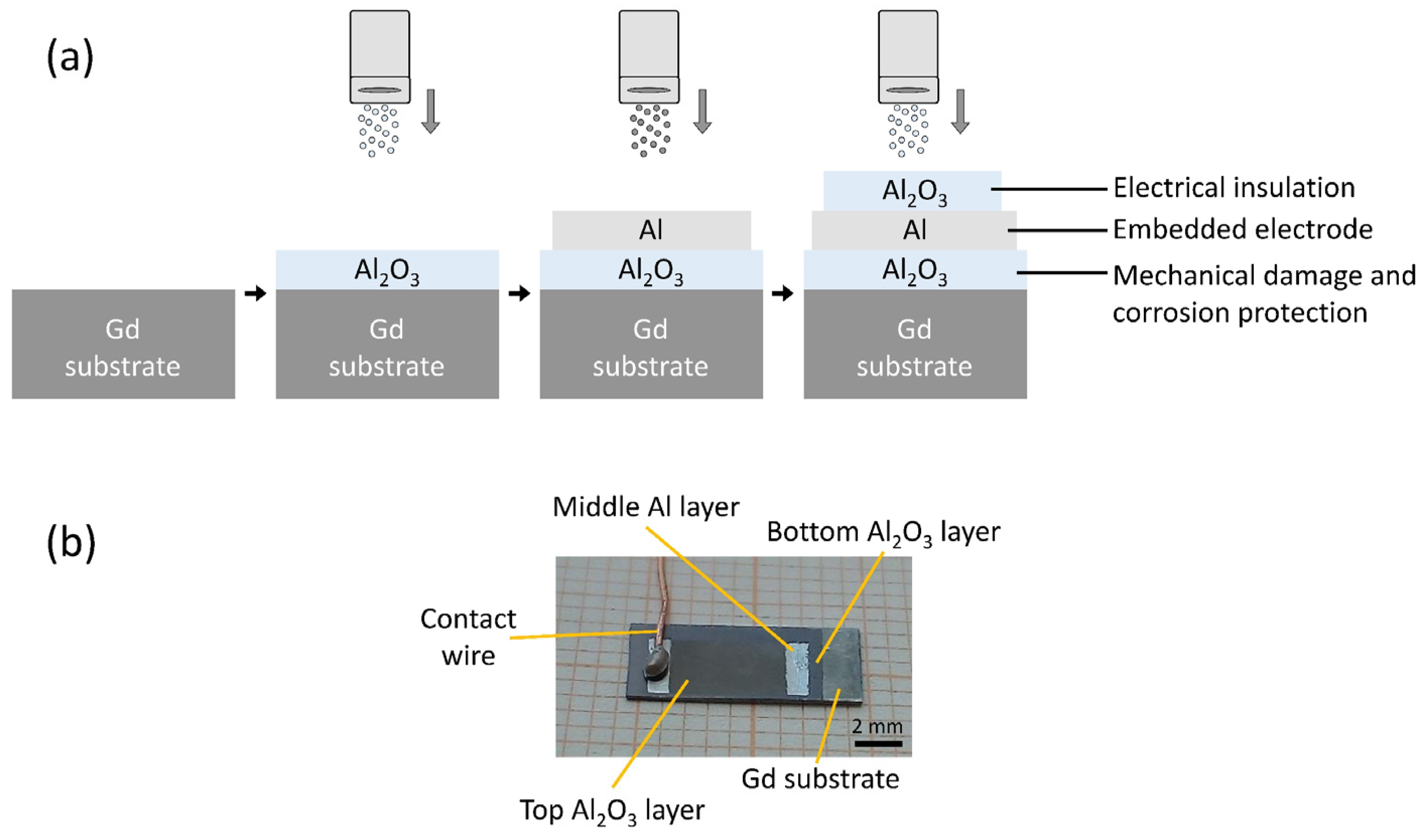
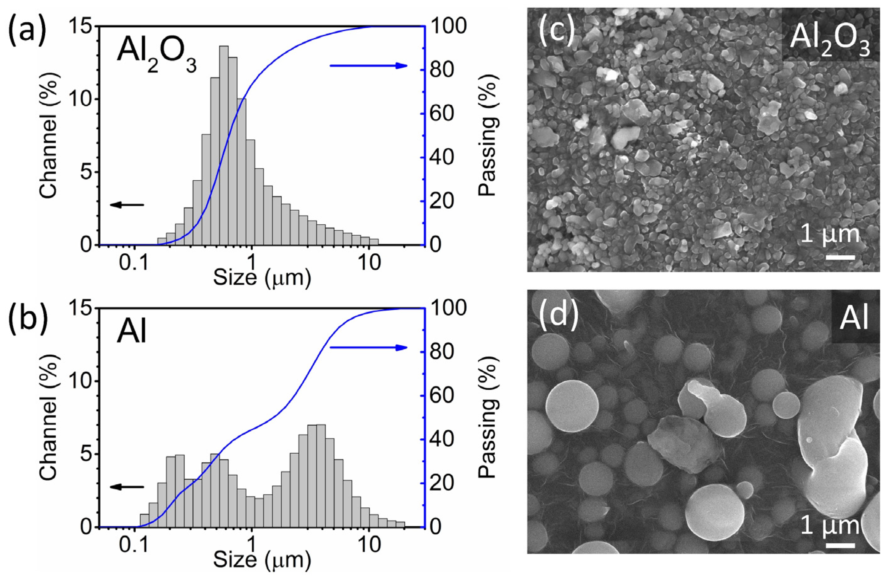
2. Materials and Methods
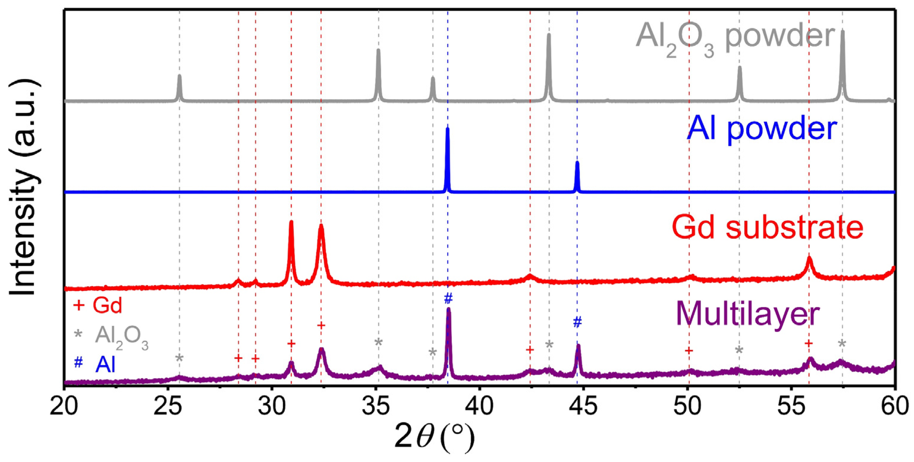
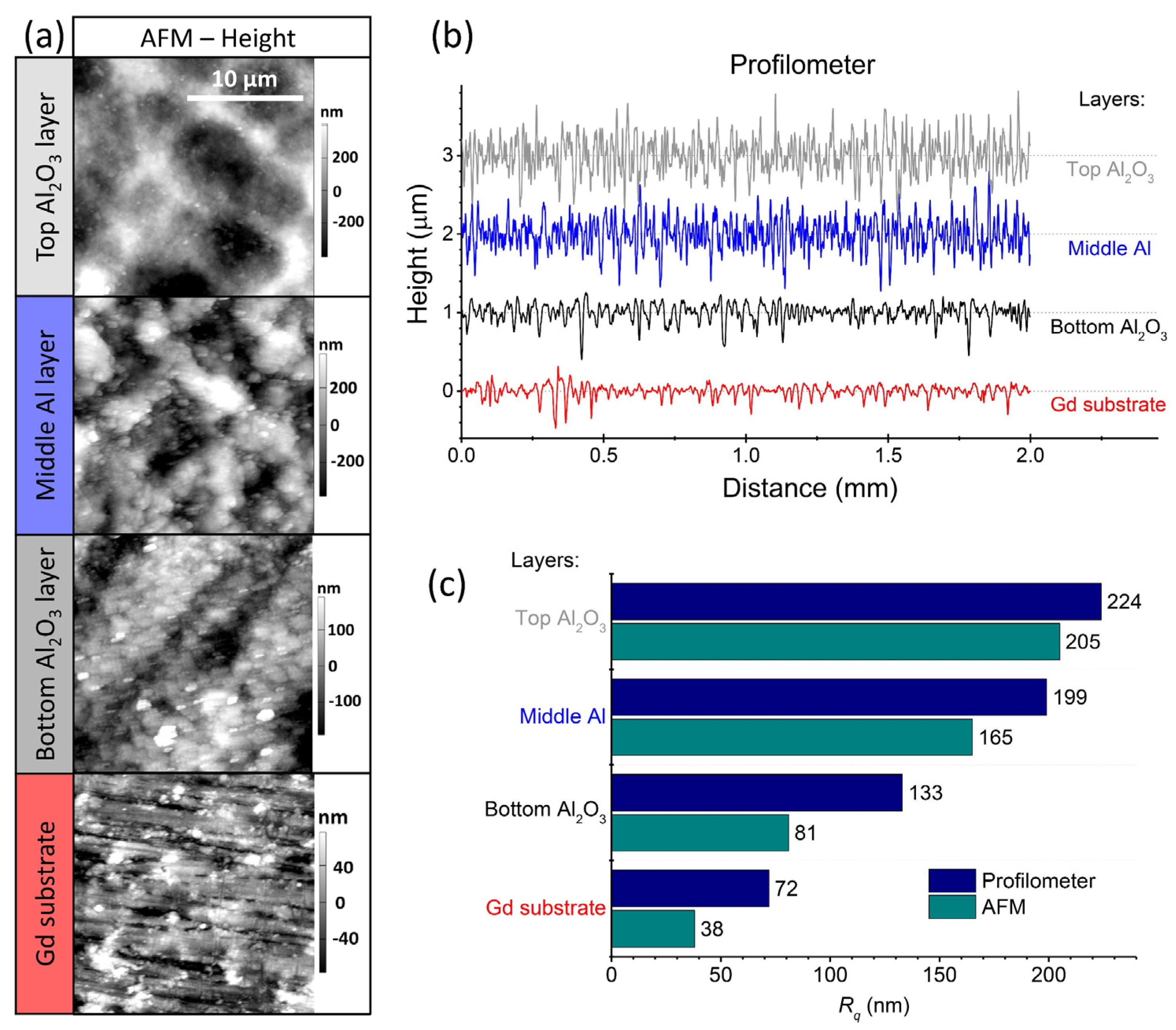
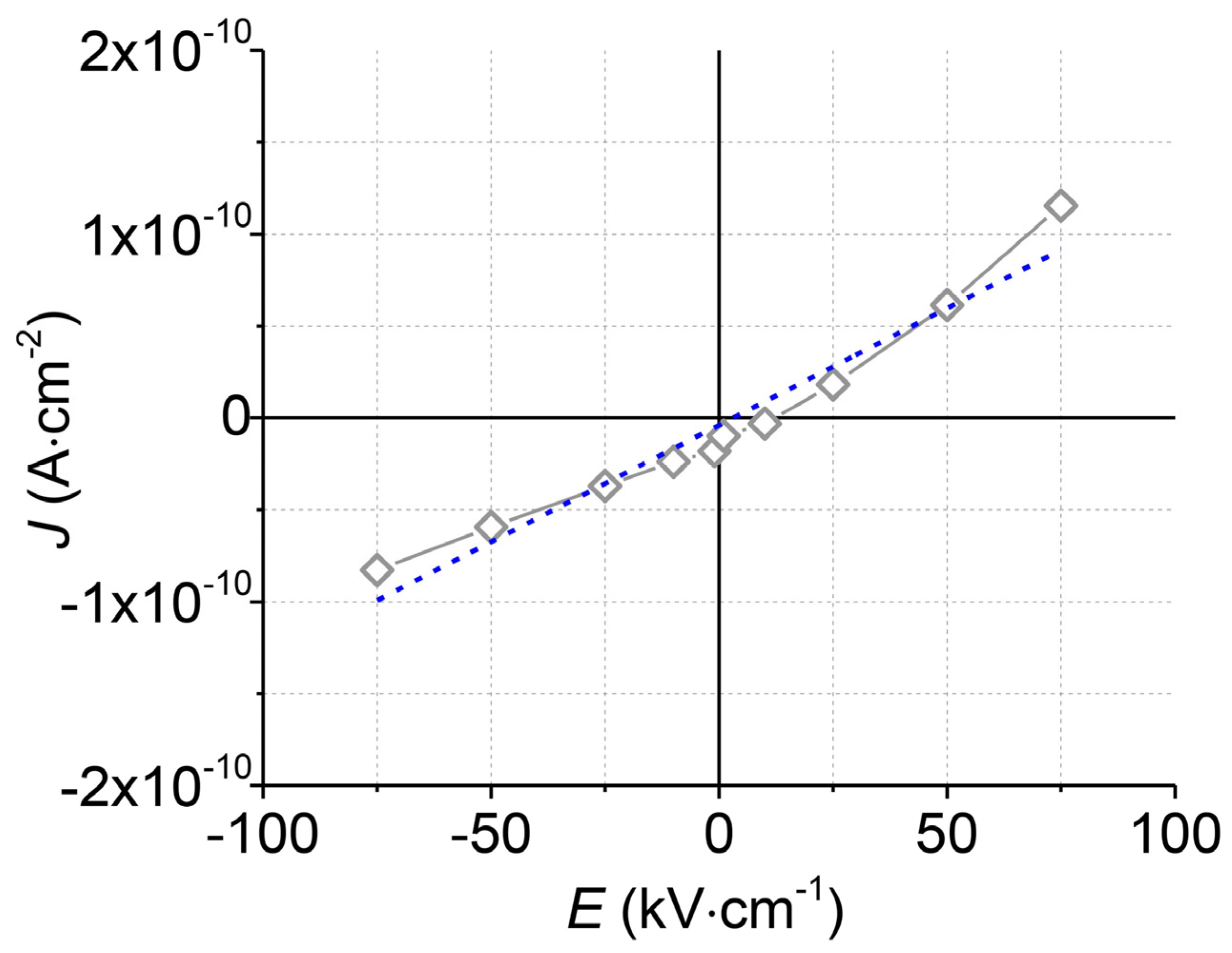
In the AD, a raw Al powder (99.96 %, 2 HPC, Toyal Europe, Accous, France) and an Al2O3 powder (99.8 %, A 16 SG, Almatis, Ludwigshafen, Germany) were used. The Al2O3 powder was thermally treated in a chamber furnace (Custom-made, Terna, Ljubljana, Slovenia) at 1150 °C for 1 h (with 5 K∙min−1 heating and cooling rates) and additionally milled in a planetary ball mill (PM400, Retsch, Haan, Germany) at 200 min−1 for 5 h using Al2O3 milling jar and yttria-stabilised-zirconia milling balls with diameters of 3 mm in iso-propanol as a liquid medium. The thermal treatment and the subsequent ball milling of the Al2O3 powder are necessary to achieve suitable particle size distribution for efficient AD [25]. In the case of Al, the as-received powder already resulted in successful film deposition. Therefore, no further powder modification was required. Prior to the AD, both powders were sieved through an 80-micrometre mesh and vacuum dried for 12 h at 100 °C and at 10 mbar. The AD apparatus was provided by InVerTec e.V., Bayreuth, Germany. Commercial gadolinium foils (Metall Rare Earth Limited, Hong Kong) were used as the substrate material. The process parameters used during the AD are shown in Table 1. The number of scans was adjusted to achieve the desired film thickness.
Particle size analyses of the raw Al powder and treated Al2O3 powders were performed using a light-scattering laser granulometer (S3500, Microtrac, York, PA, USA) with isopropanol as the medium. Scanning electron microscopy (SEM) and energy dispersive spectroscopy (EDS) analyses were performed using a field-emission scanning electron microscope (FE-SEM, JSM-7600F, JEOL, Tokyo, Japan) equipped with an energy dispersive X-ray spectrometer (Inca Oxford 350 EDS SSD, Oxford Instruments, Abingdon, UK). For the SEM powder analyses, Al2O3 and Al powders were deposited on carbon tape. For the cross-sectional analysis of the multilayers, the samples were cut, mounted in epoxy resin, ground and fine-polished with a colloidal silica suspension. Prior to the SEM analyses, all the samples were coated with a 3-nanometre-thick carbon layer using a Precision Etching and Coating System (PECS 682, Gatan, Pleasanton, CA, USA).
The X-ray diffraction (XRD) analysis was performed using a high-resolution diffractometer (X’Pert PRO, PANalytical, Almelo, The Netherlands) with Cu–Kα1 radiation. Diffraction patterns were recorded in the BraggBrentano geometry with a 100-channel X’Celerator detector in a 2θ range 10–120° with a step of 0.017° and an integration time of 100 s per step. The software X’Pert HighScore Plus 2.1, PANalytical was used to analyse the XRD patterns and to estimate the penetration depth of X-rays in the multilayer samples during XRD analysis. In the case of the multilayer sample, the X-rays penetrate all deposited layers (top Al2O3 layer, middle Al layer and bottom Al2O3 layer) and reach the Gd substrate, since the penetration depth is higher than the thickness of deposited layers. The total thickness of deposited layers is ~8 µm; while the calculated penetration depth for Al and Al2O3 at 2θ of 10° is ~30 µm and the value even increases with increasing 2θ angle.
The Topas R package (version 2.1, Bruker AXS GmbH, Karlsruhe, Germany) was employed for the Rietveld refinement and the Fundamental Parameters Approach (FPA) was used for line-profile fitting of all samples [30]. The FPA uses the geometrical properties of the diffraction experiment to build up the instrumental linewidth from first principles. It, thus, allows an explicit determination of the sample-dependent, line-broadening contributions to the peak profile, which are dominated by the microstrain and the broadening of the crystallite size [31].
The topography of the layers was analysed using atomic force microscopy (AFM) and contact stylus profilometry. The 20-micrometre line scans were acquired using an atomic force microscope (Jupiter XR, Asylum Research, Santa Barbara, CA, USA) in AC air topography mode. A Si tip on a Si/Al cantilever with a diameter of ~7 nm (AC240TS-R3, Asylum Research, Santa Barbara, CA, USA) was used for scanning. A contact stylus profilometer (DektakXT, Bruker, Karlsruhe, Germany) was used to measure 2-millimetre line scans. Then, the root-mean-square surface roughness (Rq) was determined from the roughness profile obtained after high-pass filtering of the primary profile with a cut-off wavelength of 0.08 mm.
Silver electrodes with a diameter of 0.75 mm were deposited on the top Al2O3 layer before electrical characterisation. Current density–electric field (J–E) measurements were performed using a Keithley 237 high-voltage-source measurement unit (Keithley Instruments, Cleveland, OH, USA). A step-like electric field in the range ±75 kV∙cm−1 was applied between Al layer and silver electrodes. The electrical resistivity was determined from the slope of the J–E curve, assuming Ohm’s law.

3. Results

We prepared an Al2O3/Al/Al2O3 multilayer structure on the surface of a magnetocaloric gadolinium element. A schematic representation and a photograph of the multilayer structure are shown in Figure 1a,b, respectively. First, the Gd substrate was almost completely covered with an Al2O3 layer, followed by the deposition of an Al layer. Then, the Al2O3 layer was deposited on top of the Al layer, keeping certain areas free to allow for electrical connections (i.e., placement of the contact wires). The first Al2O3 layer protects the Gd substrate from the environment and prevents corrosion and mechanical damage. The second Al layer is an electrically conductive electrode layer covered by the third Al2O3 layer, which electrically insulates the Al surface and completes the multilayer structure with an embedded electrode.
The Al2O3 and Al powders used in the deposition were analysed using laser granulometry and SEM. Laser granulometry shows a monomodal (Figure 2a) and a multi-modal (Figure 2b) particle size distribution of the Al2O3 and Al powders, respectively. The particle size range of the two powders is between 0.1 and 20 µm, and the median particle size (d50) of the Al2O3 and Al powders is 0.6 and 1.5 µm, respectively. The most abundant particle size fraction of the Al2O3 powder is represented by the peak at 0.6 µm, while the Al powder contains three peaks at 0.2, 0.5 and 3 µm. Both powders have an acceptable particle size range for the AD. In the literature, particles with sizes between a few hundred nm and a few µm are generally considered suitable for deposition and produce dense thick films with good adhesion [4,6]. According to the SEM analysis, the Al powder exhibits round particles, often with a perfect circular shape (Figure 2d). In contrast, the Al2O3 particles are irregularly shaped with smooth edges (Figure 2c).
XRD analysis (Figure 3) was performed on the Al2O3 and Al powders, on the Gd substrate and on the multilayer sample after deposition. The XRD patterns of the Al2O3 and Al powders contained only Al2O3 (JCPDS 46-1212) and Al reflections (JCPDS 89-2769), respectively. Therefore, no significant powder contamination in the ball milling process of the Al2O3 powder was detected. The very sharp peaks indicate large crystallites (>100 nm) and no microstrain in both powders. As expected, the XRD pattern of the Gd substrate also exhibits sharp Gd reflections (JCPDS 89-2924) with no impurities. After deposition, the XRD pattern of the multilayer (purple) shows the reflections of the Al layer, the Al2O3 layer and the Gd substrate. None of the three phases underwent a phase transformation. In the multilayer, the Gd reflections (marked with a red cross) did not undergo any peak shift or change in the peak shape. Only the intensity of the Gd decreased, since the substrate was covered by Al2O3 and Al layers. After the deposition, the multilayer sample exhibits peak broadening of the Al2O3 (marked with a grey asterisk) and Al (marked with blue dash) reflections, indicating a decrease in the crystallite size and/or an increase in the microstrain due to the fragmentation of the colliding powder particles in the AD process [4,32]. To quantitatively evaluate the crystallite size and microstrain in the Al2O3 and Al deposited layers, we performed a Rietveld refinement. The calculated crystallite size and microstrain in the Al2O3 layers are 22 ± 4 nm and 0.46 ± 0.14%, respectively. On the other hand, the crystallites in the Al layers are larger, i.e., 98 ± 8 nm, while the microstrain is almost insignificant, i.e., 0.04 ± 0.01%. In conclusion, the XRD results show that the deposition of Al2O3 leads to a much larger decrease in crystallite size and an increase in microstrain compared to Al.
Previously, it was reported that a significant reduction in the crystallite size and an increase in the microstrain after the deposition of an oxide powder are necessary conditions for successful film deposition [33]. According to our XRD analysis, the same hypothesis can be valid for the AD of ceramic Al2O3, but not completely for the AD of metallic Al. Both Al2O3 and Al powders formed consolidated layers, but only the ceramic Al2O3 powder obtained significant peak broadening, indicating that the cracking and fragmentation of particles predominate in the deposition mechanism. On the other hand, the deposition mechanism of ductile metals is different from that of ceramics. The less intense XRD peak broadening of Al indicates that plastic deformation is more prevalent in the deposition mechanism of metals.
The SEM and EDS analyses of the multilayer structure in cross-section are shown in Figure 4. All the deposited layers are very dense without any visible pores (Figure 4a). The thickness of the deposited Al2O3, Al and Al2O3 layers (bottom-up) is 5.0, 1.7 and 1.6 µm, respectively. Apparently, the roughness of the interfaces increases with the number of increasing layers. However, a sufficient layer thickness ensures good connectivity of the deposited layers. The interface between the layers is well defined (enlarged SEM images in Figure 4b,c), indicating good adhesion without any reactions. An additional adhesion test revealed no peeling off or delamination of the deposited layers (Supplementary material: Figure S1). The EDS map scans (Figure 4d–f) of the multilayer show a typical elemental distribution of the layers, which confirms no reaction between the layers.
The surface roughness of the deposited layers including the Gd substrate was evaluated using AFM and contact profilometry. The AFM map scans and the contact-profilometry line scans are shown in Figure 5a,b, respectively. A comparison of the root-mean-square surface roughness (Rq) between the two measurement methods is shown in Figure 5c. As expected, the values obtained with AFM are lower than those obtained with contact profilometry due to the hundred-times-smaller scanned area (20-micrometre lines in the case of the AFM and 2-millimetre lines in the case of the contact profilometry). However, the same trend is observed for both methods. The Rq is lowest for the Gd substrate and increases with each deposited layer. The Rq of the top Al2O3 layer is about 200 nm.
To test the electrical insulation of the upper Al2O3 layer, measurements of the current density (J) versus the electric field (E) were performed (Figure 6). The upper Al2O3 layer withstands high electric fields (75 kV·cm−1) without an electrical breakdown. The calculated electrical resistivity at room temperature is very high (7.7 × 10¹² Ω·m) and corresponds to the resistivity of the commercially available Al2O3 ceramics for electrical insulation [34,35].

4. Conclusions

We used the AD method to prepare an Al2O3/Al/Al2O3 multilayer composite on a Gd substrate. The complete room-temperature processing of the AD enabled the integration of metallic and ceramic materials that are otherwise incompatible at high temperatures. Inexpensive commercial powders with appropriate micrometre-sized particles were used for the successful film deposition. The SEM analysis revealed a dense multilayer with a defect-free microstructure and good intra-layer connectivity. In addition, the top Al2O3 dielectric layer provides excellent electrical resistance, which is required for reliable electric field application. In summary, we have shown that the fabrication of ceramic–metal multilayers using AD is feasible and represents a simple, reliable and cost-effective approach to functionalise and protect existing substrates. For example, the deposited Al2O3/Al/Al2O3 multilayers on the Gd substrate provide an excellent starting point for the development of future electrowetting-on-dielectric devices.

Supplementary Materials

The following are available online at https://www.mdpi.com/article/10.3390/ma14164548/s1, Figure S1: Images of the sample surface (top Al2O3 layer) taken with an optical light microscope. (a) before and (b) after the adhesion test.

Author Contributions

Conceptualisation, M.S., U.T. and H.U.; methodology, M.S., U.T. and H.U.; investigation, M.S., U.T. and H.U.; resources, M.S. and U.T.; data curation, M.S. and H.U; writing—original draft preparation, M.S. and H.U; writing—review and editing, M.S., U.T. and H.U.; visualisation, M.S.; supervision, H.U. All authors have read and agreed to the published version of the manuscript.

Funding

This research was funded by Jožef Stefan Institute Director’s fund 2017-ULTRACOOL and the Slovenian Research Agency, project N2-0212, young researcher project PR-08977, post-doctoral project Digital microfluidics in magnetocalorics (Z2-9247) and research core funding P2-0105.

Data Availability Statement

The data presented in this study are available upon request from the corresponding author.

Acknowledgments

Technical support by J. Cilenšek and V. Fišinger is gratefully acknowledged.

Conflicts of Interest

The authors declare no conflict of interest.

References

  1. Kosec, M.; Kuscer, D.; Holc, J.; Pardo, L.; Ricote, J. Processing of Ferroelectric Ceramic Thick Films. In Multifunctional Polycrystalline Ferroelectric Materials; Springer: Dordrech, The Netherlands, 2011. [Google Scholar]
  2. Pan, M.-J.; Randall, C. A brief introduction to ceramic capacitors. IEEE Electr. Insul. Mag. 2010, 26, 44–50. [Google Scholar] [CrossRef]
  3. Schubert, M.; Hanft, D.; Nazarenus, T.; Exner, J.; Nieke, P.; Glosse, P.; Leupold, N.; Kita, J.; Moos, R. Powder aerosol deposition method—Novel applications in the field of sensing and energy technology. Funct. Mater. Lett. 2019, 12, 1930005. [Google Scholar] [CrossRef] [Green Version]
  4. Hanft, D.; Exner, J.; Schubert, M.; Stöcker, T.; Fuierer, P.; Moos, R. An overview of the Aerosol Deposition method: Process fundamentals and new trends in materials applications. J. Ceram. Sci. Technol. 2015, 6, 147–181. [Google Scholar] [CrossRef]
  5. Lee, D.-W.; Kim, H.-J.; Kim, Y.-H.; Yun, Y.-H.; Nam, S.-M. Growth Process of alpha-Al2O3 Ceramic Films on Metal Substrates Fabricated at Room Temperature by Aerosol Deposition. J. Am. Ceram. Soc. 2011, 94, 3131–3138. [Google Scholar] [CrossRef]
  6. Akedo, J. Room Temperature Impact Consolidation (RTIC) of Fine Ceramic Powder by Aerosol Deposition Method and Applications to Microdevices. J. Therm. Spray Technol. 2008, 17, 181–198. [Google Scholar] [CrossRef]
  7. Saunders, R.; Johnson, S.D.; Schwer, D.; Patterson, E.A.; Ryou, H.; Gorzkowski, E.P. A Self-Consistent Scheme for Understanding Particle Impact and Adhesion in the Aerosol Deposition Process. J. Therm. Spray Technol. 2021, 30, 523–541. [Google Scholar] [CrossRef]
  8. Ryu, J.; Park, D.-S.; Hahn, B.-D.; Choi, J.-J.; Yoon, W.-H.; Kim, K.-Y.; Yun, H.-S. Photocatalytic TiO2 thin films by aerosol-deposition: From micron-sized particles to nano-grained thin film at room temperature. Appl. Catal. B Environ. 2008, 83, 1–7. [Google Scholar] [CrossRef]
  9. Lee, B.-K.; Park, D.-S.; Yoon, W.-H.; Ryu, J.-H.; Hahn, B.-D.; Choi, J.-J. Microstructure and Properties of Yttria Film Prepared by Aerosol Deposition. J. Korean Ceram. Soc. 2009, 46, 441–446. [Google Scholar] [CrossRef] [Green Version]
  10. Baba, S.; Tsuda, H.; Akedo, J. Thickness dependence of electrical properties of PZT films deposited on metal substrates by laser-assisted aerosol deposition. IEEE Trans. Ultrason. Ferroelectr. Freq. Control 2008, 55, 1009–1016. [Google Scholar] [CrossRef]
  11. Khansur, N.H.; Eckstein, U.; Benker, L.; Deisinger, U.; Merle, B.; Webber, K.G. Room temperature deposition of functional ceramic films on low-cost metal substrate. Ceram. Int. 2018, 44, 16295–16301. [Google Scholar] [CrossRef]
  12. Heo, Y.J.; Kim, H.T.; Kim, K.J.; Nahm, S.; Yoon, Y.J.; Kim, J. Enhanced heat transfer by room temperature deposition of AlN film on aluminum for a light emitting diode package. Appl. Therm. Eng. 2013, 50, 799–804. [Google Scholar] [CrossRef]
  13. Park, D.-S.; Kim, I.-S.; Kim, H.; Chou, A.H.K.; Hahn, B.-D.; Li, L.-H.; Hwang, S.-J. Improved biocompatibility of hydroxyapatite thin film prepared by aerosol deposition. J. Biomed. Mater. Res. Part B Appl. Biomater. 2010, 94, 353–358. [Google Scholar] [CrossRef]
  14. Papyrin, A. Cold Spray Technology. Adv. Mater. Proc. 2001, 159, 49–51. [Google Scholar]
  15. Kim, Y.-H.; Lee, J.-W.; Kim, H.-J.; Yun, Y.-H.; Nam, S.-M. Silver metallization for microwave device using aerosol deposition. Ceram. Int. 2012, 38, S201–S204. [Google Scholar] [CrossRef]
  16. Lee, D.-W.; Kwon, O.-Y.; Cho, W.-J.; Song, J.-K.; Kim, Y.-N. Characteristics and Mechanism of Cu Films Fabricated at Room Temperature by Aerosol Deposition. Nanoscale Res. Lett. 2016, 11, 1–8. [Google Scholar] [CrossRef] [PubMed] [Green Version]
  17. Khansur, N.H.; Eckstein, U.; Ursic, H.; Sadl, M.; Brehl, M.; Martin, A.; Riess, K.; de Ligny, D.; Webber, K.G. Enhanced Electromechanical Response and Thermal Stability of 0.93(Na1/2Bi1/2)TiO3-0.07BaTiO3 Through Aerosol Deposition of Base Metal Electrodes. Adv. Mater. Interfaces 2021, 8, 2100309. [Google Scholar] [CrossRef]
  18. Cho, M.-Y.; Lee, D.-W.; Kim, I.-S.; Lee, W.-H.; Yoo, J.-W.; Ko, P.-J.; Koo, S.-M.; Choi, Y.-K.; Oh, J.-M. Formation of silver films for advanced electrical properties by using aerosol deposition process. Jpn. J. Appl. Phys. 2018, 57, 11UF05. [Google Scholar] [CrossRef]
  19. Leupold, N.; Denneler, S.; Rieger, G.; Moos, R. Powder Treatment for Increased Thickness of Iron Coatings Produced by the Powder Aerosol Deposition Method and Formation of Iron–Alumina Multilayer Structures. J. Therm. Spray Technol. 2020, 30, 480–487. [Google Scholar] [CrossRef]
  20. Sugimoto, S.; Chan, V.; Noguchi, M.; Tezuka, N.; Inomata, K.; Akedo, J. Preparation of Fe/Ni–Zn–Cu ferrite stacked films by aerosol deposition method. J. Magn. Magn. Mater. 2007, 310, 2549–2551. [Google Scholar] [CrossRef]
  21. Kwon, J.; Park, H.; Lee, I.; Lee, C. Effect of gas flow rate on deposition behavior of Fe-based amorphous alloys in vacuum kinetic spray process. Surf. Coat. Technol. 2014, 259, 585–593. [Google Scholar] [CrossRef]
  22. Imanaka, Y.; Akedo, J. Embedded capacitor technology using aerosol deposition. Int. J. Appl. Ceram. Technol. 2010, 7, 23–32. [Google Scholar] [CrossRef]
  23. Miyoshi, T. Preparation of multilayer piezoelectric device by aerosol deposition using a novel detachment method. J. Ceram. Soc. Jpn. 2009, 117, 899–903. [Google Scholar] [CrossRef] [Green Version]
  24. Kambale, R.C.; Han, G.; Yoon, W.-H.; Kim, J.-W.; Choi, J.-J.; Hahn, B.-D.; Park, D.-S.; Ahn, C.-W.; Ryu, J. Reliability of ferroelectric multilayer PZT thick films fabricated by aerosol deposition. Ferroelectrics 2014, 470, 183–193. [Google Scholar] [CrossRef]
  25. Sadl, M.; Tomc, U.; Prah, U.; Ursic, H. Protective Alumina Coatings Prepared by Aerosol Deposition on Magnetocaloric Gadolinium Elements. Inf. MIDEM J. Microelectron. Electron. Compon. Mater. 2019, 49, 177–182. [Google Scholar] [CrossRef]
  26. Cha, G.; Kim, C.-J.; Ju, Y.S. Thermal conductance switching based on the actuation of liquid droplets through the electrowetting on dielectric (EWOD) phenomenon. Appl. Therm. Eng. 2016, 98, 189–195. [Google Scholar] [CrossRef] [Green Version]
  27. Klinar, K.; Kitanovski, A. Thermal control elements for caloric energy conversion. In Renewable and Sustainable Energy Reviews; Elsevier: Amsterdam, The Netherlands, 2020; Volume 118, p. 109571. [Google Scholar] [CrossRef]
  28. Swoboda, T.; Klinar, K.; Yalamarthy, A.S.; Kitanovski, A.; Rojo, M.M. Solid-State Thermal Control Devices. In Advanced Electronic Materials; Blackwell Publishing Ltd.: Hoboken, NJ, USA, 2021; Volume 7, p. 2000625. [Google Scholar] [CrossRef]
  29. Klinar, K.; Swoboda, T.; Rojo, M.M.; Kitanovski, A. Fluidic and Mechanical Thermal Control Devices. In Advanced Electronic Materials; Blackwell Publishing Ltd.: Hoboken, NJ, USA, 2021; Volume 7, p. 2000623. [Google Scholar] [CrossRef]
  30. Cheary, R.W.; Coelho, A. A fundamental parameters approach to X-ray line-profile fitting. J. Appl. Crystallogr. 1992, 25, 109–121. [Google Scholar] [CrossRef]
  31. Klug, H.P.; Alexander, L.E. X-Ray Diffraction Procedures: For Polycrystalline and Amorphous Materials, 2nd ed.; John Wiley & Sons: New York, NY, USA, 1974. [Google Scholar]
  32. Akedo, J. Aerosol deposition of ceramic thick films at room temperature: Densification mechanism of ceramic layers. J. Am. Ceram. Soc. 2006, 89, 1834–1839. [Google Scholar] [CrossRef]
  33. Exner, J.; Schubert, M.; Hanft, D.; Kita, J.; Moos, R. How to treat powders for the room temperature aerosol deposition method to avoid porous, low strength ceramic films. J. Eur. Ceram. Soc. 2019, 39, 592–600. [Google Scholar] [CrossRef]
  34. Barsoum, M.W. Fundamentals of Ceramics; CRC Press: Boca Raton, FL, USA, 2019. [Google Scholar]
  35. Kingery, W.D.; Bowen, H.K.; Uhlmann, D.R. Introduction to Ceramics; Wiley: London, UK, 1976. [Google Scholar]
Figure 1. (a) Schematic representation of the deposition process in the multilayer fabrication. (b) A photograph of the multi-layered structure with an electrical contact.
Materials 14 04548 g001
Figure 2. (a,b) Particle size distributions (grey) and cumulative curves (blue) determined using the laser granulometry and (c,d) scanning electron microscopy (SEM) images of Al2O3 and Al powders.
Materials 14 04548 g002
Figure 3. X-ray diffraction (XRD) patterns of the Al2O3 powder (grey), Al powder (blue), Gd substrate (red) and prepared multilayer sample (purple).
Materials 14 04548 g003
Figure 4. (a) Scanning electron microscopy (SEM) analysis of the multilayer structure in cross-section. Panels (b,c) show the magnified areas marked in (a). Energy dispersive spectroscopy (EDS) elemental mapping images are showing the distribution of (d) Al, (e) Gd and (f) O.
Materials 14 04548 g004
Figure 5. (a) Atomic force microscopy (AFM) map scans and (b) contact-profilometer line scans of the deposited layers, including the Gd substrate. The corresponding Rq values of the two methods, AFM (cyan) and contact profilometry (dark blue), are shown in (c).
Materials 14 04548 g005
Figure 6. The current density (J) vs. electric field (E) curve (grey) of the top Al2O3 layer and its linear approximation (blue).
Materials 14 04548 g006
Table 1. Process parameters used during the AD.
Process ParametersAl2O3 PowderAl Powder
Carrier gas speciesN2
Nozzle geometry (slit size)(0.5 × 10) mm2
Distance between nozzle and substrate5 mm
Sweep speed5 mm·s−1
Gas flow rate4 L·min−12 L·min−1
Pressure in aerosol chamber180 mbar120 mbar
Pressure in deposition chamber2 mbar1 mbar
Publisher’s Note: MDPI stays neutral with regard to jurisdictional claims in published maps and institutional affiliations.

