Article

Properties of Metallic and Oxide Thin Films Based on Ti and Co Prepared by Magnetron Sputtering from Sintered Targets with Different Co-Content

1
Faculty of Microsystem Electronics and Photonics, Wroclaw University of Science and Technology, Janiszewskiego 11/17, 50-372 Wroclaw, Poland
2
Lukasiewicz Research Network—Institute of Non-Ferrous Metals, Gliwice Division, Sowinskiego 5, 44-100 Gliwice, Poland
*
Author to whom correspondence should be addressed.
Materials 2021, 14(14), 3797; https://doi.org/10.3390/ma14143797
Submission received: 1 May 2021 / Revised: 14 June 2021 / Accepted: 5 July 2021 / Published: 7 July 2021
(This article belongs to the Special Issue The 44th IMAPS Poland Conference)

Abstract

:
In this work, selected properties of metallic and oxide thin films based on titanium and cobalt were described. Thin-film coatings were prepared using the magnetron sputtering method. The deposition was carried out from sintered targets with different Co-content (2 at.%, 12 at.% and 50 at.%). The relation between the Ti–Co target composition and the Co-content in the metallic and oxide films was examined. There was 15–20% more cobalt in the films than in the target. Moreover, the deposition rate under neutral conditions (in Ar plasma) was even 10-times higher compared to oxidizing Ar:O2 (70:30) plasma. A comprehensive analysis of the structural properties (performed with GIXRD and SEM) revealed the amorphous nature of (Ti,Co)Ox coatings, regardless of the cobalt content in the coating. The fine-grained, homogenous microstructure was observed, where cracks and voids were identified only for films with high Co-content. Optical studies have shown that these films were well transparent (60% ÷ 80%), and the amount of cobalt in the target from which they were sputtered had a significant impact on the decrease in the transparency level, the slight shift of the absorption edge position (from 279 nm to 289 nm) as well as the decrease in their optical band gap energy (from 3.13 eV to 1.71 eV). Electrical studies have shown that in (Ti,Co)Ox thin films, a unipolar memristive-like effect can be observed. The occurrence of such effects has not been reported so far in the case of TiO2 coatings with the addition of Co.

1. Introduction

The progress in electronic components functionality is related to the development of, among others, a new type of multifunctional thin-film coatings that will combine the features and attributes of various materials. Among the materials currently used in optoelectronics, titanium dioxide is well recognized whose production technology is mastered and has a wide application area. It is a very good matrix due to high chemical, thermal and mechanical resistance. This wide band gap oxide (ca. 3 eV) is neutral to the environment and exhibits high transparency for light in a wide spectral range (320 nm–6000 nm), has a high refractive index (2.4–2.7), and exhibits high photocatalytic activity [1,2]. TiO2 is used in the construction of optical filters [3], in solar cells [4] and as an active layer in gas sensors [5]. The properties of such transition metal oxides as TiO2 can be modified by a proper selection of deposition parameters, post-process treatment (e.g., annealing) or doping. Many additives and admixtures are used to modify the properties of TiO2. Cobalt can also be included, but its influence on the properties of titanium dioxide is not yet well understood. There are no comprehensive studies on thin films based on titanium and cobalt (especially in the form of oxides) that limit the possibility of fully exploiting the potential that the combination of these two materials can offer. Cobalt and its oxides exhibit high stability (especially in the form of CoO and Co3O4) [6], as well as high photocatalytic activity [7] or ferromagnetic properties [8]. Oxides and metallic materials based on Co can be applied in spintronics [9], magneto-optical devices [10], in the construction of semiconductor sensors [11], electrochromic coatings [12] and heterogeneous catalysts [13]. Materials based on titanium and cobalt constitute a “new group” of materials whose properties have not been fully understood and used so far. Doping titanium dioxide with cobalt allows to modify a number of its properties, primarily: structural [14,15,16,17,18,19,20,21], optical [14,15,16,17,18,20,21], electrical [15,16,20,21] and magnetic [20]. These coatings have been of great interest due to the formation of dilute magnetic semiconductors (DMS), which is promising for the manufacturing of spintronic and magneto-optic devices [22,23,24]. Co-doped TiO2 is a ferromagnetic material at room temperature [25] that turns it into a promising material for magneto-resistive random-access memory (MRAM) [24].
The properties of doped coatings based on titanium and its oxides largely depend on the method of their preparation. Among the many methods and their use in the electronics industry, attention should be paid to magnetron sputtering. It requires the use of targets that are the source of the sputtered material over which the plasma is ignited. Unfortunately, due to the magnetic properties of cobalt, it closes the magnetic field, and it is difficult to ignite the plasma over a magnetron with such a target. A solution can be the use of thin Co targets or multicomponent targets such as Ti–Co. This paper presents studies of the structural, optical and electrical properties of thin (Ti,Co)Ox coatings. They were obtained by magnetron sputtering, and the analysis of their properties was described from the stage of sintering Ti–Co targets (with different material compositions) using the SPS method. It was necessary to determine the relationship between the cobalt content in the target and its final amount in both the metallic and oxide films. The results of electrical measurements have shown that in (Ti,Co)Ox thin films, a unipolar memristive-like effect can be observed. The occurrence of such effects has not been reported so far in the case of TiO2 coatings with the addition of Co. This means that materials based on titanium and cobalt oxides may be prospective for electronics, not only due to their well-known spintronic properties but also because of their memristive-like behavior.

2. Experimental

2.1. Preparation of Targets and Thin Films

Metallic and oxide thin films were prepared using the magnetron sputtering method. For the preparation, the Ti–Co targets with 2 at.%, 12 at.% and 50 at.% of Co-content were used. The targets were prepared by spark plasma sintering method (SPS) with the aid of the system provided by the FCT GmbH company [26,27]. Targets were sintered at 1200 °C in a graphite matrix. They had a diameter of 30 mm and a thickness of 3 mm. The material composition of the targets was determined by a JXA-8230 X-ray microanalyzer (JEOL) with wave and energy dispersion spectrometers (WDS and EDS). These targets were used for the preparation of metallic and oxide thin films (Ti–Co and (Ti,Co)Ox, respectively). Pre-cleaning of the surface of targets and substrates was applied (low-pressure plasma discharge in the chamber: AC supply, 170 W, 1.2 × 10⁻¹ mbar, 3 min). Deposition processes were carried out using either pure Ar or a mixture of Ar:O2 (70:30) as a working and reactive gas. The constant gas flow was set during the entire deposition process at 26 sccm that was controlled by the ERG1MPSc unit (BetaERG). Films, as deposited in the argon atmosphere, were metallic, while the addition of 30% of oxygen was sufficient to obtain the full oxidation of the coatings. The pressure in a vacuum chamber during the process was 1.5 × 10⁻² mbar. The magnetron was powered by an MSS2 (2 kW) pulsed DC power supply unit (DORA Power System). The deposition process lasted 60 min for metallic and 120 min for oxide thin films. The substrates were placed on a rotating drum at a 100 mm distance from the sputtered target. Sputtering rate (SR) was calculated taking into consideration the film thickness and the time of material deposition on the given substrate holder area, which is sputtering time divided into 6. Films were deposited on fused silica (SiO2) and silicon wafers.

2.2. Methods of Targets and Thin Film Characterization

The thickness and surface topography of as-deposited thin films was determined by the optical profiler Talysurf CCI (Taylor Hobson, Leicester, UK). Based on three-dimensional profiles, the analysis of surface roughness was performed, and the value of root mean square roughness (Sq) was determined.
Surface observation and material composition of the metallic coatings was determined by a JXA-8230 (JEOL) X-ray microanalyzer equipped with WDS and EDS spectrometers. In the case of oxide (Ti,Co)Ox films, the observations of surface and cross-section morphology were performed with the use of FEI Helios NanoLab 600i SEM coupled with an EDS spectrometer. Comparison of the intensity of CoKα and TiKα emission lines allowed to determine the amount of each element.
The structure of the oxide coatings was determined using X-ray diffraction in grazing incidence mode (GIXRD) with the aid of Empyrean PIXel3D (Panalytical, Malvern, UK) diffractometer with Cu Kα radiation (0.15406 nm). The X-ray source was powered with 40 kV and 30 mA. The diffraction patterns were collected with the step size equal to 0.05° in the 2theta range of 20°–80° and time per step equal to 2 s. The incidence angle was constant and equal to 3° to the sample surface. For data analysis, MDI JADE 5.0 software (ICDD, Newtown Square, PA, USA) was used.
The optical properties of oxide coatings were analyzed based on transmission characteristics. Measurements were conducted in the wavelength range of 250–900 nm using Ocean Optics QE65000 spectrophotometer (Ocean Optics, Largo, FL, USA) and a coupled deuterium-halogen light source. The analysis carried out based on the obtained data allowed to determine the cut-off wavelength (λcut-off) and optical band gap energy (Egopt).
Electrical properties were determined based on the DC current-to-voltage electrical measurements using a Keithley SCS4200 semiconductor characterization system (Keithley Instruments LLC, Cleveland, OH, USA) and an M100 probe station (Cascade Microtech, Beaverton, OR, USA). The setup for the measurement of the capacitance–voltage characteristics was also additionally equipped with an Agilent 4294A precision impedance analyzer (Agilent Technologies Inc., Santa Clara, CA, USA) To allow electrical tests, circular gold 1 mm pads were evaporated at the top of the (Ti,Co)Ox thin film deposited on the silicon substrate. Measurements of C–V characteristics were performed for 100 equally repeated cycles.

3. Results and Discussion

Thin-film coatings based on Ti and Co can have a wide application area in electronic and optoelectronic devices. As mentioned, especially transparent oxide coatings based on Ti–Co oxides can be used in many different areas. However, defining their properties (currently very poorly understood and described in the literature) requires reproducible mass-scale manufacturing, which can be provided by, e.g., magnetron sputtering. In this paper, first, the influence of the working gas atmosphere (neutral—Ar and oxidizing Ar:O2) in which Ti–Co targets were sputtered on the properties of the prepared coatings is discussed. The effect of Co-content in the target on the deposition rate was investigated. The next part is devoted to the analysis of a very broad characterization of the structural, optical and electrical properties of oxide (Ti,Co)Ox coatings in relation to their potential areas of application in electronics and optoelectronics.

3.1. Influence of Ti–Co Target Composition on Its Sputtering Conditions

3.1.1. Material Composition of Sintered Ti–Co Targets

In Figure 1, the microstructure with a WDS-map of the elemental distribution of the targets is shown. It was found that the Co-content in the three prepared targets was ca. 2 at.%, 12 at.% and 50 at.% (the exact numbers are collected in Table 1). The distribution of the elements in the Ti0.98Co0.02 target indicates that cobalt is dissolved in titanium in the entire volume of the target (Figure 1a). Cobalt content in the Ti0.98Co0.02 target is slightly different from the assumed one (1.7 at.%). This may be related due to the accuracy of the method or the effect of material segregation in the volume of the entire target. In the case of the Ti0.88Co0.12 target, high segregation of elements can be macroscopically observed. In the center of the Ti0.88Co0.12 target, the presence of a bright area of the Ti–Co phase and black ones of titanium are observed—most probably due to low cobalt dissolution (Figure 1b). The results of the WDS analysis of the Ti0.50Co0.50 target suggest a finely divided structure with visible dark areas which are richer in titanium (Figure 1c).

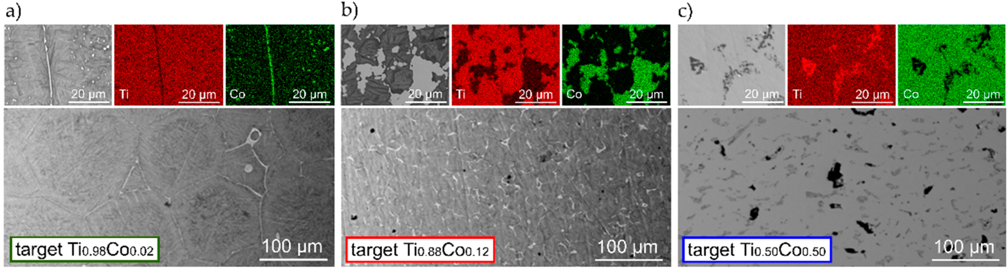
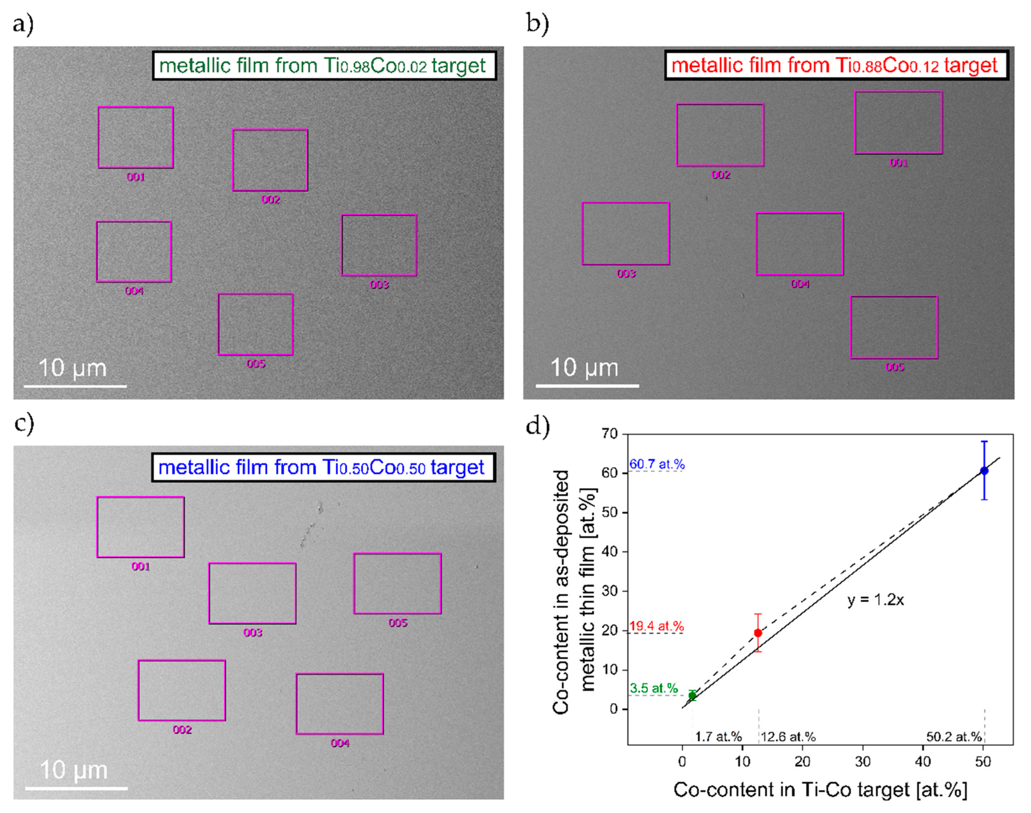
3.1.2. Material Composition of Metallic Ti–Co Thin Films

In Figure 2, images of surface topography with marked areas of EDS analysis for metallic Ti–Co thin films as deposited from Ti0.98Co0.02, Ti0.88Co0.12 and Ti0.50Co0.50 targets are shown.
Based on these results, a diagram of the relation between Co-content in the target and in the metallic film is shown in Figure 2d. The EDS results (obtained for five randomly selected areas on each sample) showed that the distribution of cobalt in the metallic films was homogeneous. It was also found that the Co-amount in the films was relatively 20% higher than in the targets. Detailed results of the material composition research of metallic coatings are summarized in Table 1.

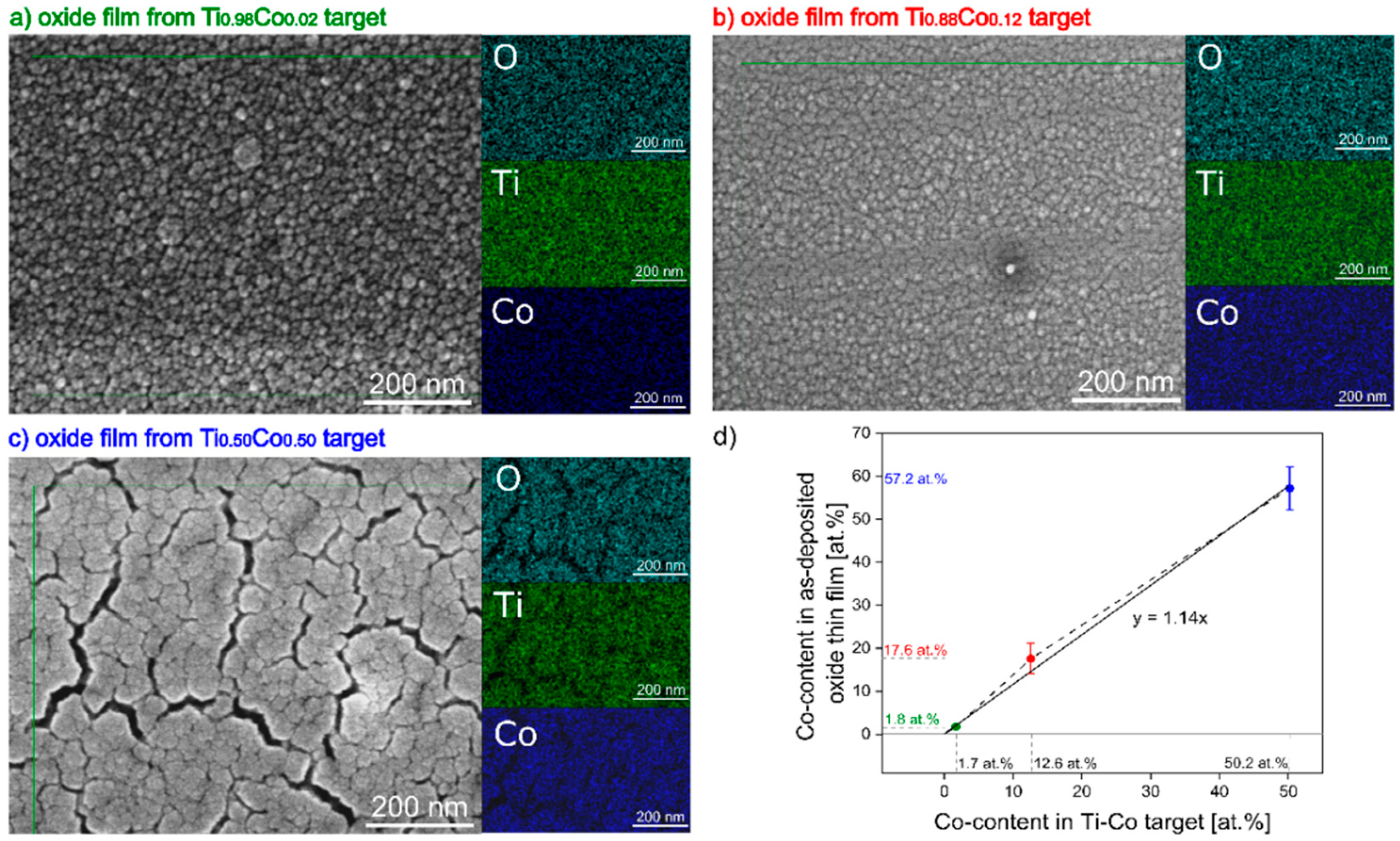
3.1.3. Material Composition of Oxide (Ti,Co)Ox Thin Films

In Figure 3, the SEM images of surface topography with EDS maps of elemental distribution for oxide (Ti,Co)Ox thin films as deposited from Ti0.98Co0.02, Ti0.88Co0.12 and Ti0.50Co0.50 targets are shown. These results were used to draw up a diagram (Figure 3d) showing the relationship between the composition of the target and the oxide film. EDS maps of Ti, O and Co indicate a homogeneous distribution of these elements and a lack of agglomeration effects. The absence of areas with a clearly higher concentration of titanium or cobalt is important. This proves the good quality of sintered targets and the possibility of manufacturing coatings with a homogeneous composition based on them. Moreover, it was found that in the oxide films, there was more Co compared to its content in the target. The factor of 1.15 can be used to estimate the cobalt content of oxide coatings made from sintered Ti–Co targets. The 50 at.% amount of cobalt also causes stresses in the structure, which results in the presence of nano cracks in the microstructure of the (Ti,Co)Ox film (Figure 3c). Detailed results of EDS analysis are collected in Table 1.
The relationship between the composition of Ti–Co targets and the content of cobalt in as-deposited metallic and oxide films can also be analyzed based on the detailed data, which are collected in Table 1. As can be seen, there was relatively 15% ÷ 20% more cobalt in the films. These differences result from the sputtering yield of Co and Ti. In the case of oxide and metallic coatings deposited from the Ti0.88Co0.12 target, these differences are the greatest. However, it can be assumed that they result rather from the segregation of the titanium and cobalt atoms that were obtained with this target composition (see Figure 1b).

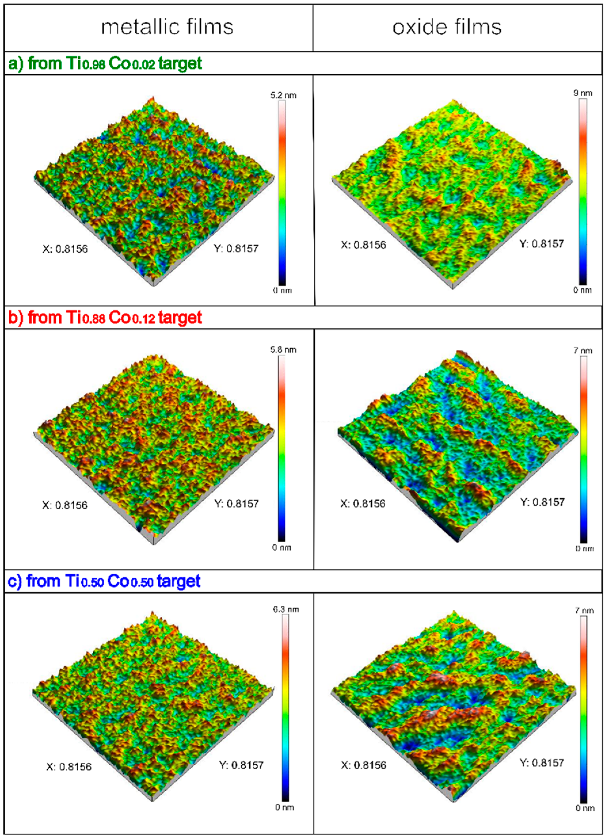
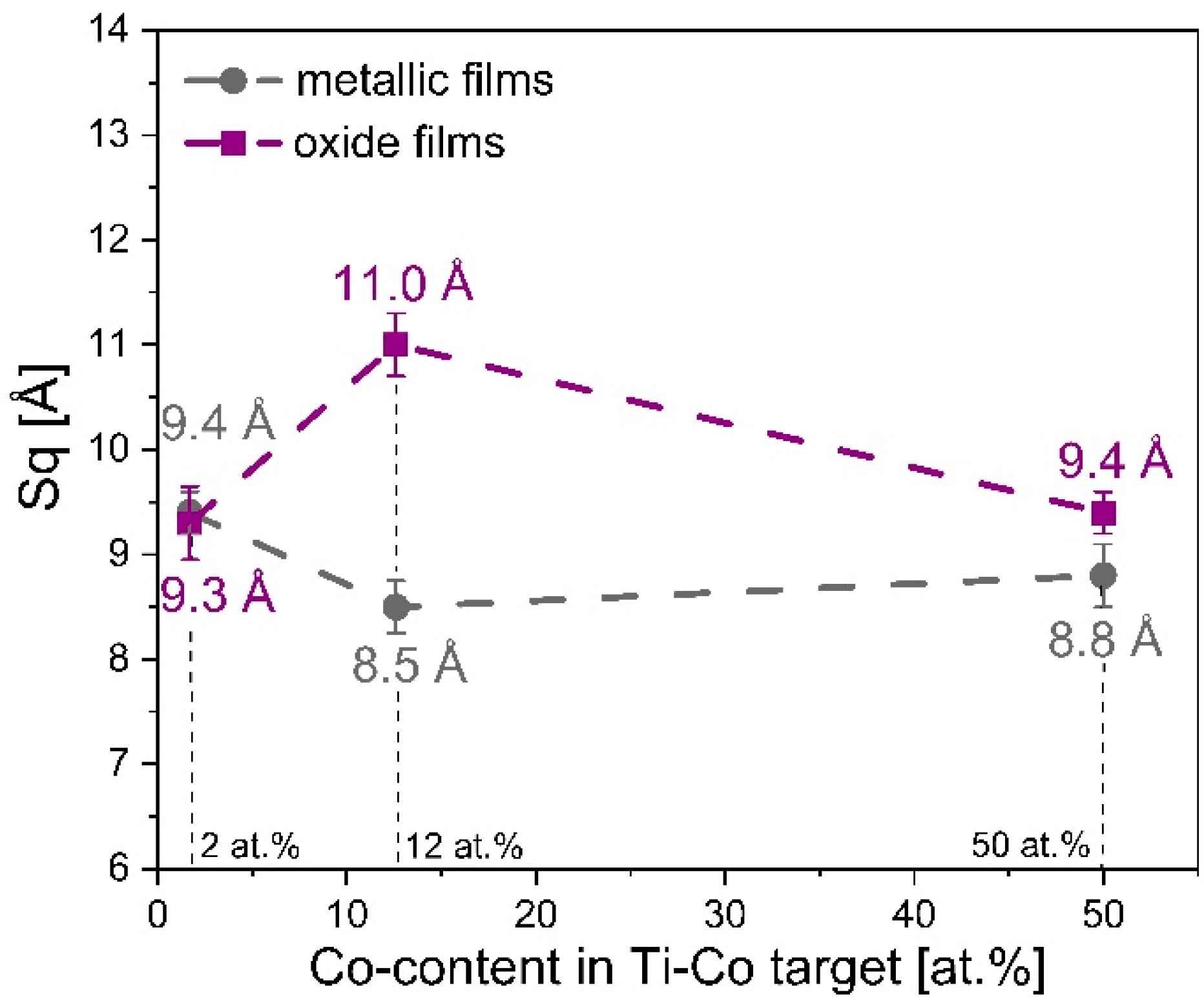
3.1.4. Roughness of Metallic Ti–Co and Oxide (Ti,Co)Ox Thin Films

The influence of target composition on its sputtering rate under argon—as an inert atmosphere as well as in Ar:O2 gas mixture (with 30% of oxygen)—as an oxidizing atmosphere was also studied with the aid of an optical profilometer. Figure 4 shows the three-dimensional surface profiles of metallic Ti–Co and oxide (Ti,Co)Ox coatings. As it can be seen, all prepared films were smooth and homogenous. A detailed analysis, based on the Sq parameter (the root mean square height of the surface), showed that the roughness was at the level of 1 nm ± 0.2 nm (Figure 5). However, metallic films are characterized by almost the same Sq value (0.9 nm), which can also be concluded based on their 3D profiles (almost identical). In the case of oxide (Ti,Co)Ox films, the values of Sq parameter are also very similar, although slight differences in surface topography can be observed on the 3D profiles.

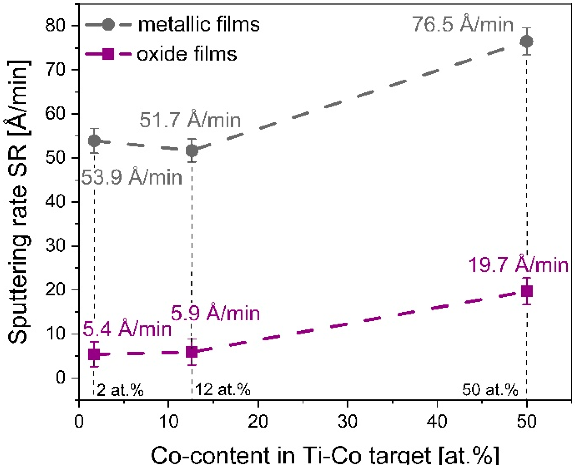
3.1.5. Sputtering Rate of T-Co Targets for Metallic and Oxide Films

Besides the roughness analysis, optical profilometry was also used for the determination of the film thickness. In the case of metallic Ti–Co films, the thickness was 324 nm, 310 nm and 460 nm (for 60 min of sputtering) for Ti0.98Co0.02, Ti0.88Co0.12 and Ti0.50Co0.50, respectively. The thickness of the oxide (Ti,Co)Ox films was 65 nm, 70 nm and 236 nm (for 120 min of sputtering), respectively. These results were in good agreement with SEM cross-section observations. Taking into account the deposition time of each coating and the construction of the substrate holder (drum with six sides), the sputtering rate was determined (Figure 6).
A common conclusion for all coatings is the fact that an increase in the amount of cobalt in the target causes an increase in its sputtering rate and thus the deposition rate of both metallic and oxide coatings. In the case of the Ti0.98Co0.02 and Ti0.88Co0.12 targets, the SR values are about 10-times higher in the argon itself than in the argon-oxygen gas mixture and are around 5 Å/min and 50 Å/min, respectively. For a higher cobalt content of the target, i.e., 50 at.%, the sputtering rate was approximately 20 Å/min and 75 Å/min in the Ar and Ar:O2 atmosphere, respectively. This proves that the use of an oxidizing atmosphere most likely causes the target poisoning effect and reduces its sputtering efficiency [28,29,30].

3.2. Structural, Optical and Electrical Characterization of (Ti,Co)Ox Thin Films

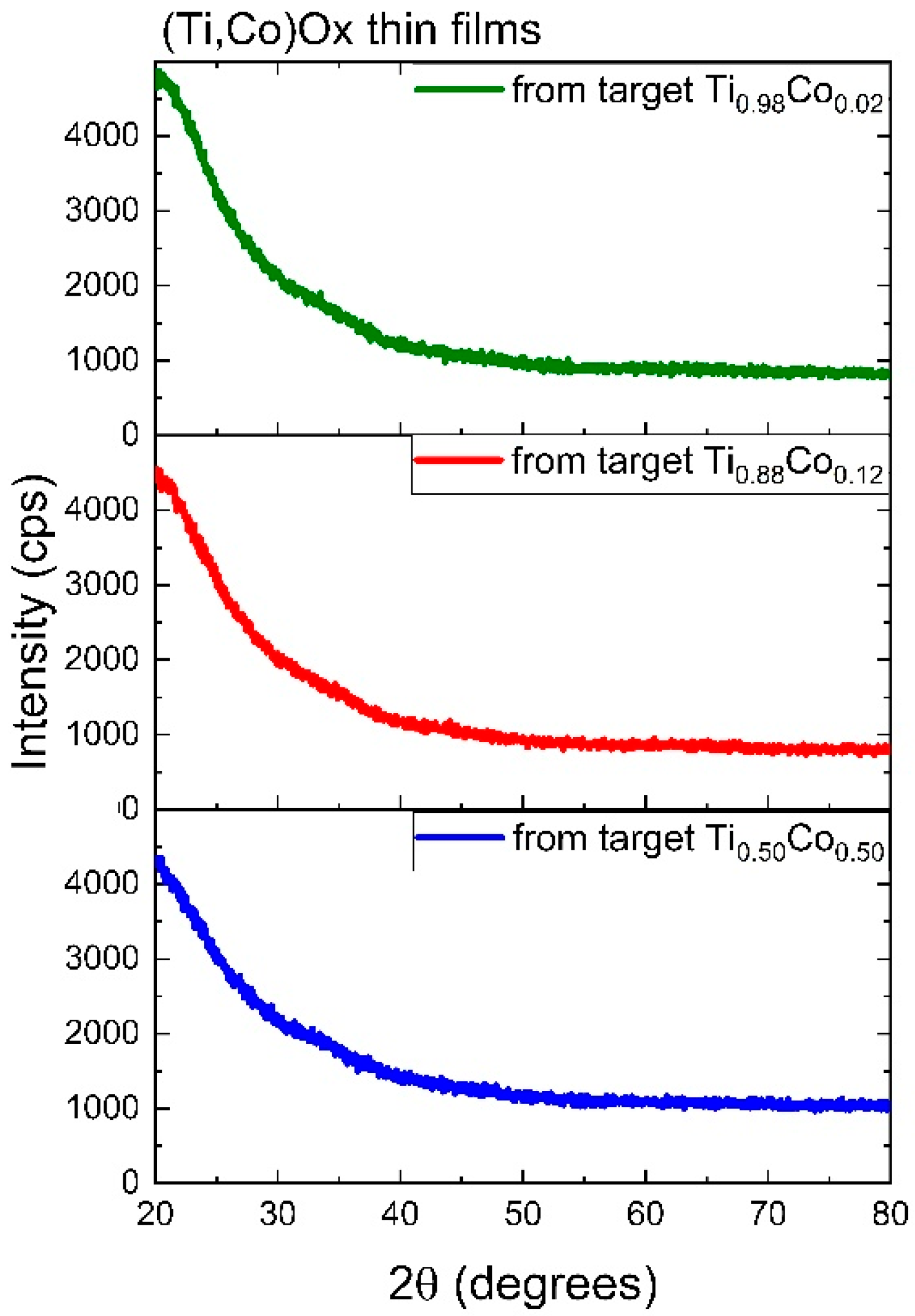
3.2.1. Structure of Oxide (Ti,Co)Ox Coatings

The influence of material composition (Co-content) on the structure of the as-deposited oxide coatings was examined by GIXRD. In Figure 7, the diffraction patterns of (Ti,Co)Ox films are shown. As it can be seen, their amorphous nature was identified. Only a background boost related to the amorphous SiO2 substrate can be observed in the 2θ range of ca. 20 ÷ 35. It should be emphasized that even for very thin coatings, their crystalline nature would be identified in grazing incidence measurements (GIXRD). In the case of pure titanium-based oxide coatings that were previously manufactured under the same conditions (described by the authors elsewhere [31,32]), a well-crystallized anatase structure (composed of crystallites with an average size less than 10 nm) was observed. This means that the addition of cobalt, both in small and large quantities, causes the amorphization of thin films and prevents crystallization. Similar results were obtained by Bohoroquez et al. [33] or Quiroz et al. [24], where Co-doped TiO2 films prepared by DC magnetron sputtering were completely amorphous. The presence of such crystalline phases as Co3O4, Ti4O7, CoTiO3 and CoTi2O5 usually requires additional annealing at high temperatures (above 450 °C). However, there are reports where the inclusion of such ions with lower valence states, as Co2+ and Co3+ increases the crystallization of TiO2 as well as the anatase to rutile transition [34]. The examined (Ti,Co)Ox thin films were sputtered in Ar:O2 (70:30) plasma. Such an atmosphere is rich in oxygen enough to obtain fully oxidized TiO2 films, while the formation of cobalt oxides (also well-crystallized) requires a higher portion of oxygen during the sputtering process [35]. Besides, low Co-content may also favor the growth of TiO2:Co, permitting the diluted formation [24,35]. In our opinion, cobalt ions block the process of crystallite nucleation and prevent further ordering that resulted in the amorphous nature of the obtained films.

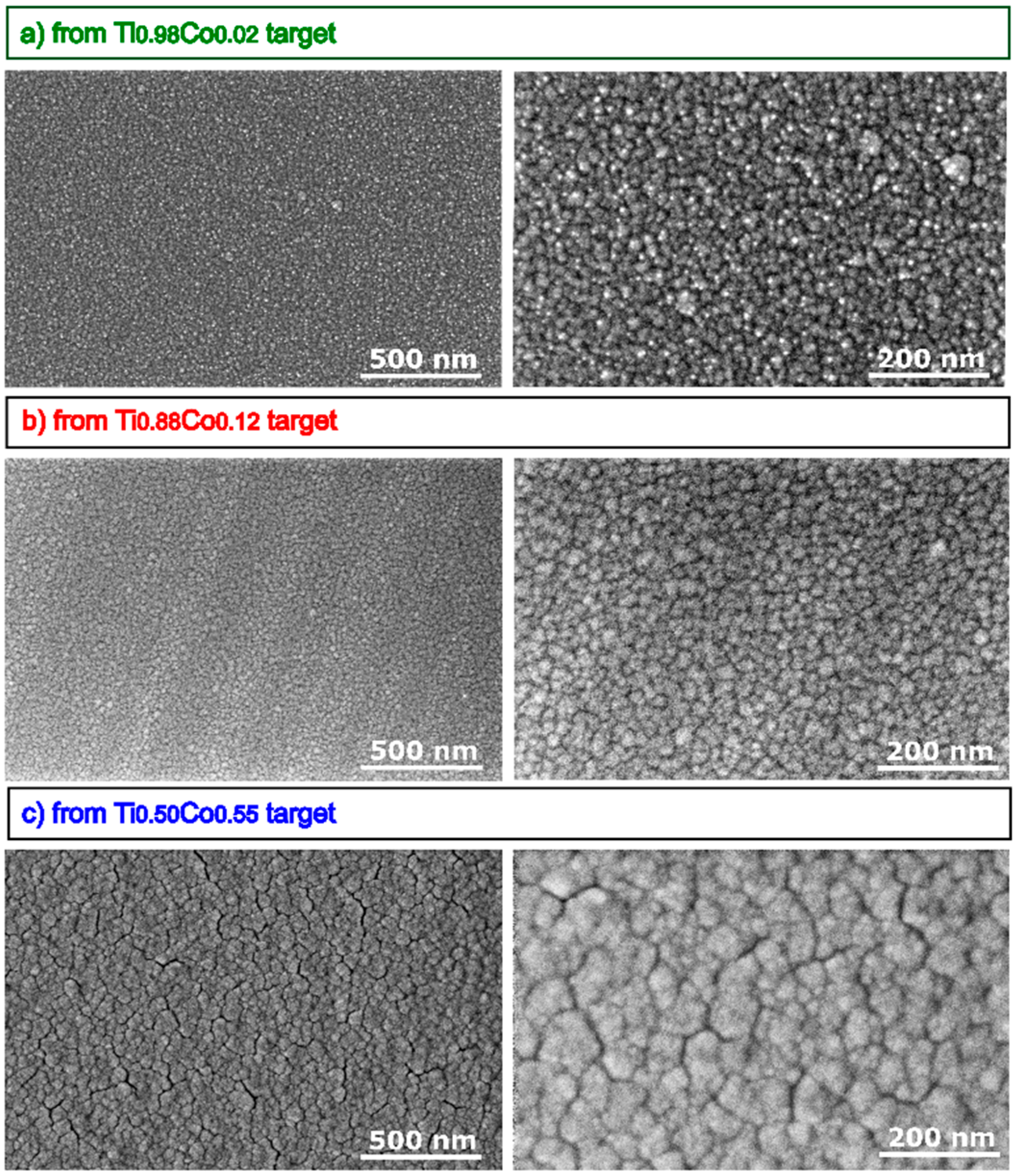
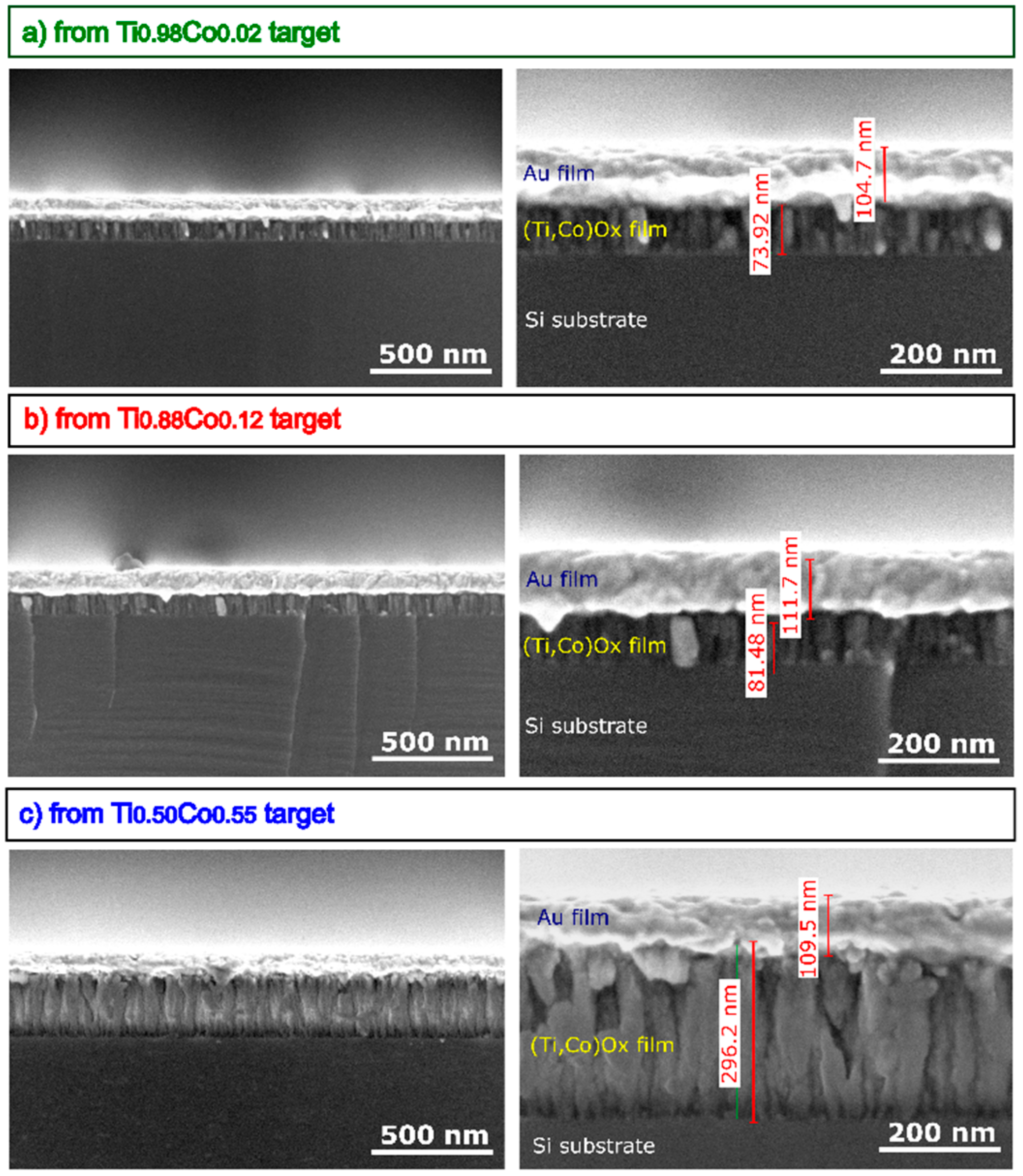
3.2.2. Microstructure and Morphology of Oxide (Ti,Co)Ox Coatings

The influence of the cobalt content on the structural properties of the oxide coatings was also investigated with the aid of SEM. For cross-section imaging, a 100 nm thick Au thin film was evaporated on the top of TiO2:Co coatings to minimize the charging effect during SEM investigation and to obtain high-resolution images. Images of the surface topography (Figure 8), as well as cross-sections (Figure 9), revealed a densely packed columnar structure of all films. In particular, as the amount of cobalt in the films increases, the width of the columns increases (on average from 20 nm to 50 nm). A similar effect can be observed on the surface, which was built from the tops of densely arranged columns. An increase in their diameter is related to the increase in Co-content. Moreover, in the case of films sputtered from targets with 2 at.% and 12 at.% of Co, their microstructure is free of cracks or voids between columns, which can be seen in the case of the film obtained from the Ti0.50Co0.50 target. Based on SEM images, the deposition in the so-called “T zone” or “transition zone” can be identified, which is characterized by the presence of very small and elongated grains due to the superficial diffusion contribution to the species mobility among grains [36]. The characters of the nucleation process, associated with the substrate temperature and deposition method, indicate the random distribution of cobalt ions in the TiO2 matrix. Such conclusions were also reached in the work of Quiroz et al. [24]. Moreover, other works in the literature on TiO2:Co also indicate the effect of fine crystallinity of the grains caused by the addition of cobalt [33,37].

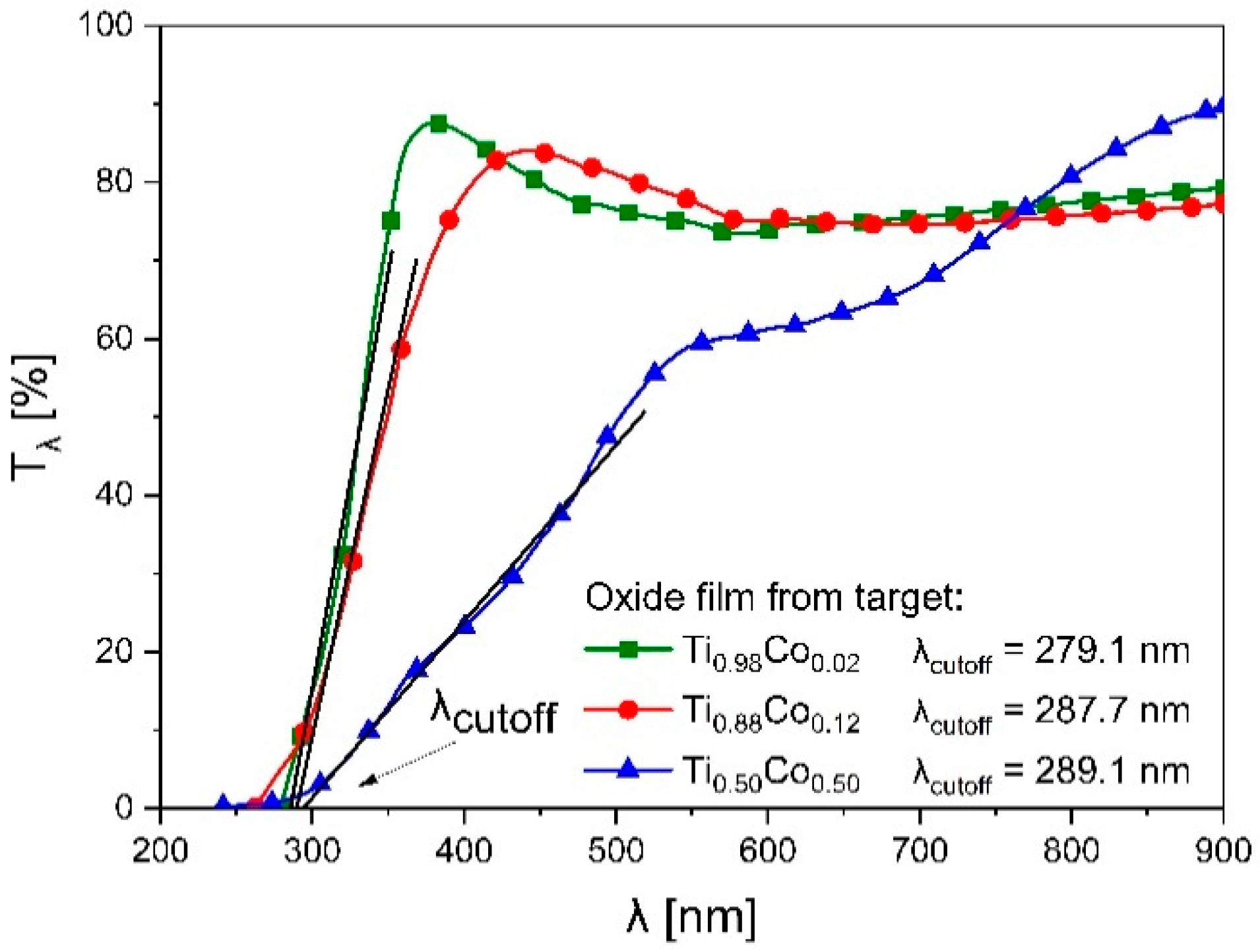
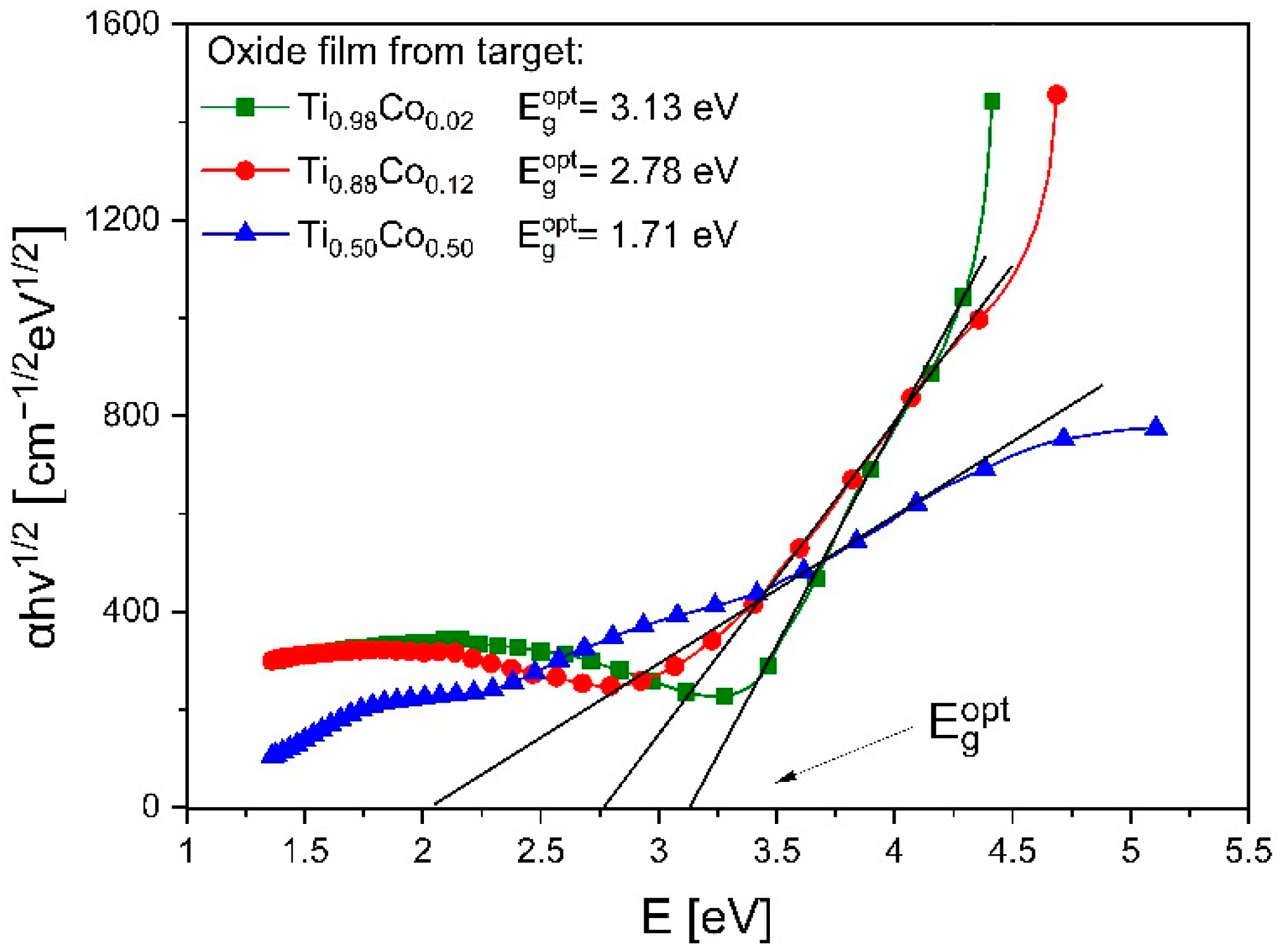
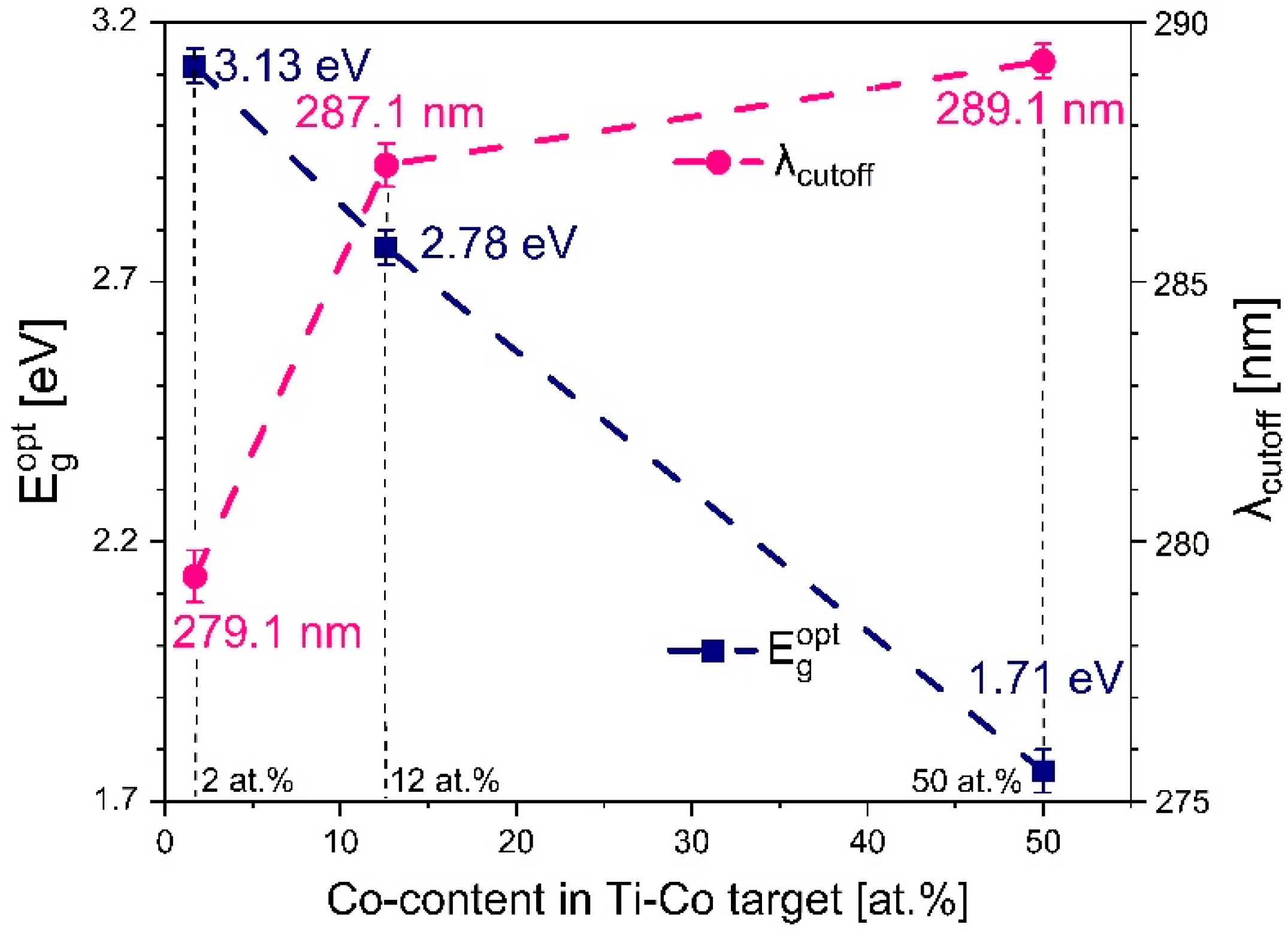
3.2.3. Optical Properties of Oxide (Ti,Co)Ox Coatings

The characterization of the optical properties of (Ti,Co)Ox coatings was performed on the basis of light transmission characteristics (Figure 10). It was found that all films exhibit high transparency. The value of Tλ=550 nm was ca. 75% for coatings deposited from Ti0.98Co0.02 and Ti0.88Co0.12 targets. However, 50 at.% of Co in the target resulted in the manufacturing of less transparent film, with transparency close to 60%. It is noteworthy that the oxide films based on titanium and cobalt are often characterized by a very low level of light transmission [33], and only their additional annealing at a temperature above 500 °C allows to obtain high transparency (usually in the range of 60% ÷ 70%).
Based on the transmission characteristics, the Tauc plots (for indirect transitions) were determined, and the optical band gap (Egopt) was estimated (Figure 11). As it can be seen, the value of Egopt was equal to 3.13 eV, 2.17 eV and 1.71 eV for the coatings as deposited from targets with 2 at.%, 12 at.% and 50 at.% of Co, respectively. This means that the greater the amount of cobalt in the (Ti,Co)Ox film, the lower the width of its optical band gap. Such effect was also noticed in other works [14,21]. In most cases, similar to the results described in this paper, an increase in the amount of cobalt causes a decrease in the Egopt value. Our results of Egopt were also presented as a function of the amount of cobalt in the target (Figure 12). They were compared with the values of the position of the optical absorption edge (λcutoff). In this case, the effect of Co-content was also observed as a so-called “red shift” (towards longer wavelengths of light). Such effect was also reported in other works. For example, Subramanian et al. [18] or Musa et al. [20] in transparent TiO2:Co films also obtained a shift of λcutoff towards longer wavelengths due to a large amount of cobalt. It should be noted that the position of the optical absorption edge is mostly determined by the manufacturing technique and the process parameters. Therefore, the “blue shift” of the λcutoff can also be found [15].

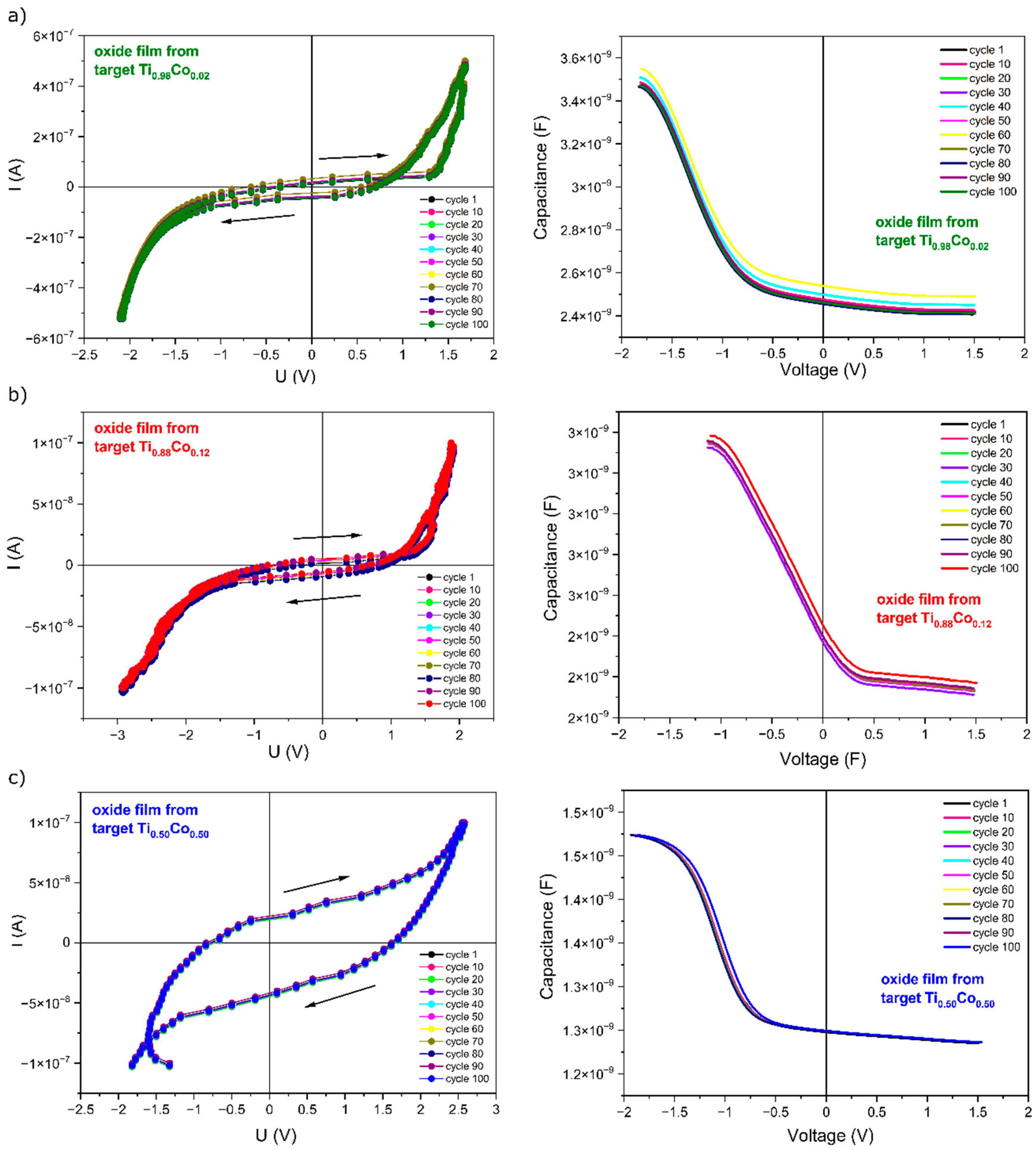
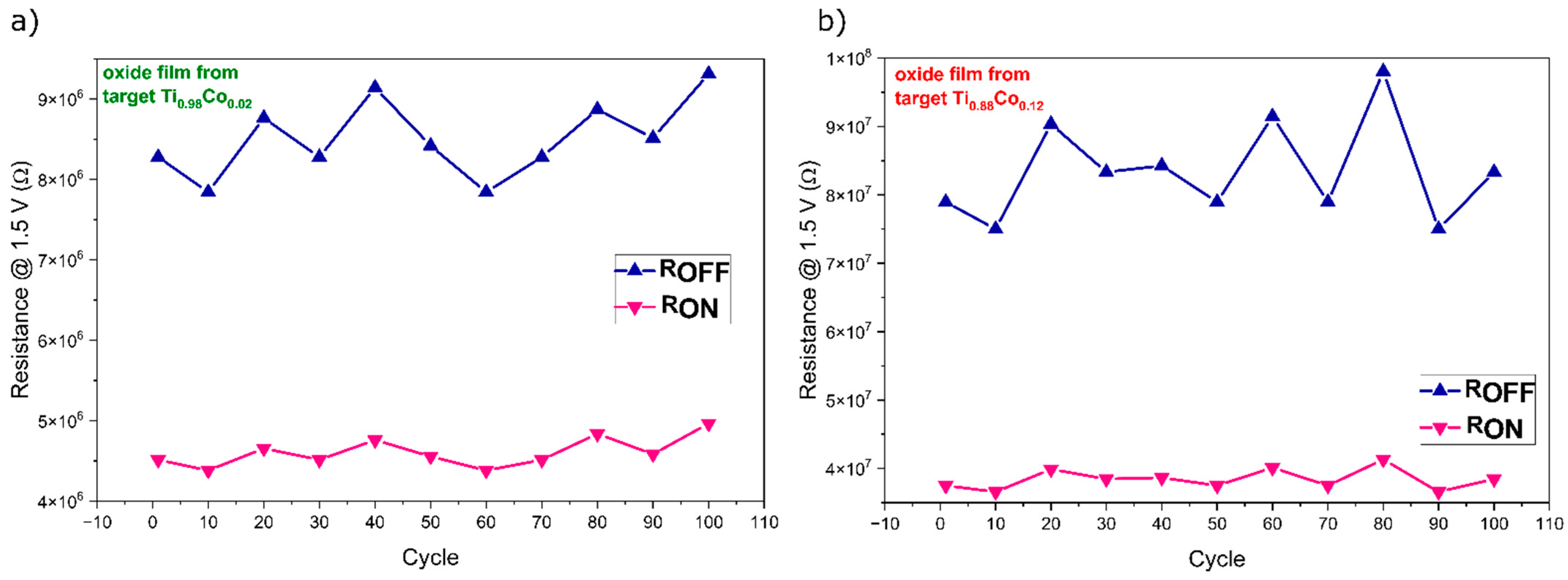
3.2.4. Electrical Properties of Oxide (Ti,Co)Ox Coatings

An investigation of electrical properties was performed for the prepared (Ti,Co)Ox thin films deposited on (p-type) silicon substrates. Additionally, a circular gold pad with 3 mm in diameter was deposited on the surface of the thin films to allow electrical measurements (Au/(TiCo)Ox/Si). That makes possible the discussion on the perspective application of prepared thin films in microelectronics. In Figure 13, the I–V characteristics measured in the transverse configuration are presented. I–V characteristics were presented in a conventional manner; the positive voltage/current values are due to the forward bias condition of the prepared structure, whereas negative values are due to the reverse bias condition.
During the measurements, the current was forced from negative to positive values and then back from the applied positive current values to the negative ones while the voltage drop was sensed using the source-measure unit (current-driven measurement). Sweeping the current allowed to observe the hysteresis loops, and as one can see in Figure 13a–c, but the shape of each of the measured curves is distinct. In the case of the structures with (Ti,Co)Ox thin films containing lower Co concentration, a unipolar memristive-like effect can be observed, which is manifested by the memory loop with forward bias polarization (Figure 13a) [38,39]. The occurrence of such effects has not been reported so far in the case of TiO2 coatings with the addition of Co. Usually, for these types of thin-film materials, a linear relationship between current and voltage is usually observed [15,20]. This means that materials based on titanium and cobalt oxides may be prospective for electronics, not only because of their spintronic application but also because of their memristive-like behavior. As it can be seen in Figure 13a, increasing the current during the measurement did not result in the change of shape of the measured characteristics until ca. 1.25 V. Above that voltage, the current suddenly increased in a relatively narrow voltage range (1.25 V ÷ 1.5 V). Changing the direction of the current flowing through the examined structure resulted in the formation of the hysteresis loop, indicating the occurrence of a memory effect. On the other hand, under the reverse bias condition, no hysteresis effect was observed, indicating the unipolar behavior of the observed phenomenon. A similar effect can be observed for the structure with (Ti,Co)Ox thin film containing about 17.6 at.% of cobalt (Figure 13b), but the memory effect, in this case, is much less pronounced (much narrower hysteresis loop). Quite unexpected results of the I–V measurement can be observed in Figure 13c. Measurements performed in similar voltage/current conditions, in this case, resulted in a visible very wide nonpinched hysteresis loop. We believe that this result was connected with a much thicker (Ti,Co)Ox thin film containing 57.2 at.% of Co, which resulted in a longer distance for electrical charge carriers that were injected from/to the metal electrode through the entire cross-section of the thin film. In this case, the observed wide hysteresis loop results rather from the polarisation and relaxation processes that occur in the thin oxide film and “charging” the structure upon switching the direction of the current flowing through it.
The capacitance-to-voltage characteristics were measured by sweeping the voltage bias from −2.0 V to 2.0 V using a 100 kHz sinusoidal measuring signal. The measurement was performed in a parallel electrical equivalent circuit. All three measured C–V curves showed a typical shape as for metal-oxide-semiconductor structures. The applied voltage sweeps the switching structure from accumulation to depletion state. Negative gate voltage at a forward bias condition causes the majority charge carriers (holes) in Si substrate to accumulate near the Si-oxide interface. Holes are injected from the Si substrate and are trapped in the oxide layer that results in a visible shift of the C–V curve toward negative voltages. For positive gate voltages, the Si-oxide interface is depleted, and in this state, the electrons from the inversion layer are injected into the oxide. Measured capacitance (c.a. 1.5 nF) in the accumulation state (oxide capacitance) was about two times lower for the structure with the highest Co-concentration (Figure 13c) than for the two remaining devices with much lower Co-concentration (c.a. 2.9 nF and 3.5 nF). This observation can be understood taking into account that the thickness of the thin film with the highest Co-concentration was more than two times higher. Measurements of current–voltage and capacitance–voltage characteristics performed for 100 equally repeated cycles testify to the high stability of the prepared thin-film structures. Additionally, retention plots for samples with switching behavior were constructed and presented in Figure 14. As one can see, in both cases, the maximum difference between RON and ROFF resistance is quite similar.

4. Conclusions

The obtained results showed that the magnetron sputtering method is successfully suitable for the repeatable manufacturing of metallic and oxide thin-film coatings based on titanium and cobalt. In the case of the above-mentioned films, the deposition processes were carried out from Ti–Co targets with 2 at.%, 12 at.% and 50 at.% of cobalt. The relation between target composition and the Co-content in the metallic and oxide films was defined. There was relatively 15–20% more cobalt in the films than in the target. The deposition rate under neutral conditions (in Ar plasma) was much higher compared to oxidizing Ar:O2 plasma. GIXRD analysis of the structural properties revealed the amorphous nature of (Ti,Co)Ox coatings, regardless of the cobalt content in the coating. The fine-grained, homogenous microstructure was identified by SEM images, where cracks and voids were identified only for films with high Co-content. Optical studies have shown that as-deposited oxide films were well transparent (60% ÷ 80%), and the Co-content had a significant impact on the transparency level decrease as well as on the “red shift” of the optical absorption edge and the decrease in Egopt (from 3.13 eV to 1.71 eV). Electrical studies revealed that in (Ti,Co)Ox thin films (with low cobalt content) deposited on Si substrate, a unipolar memristive-like effect can be observed. The occurrence of such effects has not been reported so far in the case of TiO2 coatings with the addition of Co.

Author Contributions

Conceptualization, D.W., P.P. and J.D.; methodology, D.W., M.M., J.D. and A.W.; software, D.W., M.M., K.B., T.K. and J.D.; validation, D.W., P.P. and J.D.; formal analysis, D.W., M.M., P.P. and J.D.; investigation, D.W., M.M., P.P., A.W., K.B., W.K., T.K., W.P. and J.D.; resources, D.W., J.D. and A.W.; data curation D.W., P.P. and J.D.; writing—original draft preparation, D.W., P.P. and J.D.; writing—review and editing, D.W., P.P., W.P. and J.D.; visualization, D.W., M.M., P.P. and W.K.; supervision, D.W.; project administration, J.D.; funding acquisition, J.D. All authors have read and agreed to the published version of the manuscript.

Funding

This work was co-financed from the sources given by the Polish National Science Centre (NCN) as a research project number 2018/29/B/ST8/00548.

Institutional Review Board Statement

Not applicable.

Informed Consent Statement

Not applicable.

Data Availability Statement

The data presented in this study are available in this article.

Conflicts of Interest

The authors declare no conflict of interest.

References

  1. Lin, C.-P.; Chen, H.; Nakaruk, A.; Koshy, P.; Sorrell, C.C. Effect of annealing temperature on the photocatalytic activity of TiO2 thin films. Energy Procedia 2013, 34, 627. [Google Scholar] [CrossRef] [Green Version]
  2. Mergel, D.; Buschendorf, D.; Eggert, S.; Grammes, R.; Samset, B. Density and refractive index of TiO2 films prepared by reactive evaporation. Thin Solid Film. 2000, 371, 218. [Google Scholar] [CrossRef]
  3. Kitui, M.; Mwamburi, M.M.; Gaitho, F.; Maghanga, M. Optical Properties of TiO2 based multilayer thin films: Application to optical filters. Int. J. Thin Film. Sci. Technol. 2015, 4, 17. [Google Scholar] [CrossRef]
  4. Elsaeedy, H.I.; Qasem, A.; Yakout, H.A.; Mahmoud, M. The pivotal role of TiO2 layer thickness in optimizing the performance of TiO2/P-Si solar cell. J. Alloy. Compd. 2021, 867, 159150. [Google Scholar] [CrossRef]
  5. Lyson-Sypien, B.; Radecka, M.; Rekas, M.; Swierczek, K.; Michalow-Mauke, K.; Graule, T.; Zakrzewska, K. Grain-size-dependent gas-sensing properties of TiO2 nanomaterials. Sens. Actuators B Chem. 2015, 211, 67–76. [Google Scholar] [CrossRef]
  6. Mei, J.; Liao, T.; Ayoko, G.A.; Bell, J.; Sun, Z. Cobalt oxide-based nanoarchitectures for electrochemical energy applications. Prog. Mater. Sci. 2019, 103, 596–677. [Google Scholar] [CrossRef]
  7. Verma, M.; Mitan, M.; Kim, H.; Vaya, D. Efficient photocatalytic degradation of Malachite green dye using facilely synthesized cobalt oxide nanomaterials using citric acid and oleic acid. J. Phys. Chem. Solids 2021, 155, 110125. [Google Scholar] [CrossRef]
  8. Gajbhiye, M.M.; Sharma, S.; Nigam, A.K.; Ningthoujam, R.S. Tuning of single to multi-domain behavior for monodispersed ferromagnetic cobalt nanoparticles. Chem. Phys. Lett. 2008, 466, 181–185. [Google Scholar] [CrossRef]
  9. Kaloyeros, A.E.; Pan, Y.; Goff, J.; Arkles, B. Cobalt thin films: Trends in processing technologies and emerging applications. ECS J. Solid State Sci. Technol. 2019, 8, P119. [Google Scholar] [CrossRef]
  10. Hirohata, A.; Yamada, K.; Nakatani, Y.; Prejbeanu, J.L.; Diényd, B.; Pirro, P.; Hillebrands, B. Review on spintronics: Principles and device applications. J. Magn. Magn. Mater. 2020, 509, 166711. [Google Scholar] [CrossRef]
  11. Bewan, S.; Ndolomingo, N.J.; Meijboom, R.; Bingwa, N. Cobalt oxide promoted tin oxide catalysts for highly selective glycerol acetalization reaction. Inorg. Chem. Commun. 2021, 128, 108578. [Google Scholar] [CrossRef]
  12. Švegl, F.; Orel, B.; Hutchins, M.G.; Kalcher, K. Structural and spectroelectrochemical investigations of sol-gel derived electrochromic spinel Co3O4 films. J. Electrochem. Soc. 1996, 143, 1532. [Google Scholar] [CrossRef]
  13. Bahlawane, N.; Rivera, E.F.; Kohse-Höinghaus, K.; Brechling, A.; Kleineberg, U. Characterization and tests of planar Co3O4 model catalysts prepared by chemical vapor deposition. Appl. Catal. B Environ. 2004, 53, 245. [Google Scholar] [CrossRef]
  14. Husain, S.; Alkhtaby, L.A.; Giorgetti, E.; Zoppi, A.; Maurizio Muniz, M. Influence of cobalt doping on the structural, optical and luminescence properties of sol-gel derived TiO2 nanoparticles. Philos. Mag. 2017, 97, 17. [Google Scholar] [CrossRef]
  15. Bhat, S.; Sandeep, K.M.; Kumar, P.; Dharmaprakash, S.M.; Byrappa, K. Characterization of transparent semiconducting cobalt doped titanium dioxide thin films prepared by sol–gel process. J. Mater. Sci. Mater. Electron. 2018, 29, 1098–1110. [Google Scholar] [CrossRef]
  16. Jiang, P.; Xiang, W.; Kuang, J.; Liu, W.; Cao, W. Effect of cobalt doping on the electronic, optical and photocatalytic properties of TiO2. Solid State Sci. 2015, 46, 27–32. [Google Scholar] [CrossRef]
  17. Park, Y.R.; Kim, K.J. Structural and optical properties of rutile and anatase TiO2 thin films: Effects of Co doping. Thin Solid Film. 2005, 484, 24. [Google Scholar] [CrossRef]
  18. Subramanian, M.; Vijayalakshmi, S.; Venkataraj, S.; Jayavel, R. Effect of cobalt doping on the structural and optical properties of TiO2 films prepared by sol-gel process. Thin Solid Film. 2008, 516, 3776. [Google Scholar] [CrossRef]
  19. Miao, Y.; Zhai, Z.; Jiang, L.; Shi, Y.; Yana, Y.; Duan, D.; Zhen, K.; Wang, J. Facile and new synthesis of cobalt doped mesoporous TiO2 with high visible-light performance. Powder Technol. 2014, 266, 365–371. [Google Scholar] [CrossRef]
  20. Musa, M.Z.; Ameran, Z.F.; Mamat, M.H.; Malek, M.F.; Rasheid, N.A.; Noor, U.M.; Rusop, M. Effects of cobalt doping concentration on the structural, electrical, and optical properties of titanium dioxide thin films. In Proceedings of the Institute of Electronics Engineers, 2011 International Conference on Electronic Devices, Systems and Applications (ICEDSA), Mid Valley City, Malaysia, 25–27 April 2011. [Google Scholar] [CrossRef]
  21. Islam, N.M.; Podder, J. The role of Al and Co co-doping on the band gap tuning of TiO2 thin films for applications in photovoltaic and optoelectronic devices. Mater. Sci. Semicond. Process. 2021, 121, 105419. [Google Scholar] [CrossRef]
  22. Huo-ping, Z.; Nan-nan, X.; Gong-ping, L.; Tian-jing, L.; Xing-xin, G.; Jing-sheng, C. The magnetic properties and microscopic structural of a ferromagnetic semiconductor: Rutile TIO2 single crystals implanted with cobalt ions. Surf. Coat. Technol. 2013, 229, 109–111. [Google Scholar] [CrossRef]
  23. Ganshina, E.A.; Granovsky, A.B.; Orlov, A.F.; Perov, N.S.; Vashuk, M.V. Magneto-optical spectroscopy of diluted magnetic oxides TiO2−δ: Co. J. Magn. Magn. Mater. 2009, 321, 723–725. [Google Scholar] [CrossRef]
  24. Quiroz, H.P.; Galíndez, E.F.; Dussan, A. Ferromagnetic-like behavior of Co doped TiO2 flexible thin films fabricated via co-sputtering for spintronic applications. Heliyon 2020, 6, e03338. [Google Scholar] [CrossRef] [PubMed] [Green Version]
  25. Yu, H.; Ni, L.; Wang, Y. Non-Volatile In-Memory Computing by Spintronics; Morgan & Claypool Publishers: Williston, VT, USA, 2017; pp. 13–14. [Google Scholar]
  26. Lei, C.; Du, Y.; Zhu, M.; Huo, W.; Wu, H.; Zhang, Y. Microstructure and mechanical properties of in situ TiC/Ti composites with a laminated structure synthesized by spark plasma sintering. Mater. Sci. Eng. A 2021, 812, 141136. [Google Scholar] [CrossRef]
  27. Wimler, D.; Lindemann, J.; Gammer, C.; Spoerk-Erdely, P.; Stark, A.; Clemens, H.; Mayer, S. Novel intermetallic-reinforced near-α Ti alloys manufactured by spark plasma sintering. Mater. Sci. Eng. A 2020, 792, 139798. [Google Scholar] [CrossRef]
  28. Depla, D.; De Gryse, R. Target poisoning during reactive magnetron sputtering: Part I: The influence of ion implantation. Surf. Coat. Technol. 2004, 183, 184–189. [Google Scholar] [CrossRef]
  29. Waite, M.M.; Ismat Shah, S.I. Target poisoning during reactive sputtering of silicon with oxygen and nitrogen. Mater. Sci. Eng. B 2007, 140, 64–68. [Google Scholar] [CrossRef]
  30. Arif, M.; Eisenmenger-Sittner, C. In situ assessment of target poisoning evolution in magnetron sputtering. Surf. Coat. Technol. 2017, 324, 345–352. [Google Scholar] [CrossRef]
  31. Wiatrowski, A.; Mazur, M.; Obstarczyk, A.; Kaczmarek, D.; Pastuszek, R.; Wojcieszak, D.; Grobelny, M.; Kalisz, M. Influence of magnetron powering mode on various properties of TiO2 thin films. Mater. Sci. Pol. 2018, 36, 748–760. [Google Scholar] [CrossRef] [Green Version]
  32. Wiatrowski, A.; Mazur, M.; Obstarczyk, A.; Wojcieszak, D.; Kaczmarek, D.; Morgiel, J.; Gibson, D. Comparison of the physicochemical properties of TiO2 thin films obtained by magnetron sputtering with continuous and pulsed gas flow. Coatings 2018, 8, 412. [Google Scholar] [CrossRef] [Green Version]
  33. Bohórquez, A.J.; Quiroz, H.P.; Dussan, A. Growth and crystallization of Cobalt-doped TiO2 alloys: Effect of substrate and annealing temperature. Appl. Surf. Sci. 2019, 474, 97. [Google Scholar] [CrossRef]
  34. Rao, C.N.R.; Subba Rao, G.V. Transition Metal Oxides—Crystal Chemistry, Phase Transition and Related Aspects; 1974 U.S. Department of Commerce, Michigan, National Bureau of Standards. Available online: http://refhub.elsevier.com/S2405-8440(20)30183-3/sref26 (accessed on 1 March 2021).
  35. NIST Laboratory. Co Oxides Structure; 2019. Available online: https://srdata.nist.gov/xps/main_search_menu.aspx (accessed on 15 February 2021).
  36. Thornton, J.A. Structure-zone models of thin films. Model. Opt. Thin Film. 1988, 0821. [Google Scholar] [CrossRef]
  37. Quiroz, H.P.; Dussan, A. Synthesis temperature dependence on magnetic properties of cobalt doped TiO2 thin films for spintronic applications. Appl. Surf. Sci. 2019, 484, 688–691. [Google Scholar] [CrossRef]
  38. Domaradzki, J.; Wojcieszak, D.; Kotwica, T.; Mańkowska, E. Memristors: A short review on fundamentals, structures, materials and applications. Int. J. Electron. Telecommun. 2020, 66, 373–381. [Google Scholar] [CrossRef]
  39. Domaradzki, J.; Kotwica, T.; Mazur, M.; Kaczmarek, D.; Wojcieszak, D. Memristive properties of transparent oxide semiconducting (Ti,Cu)Ox-gradient thin film. Semicond. Sci. Technol. 2018, 33, 015002. [Google Scholar] [CrossRef]
Figure 1. Microstructure with WDS maps of elemental distribution of Ti and Co in sintered targets: (a) Ti0.98Co0.02, (b) Ti0.88Co0.12, (c) Ti0.50Co0.50.
Materials 14 03797 g001
Figure 2. Images of surface topography with marked areas of EDS analysis for metallic Ti–Co thin films as deposited from: (a) Ti0.98Co0.02, (b) Ti0.88Co0.12, (c) Ti0.50Co0.50 targets; with (d) a diagram of the dependence between Co-content in the target and in the metallic film.
Materials 14 03797 g002
Figure 3. SEM images of surface topography with EDS maps of elemental distribution for oxide (Ti,Co)Ox thin films as deposited from: (a) Ti0.98Co0.02, (b) Ti0.88Co0.12, (c) Ti0.50Co0.50 targets; with (d) a diagram of the dependence between Co-content in the target and in the oxide film.
Materials 14 03797 g003
Figure 4. Three-dimensional profiles of metallic Ti–Co and oxide (Ti,Co)Ox thin films prepared by magnetron sputtering from different targets.
Materials 14 03797 g004
Figure 5. The influence of the Co-content in the Ti–Co target on the roughness of metallic and oxide thin films. Designation: Sq—root mean square roughness.
Materials 14 03797 g005
Figure 6. The influence of the Co-content in the Ti–Co target on the sputtering rate (SR) for metallic and oxide thin films.
Materials 14 03797 g006
Figure 7. GIXRD patterns of oxide (Ti,Co)Ox thin films as deposited from different targets.
Materials 14 03797 g007
Figure 8. SEM images of surface of (Ti,Co)Ox thin films prepared from: (a) Ti0.98Co0.02, (b) Ti0.88Co0.12, (c) Ti0.50Co0.50 targets.
Materials 14 03797 g008
Figure 9. SEM images of cross-section of (Ti,Co)Ox thin films prepared from: (a) Ti0.98Co0.02, (b) Ti0.88Co0.12, (c) Ti0.50Co0.50 targets (with Au layer on top).
Materials 14 03797 g009
Figure 10. Transmission characteristics of (Ti,Co)Ox thin films prepared from different targets. Designations: Tλ—light transmission coefficient, λcutoff—position of the optical absorption edge.
Materials 14 03797 g010
Figure 11. Tauc plots for (Ti,Co)Ox thin films prepared from different targets. Designations: Egopt—optical band gap.
Materials 14 03797 g011
Figure 12. Influence of Co-content in the Ti–Co target on the optical band gap (Egopt) and position of the optical absorption edge (λcutoff) of (Ti,Co)Ox thin films.
Materials 14 03797 g012
Figure 13. Current to voltage (I–V) and capacitance to voltage (C–V) characteristics of prepared Au/(Ti,Co)Ox/Si structures with different cobalt concentration—prepared from: (a) Ti0.98Co0.02, (b) Ti0.88Co0.12, (c) Ti0.50Co0.50 targets.
Materials 14 03797 g013
Figure 14. Retention plots of prepared Au/(Ti,Co)Ox/Si structures with different cobalt concentration—prepared from: (a) Ti0.98Co0.02 and (b) Ti0.88Co0.12 targets.
Materials 14 03797 g014
Table 1. Material composition of thin-film coatings (metallic and oxide) based on Ti and Co and targets used for their deposition by magnetron sputtering.
TargetCo-Content [at.%]
In the TargetIn the Film
Metallic (Ti–Co)Oxide (Ti,Co)Ox
Ti0.98Co0.021.73.51.8
Ti0.88Co0.1212.619.417.6
Ti0.50Co0.5050.260.757.2
Publisher’s Note: MDPI stays neutral with regard to jurisdictional claims in published maps and institutional affiliations.

