1. Introduction
Since the 1980s, the use of NF
3 plasmas in semiconductor, display, and solar cell processing applications has been investigated [
1]. NF
3 plasma is used to etch various thin films under reactive ion etching (RIE) conditions [
2,
3] or to clean a plasma-enhanced chemical vapor deposition (PECVD) chamber [
4,
5]. Cleaning the PECVD chamber is performed by supplying ions and radicals for cleaning through a remote plasma source (RPS) [
6] or by directly supplying ions and radicals through an in situ plasma discharge [
7]. In addition, NF
3 is attracting attention as a new etching technology, such as cryogenic electron beam induced etching (EBIE) [
8,
9] and highly selective etching [
10]. NF
3 has a high etch rate, etching efficiency, and a relatively high chemical stability [
2,
11]. Accordingly, the use of NF
3 is significantly increasing every year. However, NF
3 is a greenhouse gas with a very high global warming potential of 16,100 and a lifespan of 500 years [
12]. The contribution of NF
3 to the radiative forcing in the Earth’s atmosphere is very small, ~0.01%, in 2011, but the use of NF
3 is increasing every day; therefore, this number continues to increase [
13]. The share of NF
3 in fluorinated gases increased from 13–28% in 2005 to 17–36% in 2010, and NF
3 is currently the most widely used and released fluorinated gas [
1,
14]. Thus, it was included in the second commitment period of the Kyoto Protocol as the seventh greenhouse gas whose emissions are to be regulated [
15].
Studies have been conducted to replace NF
3 [
16,
17]. Among them, F
3NO was considered a candidate gas to replace NF
3 [
18]. Similar to NF
3, F
3NO does not contain perfluorocarbons. In addition, because its molecule has an N=O bond, its atmospheric life is relatively short, and thus, its contribution to global warming is expected to be less than that of NF
3. The etch rate of F
3NO is almost the same as that of NF
3. However, further studies on F
3NO have not been conducted, and information on the mechanism occurring in the F
3NO plasma during the cleaning process is insufficient. Therefore, research on the F
3NO plasma to replace NF
3 is urgently needed.
The present study focused on evaluating and analyzing the properties of F3NO plasma. Accordingly, the cleaning abilities of NF3 and F3NO were compared, and the characteristics of the F3NO plasma were analyzed. The cleaning ability of the F3NO plasma was evaluated by etching a SiO2 film previously deposited on a Si wafer sample. Although the etching time of the small sample and the cleaning time of the PECVD chamber may not coincide, it was considered suitable for the evaluation of the cleaning ability of the gas. To analyze the etch mechanism, the etching plasma was diagnosed using a residual gas analyzer (RGA) and a high-voltage probe. The reactions in the F3NO plasma were predicted by comparing the types and intensity of ions generated in the NF3 and F3NO plasmas. In addition, the etch rates of the SiO2 thin film using the NF3 and F3NO plasmas were compared to confirm whether the F3NO plasma can replace NF3.
3. Results and Discussion
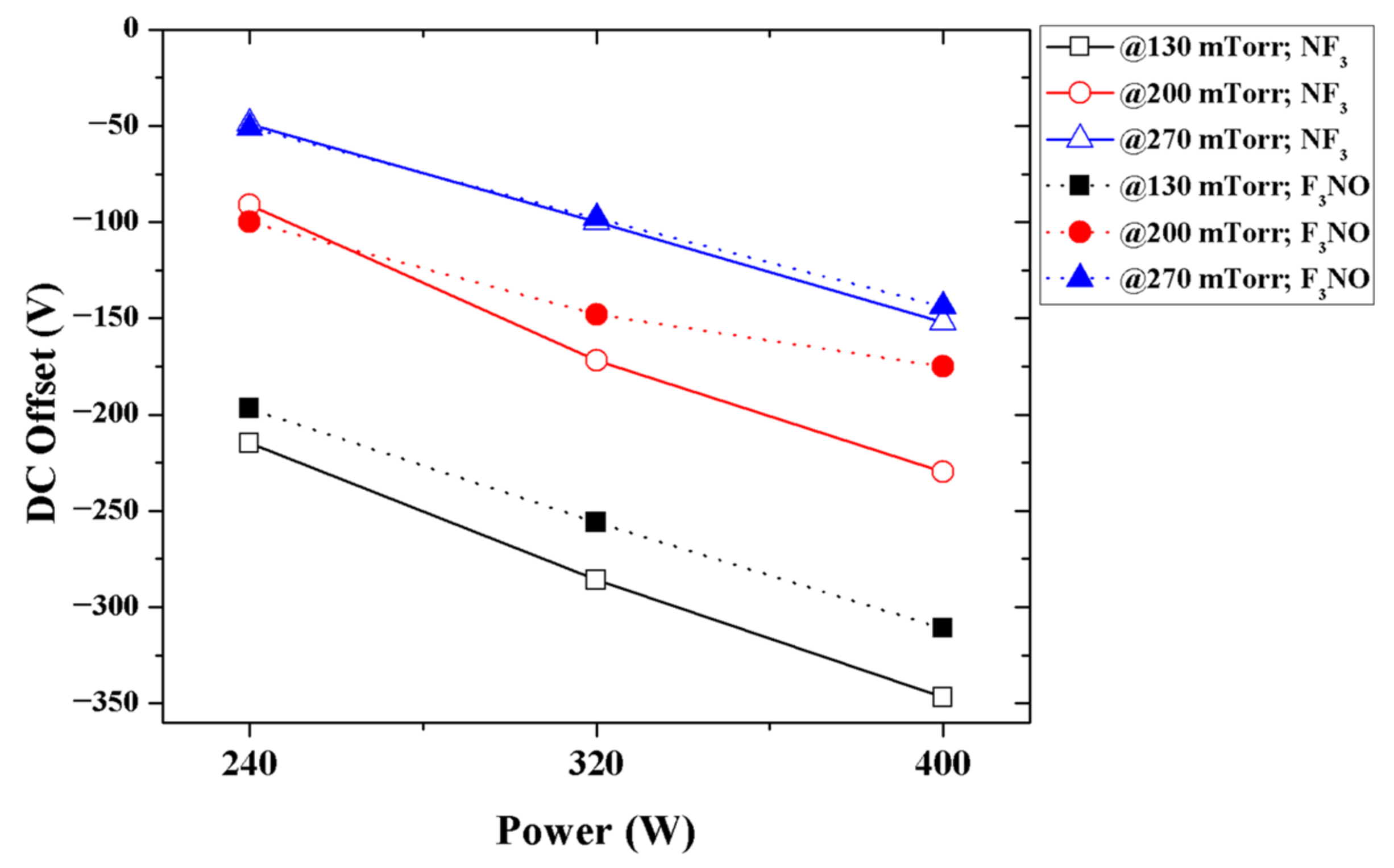
To compare the characteristics of the NF
3 and F
3NO plasmas and to understand the characteristics of the latter, a DC offset measurement during the RIE plasma discharge was performed (
Figure 2). The F
3NO plasma showed a similar DC offset value very close to that of the NF
3 plasma.
The NF
3 plasma has a very high electronegativity [
21,
22]. Therefore, when compared with fluorocarbon plasmas, the NF
3 plasma shows a relatively low DC offset value. Plasma with a high electronegativity tends to be unstable and easily collapses. In this case, the NF
3 plasma is discharged only in a part of the chamber, and the plasma collapses in other parts; therefore, these parts may not be exposed to the plasma. Alternatively, a constant discharge may not occur but may flicker and cause discharge.
The comparison results of the DC offset of the NF
3 and F
3NO plasmas show that the electronegativity of the F
3NO plasma can also be quite considerable. In the case of the NF
3 plasma, an inert gas (e.g., He, Ar) was diluted and discharged to increase the stability and uniformity of the plasma and enhance etch rates [
23,
24,
25,
26]. Inert gases rarely participate in chemical reactions in the plasma but can have a great influence on the discharge process. The DC offset result indicates that the characteristics of the F
3NO plasma can also be comparable to those of the NF
3 plasma. Thus, in future studies, dilution with an inert gas, such as Ar, is recommended.
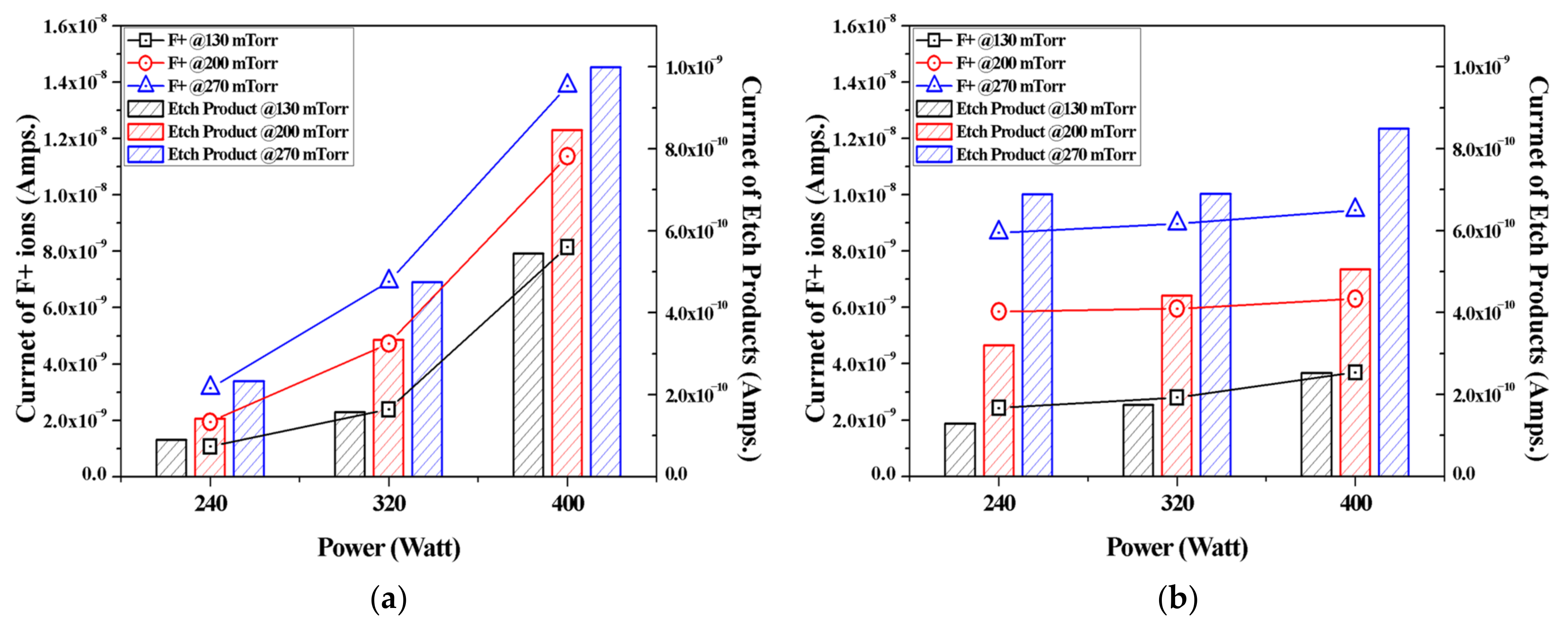
Figure 3 shows the current of F+ ions and etch products (SiF, SiF
2, and SiF
3) generated from the NF
3 and F
3NO plasmas when etching SiO
2 thin films. As the pressure and power increased, the intensity of the peak of F ions and the etch product also increased. At this time, when the pressure or discharge power was low, more F ions were generated in the F
3NO plasma than in the NF
3 plasma. In addition, the lower the discharge power, the higher the generation of etch products in F
3NO than in NF
3. These findings confirmed that the etching of F
3NO occurs more actively at low power and pressure. In addition, as the power increases, the intensity of F ions in NF
3 rapidly increases, whereas in the F
3NO plasma, the F ions gradually increase even if the discharge power of F increases. As will be shown further, this trend is similar for other ions as well. Consequently, the plasma density of F
3NO reacts more slowly to the change of the discharge power compared to NF
3.
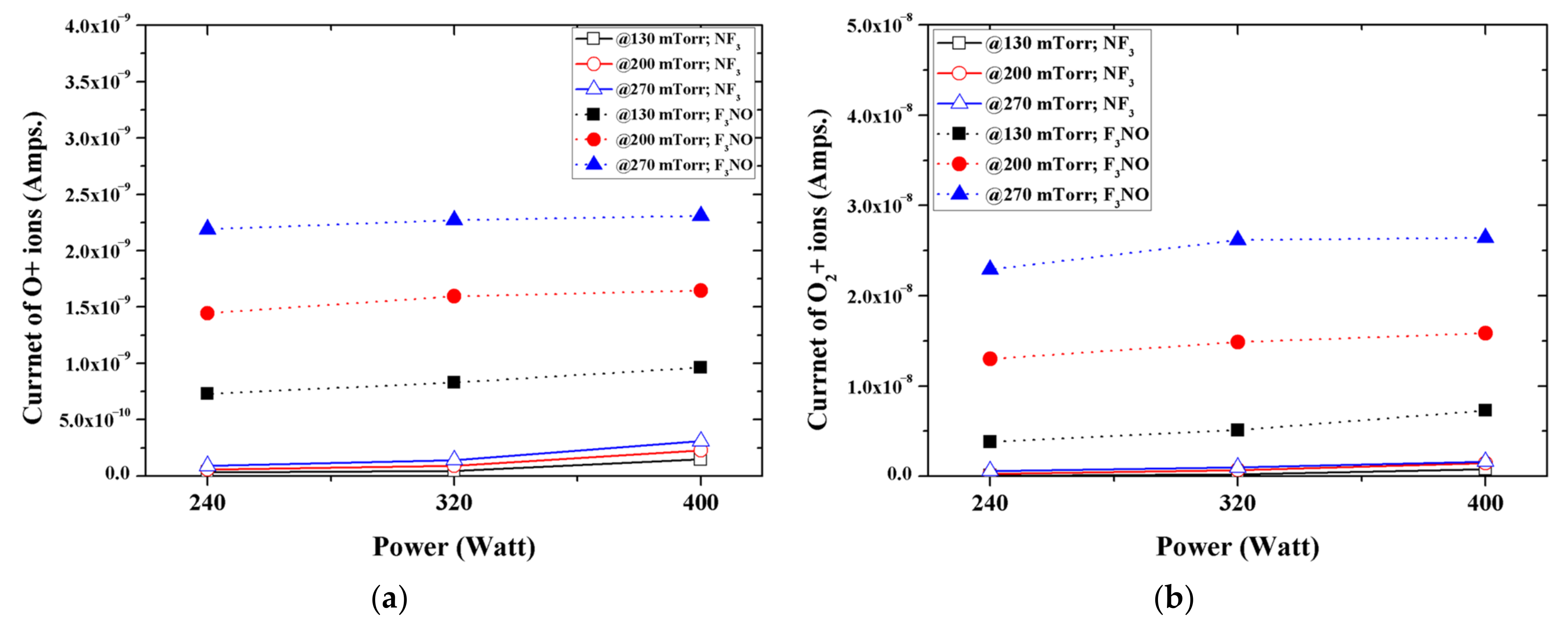
Among the ions generated in the NF
3 and F
3NO plasmas during the silicon oxide thin film etching, O and O
2 were more common in the F
3NO plasma under all conditions (
Figure 4). Compared with the F
3NO plasma, O and O
2 ions hardly occurred in the NF
3 plasma. In the case of the F
3NO plasma, O and O
2 ions were simultaneously generated by O contained in F
3NO and O
2 gas already present in the chamber, whereas the NF
3 plasma generated O and O
2 ions only from O
2 gas existing in the base. Therefore, when the pressure increased, the intensity of O and O
2 ions generated in the NF
3 plasma was almost unchanged, whereas in the F
3NO plasma, when the pressure increased, O and O
2 ions appeared to rapidly increase compared to the NF
3 plasma.
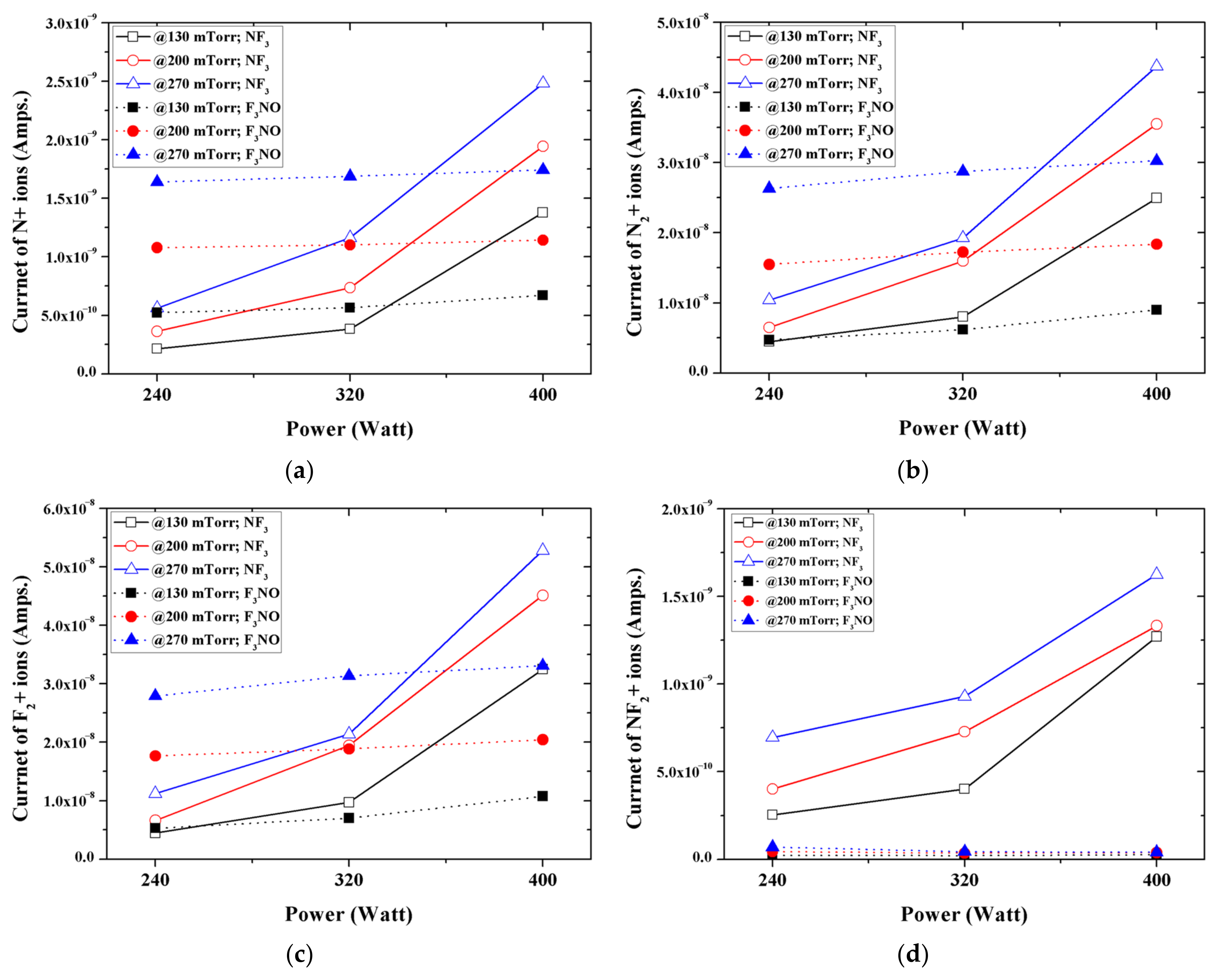
Figure 5 shows the peak intensities of the major ions generated in the NF
3 and F
3NO plasmas during the etching of a silicon oxide thin film. N, N
2, and F
2 ions occurred more in F
3NO at low discharging powers and more in NF
3 at higher discharging powers. Conversely, NF
2 ions occurred more in the NF
3 plasma under all conditions.
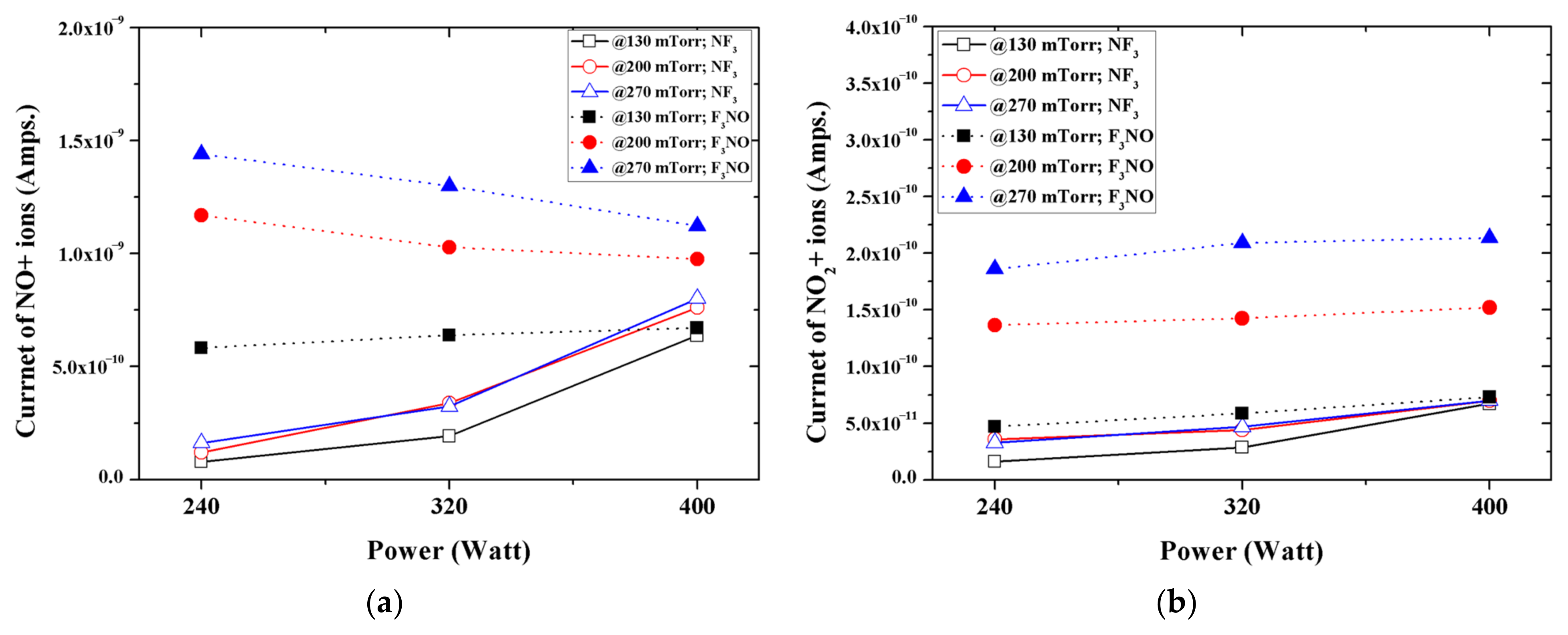
Figure 6 shows the intensity of NO and NO
2 ions generated in the NF
3 and F
3NO plasmas during the etching of silicon oxide thin films. When the discharge power was low, the NO ions generated in the F
3NO plasma were more than those of the NF
3 plasma (numerical value). However, as the discharge power increased, the number of NO ions in the F
3NO plasma gradually decreased, whereas those in the NF
3 plasma rapidly increased and became almost the same as the peak intensity of NO ions generated in the F
3NO plasma. Conversely, many more NO
2 ions occurred in the F
3NO plasma under all conditions.
Metastable N
2 is produced mostly by collisions with a high-energy electron, making the mechanism more significant in an electronegative gas discharge, such as NF
3 and F
3NO. At a higher discharge power, higher energy electrons are supplied, thus increasing the density of NO ions [
27]:
A reaction involving atomic nitrogen that resulted in a different density of NO ions in the F
3NO plasma and the NF
3 plasma was more important in an oxygen-rich plasma [
28,
29]. As shown in
Figure 4a, because F
3NO is an oxygen-rich plasma, reaction (2) became significant, and a large amount of NO ions were produced.
In the F
3NO plasma, NF is decomposed through the following reaction.
The species produced in the primary reactions led to secondary reactions which formed NO
2 ions through the following exothermic reactions:
In the case of the NF3 plasma, the above reaction is not significant because the number of O ions is remarkably small, but F3NO causes a more significant reaction. Therefore, the number of NF2 and NF ions are fewer in the F3NO plasma than in the NF3 plasma, whereas ions such as N, N2, and F are present in similar amounts in the F3NO plasma and the NF3 plasma.
In the NF
3 plasma, NO ions may be generated through the bonding of O and N ions, which are etching by-products, or through a process in which N ions form Si–O–N bonding on the surface of the silicon oxide thin film [
30]. In the F
3NO plasma, NO is formed by the N and O ions contained in F
3NO. In the case of F
3NO, this condition becomes the main mechanism. NO formed in this way forms NO
2 through the following reaction:
In the NF3 plasma, because the number of O ions was remarkably small, this oxidation reaction occurred only to a small extent. Conversely, in the F3NO plasma, as the number of O ions was much larger, the extent of the oxidation reaction was more significant. When the discharge power was increased, the number of NO formed was almost unchanged, but the peak of NO ions decreased due to the considerable oxidation of NO.
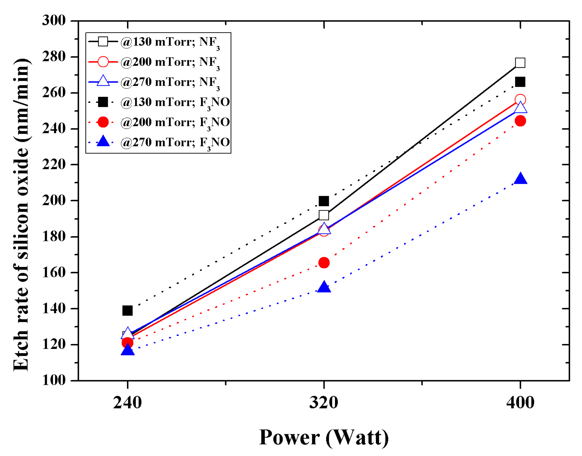
Figure 7 shows the SiO
2 etch rate according to the discharge power and process pressure. The results imply that the lower the pressure and discharge power, the higher the etch rate of F
3NO. This is because when the pressure and discharge power is low, chemical etching occurs more easily because the number of F ions generated is greater in F
3NO. Conversely, the DC offset at a low power has a small absolute value for the NF
3 and F
3NO plasmas; therefore, the ion bombardment energy does not have a significant effect on etching. When the discharge power was increased, the DC offset value of the NF
3 plasma became larger than that of the F
3NO plasma, so the etch rate of NF
3 also became higher. When the discharge pressure and discharge power increased, the intensity of F ions also increased as NF
3 increased, so the etch rate decreased in F
3NO. Furthermore, the etch rate of silicon oxide during F
3NO plasma etching was approximately 95.0% of the rate during NF
3 plasma etching.
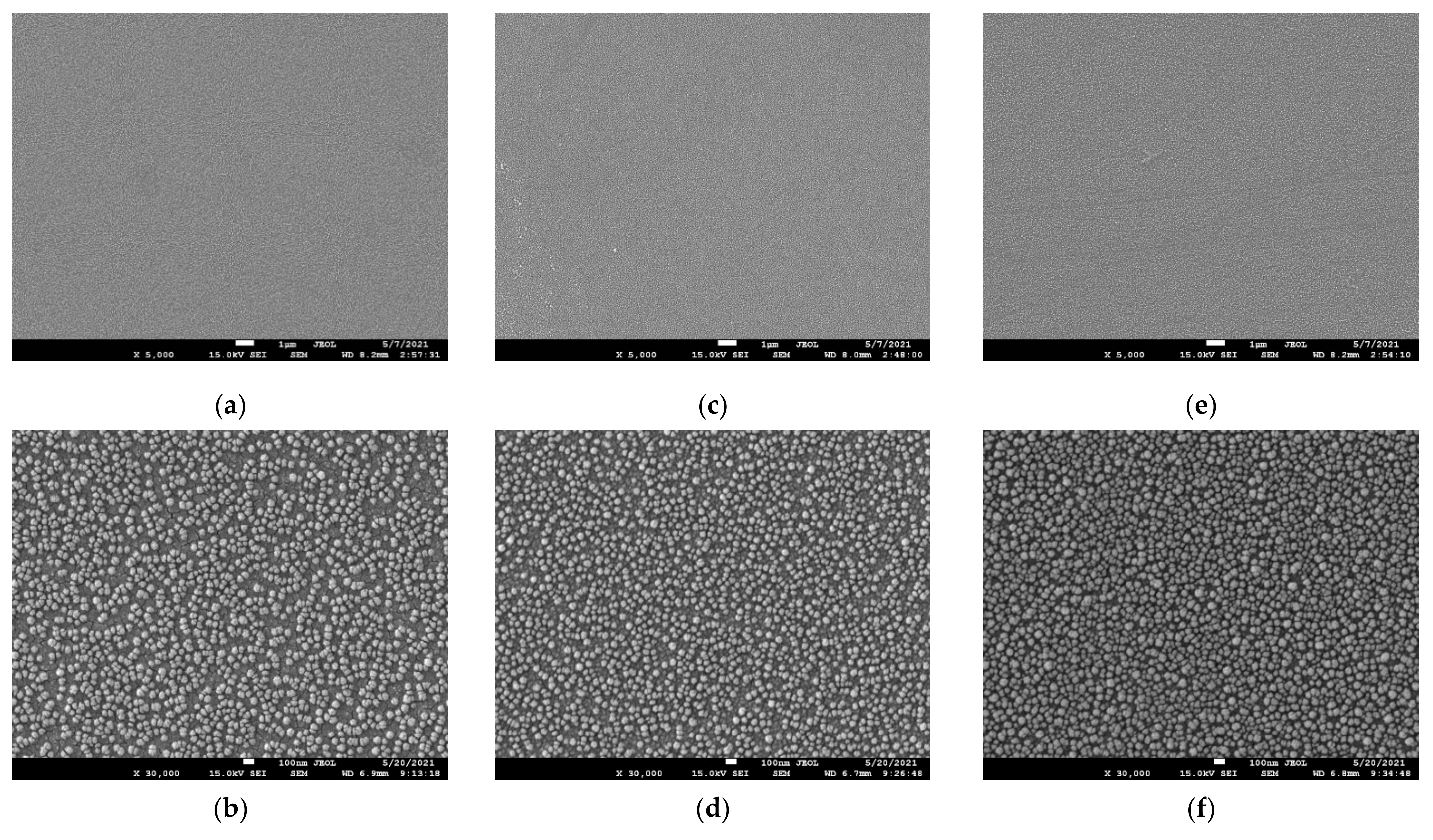
We performed SEM measurements to determine whether O or N ions present in the plasma had a negative effect on the etching quality.
Figure 8 shows a SiO
2 surface of SEM images after the etching process at 400 W discharge power and 270 mTorr pressure. For accurate SEM measurements, a platinum coating was applied on the surface by sputtering. The round shape particles in the figures are platinum nanoparticles from the platinum coating. The size of these nanoparticles is in order of several nanometers. Besides platinum nanoparticles, no other structures such as cracks or holes were found on the surface. No significant difference was observed between the SEM images of the unprocessed and processed surface of SiO
2. Therefore, it was confirmed that O or N ions in F
3NO did not have a negative effect on the etching quality.
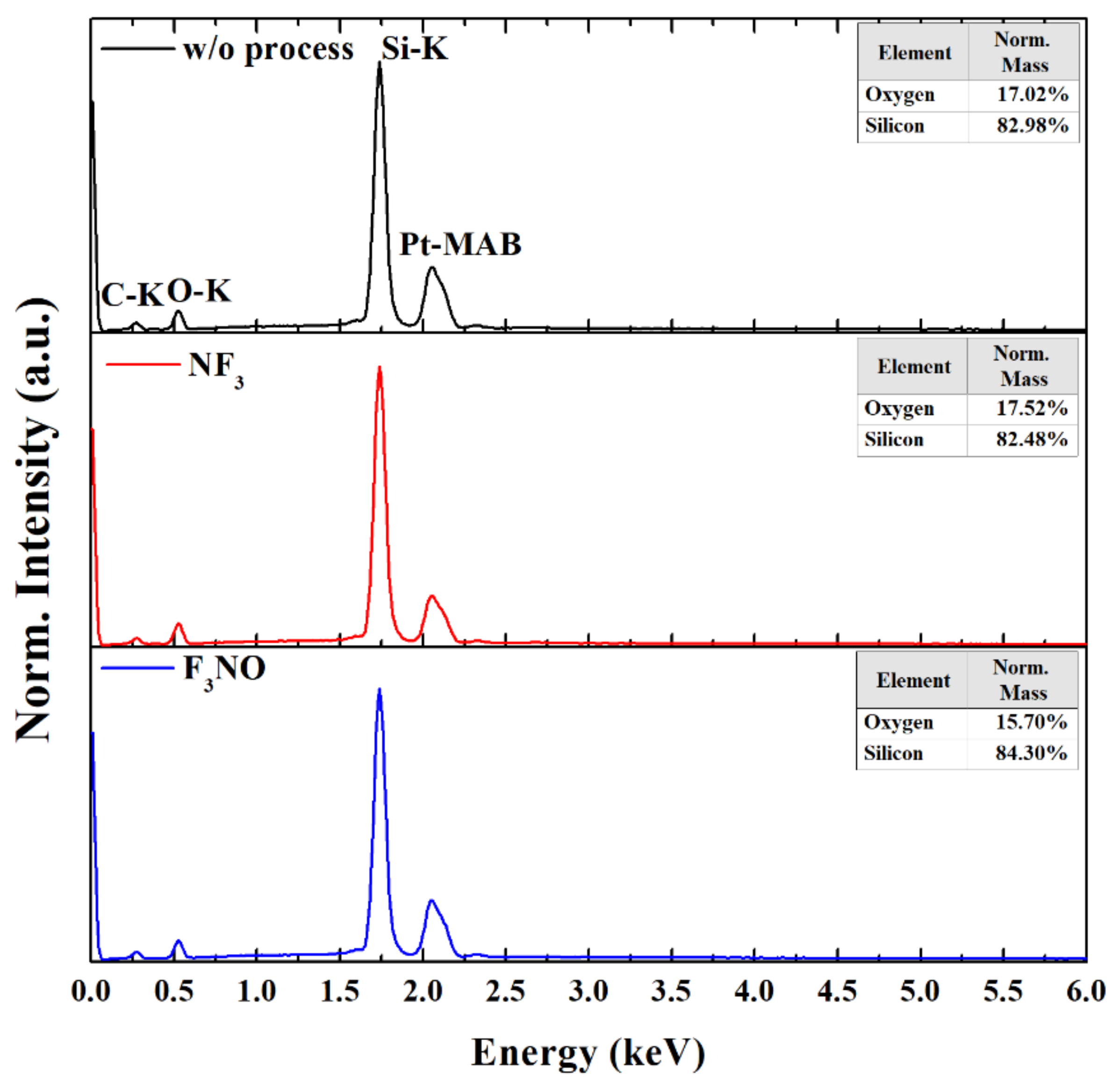
Figure 9 shows EDS spectra of the SiO
2 surface without process and after etching at a 400 W discharge power and 270 mTorr pressure with the NF
3 and F
3NO plasmas. The C peak in the EDS spectra was caused either by carbon contamination or by the window in the detector. Except for carbon and platinum (from the platinum coating), no peaks other than O and Si were found in the EDS spectra. This indicates that nitrogen, oxygen, or NO did not chemically contaminate the SiO
2 surface during the etching process.
The mass ratio of silicon and oxygen is noticeable in the EDS spectra. The mass ratio of silicon and oxygen on the SiO
2 surface is almost the same when the process is not performed and when the NF
3 etching process is performed. However, the mass ratio of O appears less on the SiO
2 surface after F
3NO etching. This may be caused by the following reaction on the SiO
2 surface during F
3NO etching.
As above, NO ions absorb O in the SiO
2 surface to decrease surface oxidation [
31]. Therefore, the F
3NO etched SiO
2 surface has a smaller oxygen mass ratio than the NF
3 etched SiO
2 surface. Moreover, this de-oxidation process increases the Si etching rate, especially during etching with F
3NO at low pressure and low power with a significant quantity of NO ions.
4. Conclusions
The DC offset was measured during NF3 and F3NO plasma discharges. Compared with the DC offset of the NF3 plasma, the F3NO plasma showed an almost similar DC offset value. This finding confirms that the F3NO plasma, similar to the NF3 plasma, can have a very high electronegativity. Moreover, the NF3 plasma, similar to the F3NO plasma, may also exhibit unstable or non-uniform characteristics. Therefore, the diluent of an inert gas into the F3NO plasma can be effective.
The ions generated in the NF3 plasma and the F3NO plasma during the etching of the SiO2 thin film were measured through the RGA. In the case of F ions, when the discharge power and discharge pressure were low, more F3NO plasmas were generated than NF3 plasmas. The result was the same for the etching by-products (SiF, SiF2, and SiF3). In addition, as the power increased, the intensity of F ions in NF3 rapidly increased, whereas in the F3NO plasma, the ions of F gradually increased even if the discharge power of F increased. This result showed a similar trend for other ions afterward, implying that the plasma density of F3NO reacts more slowly to the change of the discharge power compared to NF3. Ions O and O2 generated during the plasma discharge were much more significant in the F3NO plasma than in the NF3 plasma, which is attributed to the O ions contained in F3NO. Furthermore, the intensity of O ions can affect the etching mechanism of the F3NO plasma. F2, N, N2 ions occur more in F3NO at a low discharge power and occur more in NF3 at a high discharge power. In contrast, NF2 ions are much higher in NF3 ions under all conditions. O ions in F3NO cause a reaction to decompose NF2. When the discharge power is low, the NO ions of F3NO are generated in higher amounts compared to the NF3 plasma. However, as the discharge power increases, the number of NO ions in F3NO gradually decreases, whereas the NO ions in the NF3 plasma rapidly increase, and the intensity of the peak of NO generated in F3NO becomes almost similar. Conversely, NO2 ions occur more in the F3NO plasma under all conditions. In the F3NO plasma, many NO ions are generated in the process of decomposing NF2. However, when the pressure increases, NO ions are oxidized by O ions to form NO2 ions, and thus the number of NO ions decreases. Through this oxidation reaction, many more NO2 ions are generated in the F3NO plasma than in the NF3 plasma.
The SiO2 etch rates of the NF3 and F3NO plasmas were compared. The results show that the lower the pressure and discharge power, the higher the etch rate of F3NO. This is because the intensity of F ions is higher in the F3NO plasma at low pressure. As the discharge power increases, the intensity of F ions in the NF3 plasma increases. Therefore, the etch rate of the NF3 plasma increases. The etch rate of silicon oxide during F3NO plasma etching was approximately 95.0% of the NF3 plasma etching rate.
To compare the etch qualities, SEM measurements were performed. There was no difference between the unetched and etched SiO2 surface with the NF3 and F3NO plasmas. Therefore, we found that N or O ions in F3NO did not negatively affect the etch quality. The results of this study confirm the cleaning properties of F3NO. Nonetheless, the limitation of this study is that only NF3 and F3NO plasmas were compared. In addition, EDS measurements were performed in parallel to assess the possibility of chemical contamination of the surface by ions in F3NO and phenomena occurring on the SiO2 surface during etching. As a result of the measurement, no chemical contamination was observed during etching with NF3 plasma or F3NO. Unlike NF3 plasma etching, it was observed that the mass ratio of oxygen of the SiO2 surface decreased during F3NO plasma etching. This may be attributed to the de-oxidation process of the SiO2 surface by NO ions.
The characteristics of the F3NO plasma were identified through these results, and the potential for replacing F3NO with NF3 was confirmed. Further studies will be needed when inert gases, such as Ar or He, are used as diluent. In addition, higher pressures need to be evaluated for the cleaning ability.


