1. Introduction
Recently, transition metal dichalcogenides (TMDCs) are leading the trend of studying various two-dimensional (2D) materials. In particular, MoS
2, which is a representative of the TMDCs, presents an indirect bandgap of 1.29 eV for the bulk form and transforms to direct band semiconductor (bandgap of 1.8 eV) as the number of layers decreases to one [
1,
2] Additionally, for a top gate MoS
2 FET, the on/off ratio is up to 10
9 and the subthreshold swing of is as low as 65 mV/decade, which is comparable to that of its opponent SOI MOSFET, compared to typical values of 10
6 and close to 80 mV/decade of conventional Si CMOS technology, making MoS
2 quite suitable for use in switches, logic circuits, amplifiers, and low power dissipation circumstances [
3,
4,
5,
6,
7].
However, as a 2D material, because of the extremely high surface-to-volume ratio, the properties of MoS
2 FETs, such as threshold voltage, hysteresis, on/off ratio, and
SS, can be easily affected by interface states at the interface between the MoS
2 channel and the gate dielectric [
5,
8]. During the sweep of gate voltage, the interface states are electrically equivalent to an additional capacitance which is first in parallel to the semiconductor capacitance, and their result is then series to the oxide capacitance by exchanging electrons with the MoS
2 channel, thus sabotaging the stability of MoS
2 FETs. Among the device performance stability issues caused by the interface states, the enlargement of
SS will slow down the switch speed and hugely increase the static power consumption of FETs, which will hinder the use of MoS
2 FETs in low-power applications [
9,
10].
SS is normally considered to have a linear relationship with temperature. This might be valid for top gate FETs whose gate dielectric capacitance is large enough so that the influence of interface states capacitance (
Cit) could be ignored. However, for research concerns, a back gate metal-oxide-semiconductor (MOS) structure based on SiO
2 dielectric is usually adopted to study the basic properties of MoS
2 FETs whose
SS is typically more than 1000 mV/dec [
11]. Note that the
SS can be hugely decreased by replacing SiO
2 with a high-k dielectric [
12].
Thus, for the first time, an obvious deviation of SS from its linearity with temperature is observed for the backgated MoS2 FET with 300 nm SiO2 dielectric. We explain this anomalous phenomenon with the energetic distribution of interface states density and the temperature induced Fermi level shift. According to these results, SS stability of the devices critically relies on a rational design of gate dielectric.
3. Results and Discussions
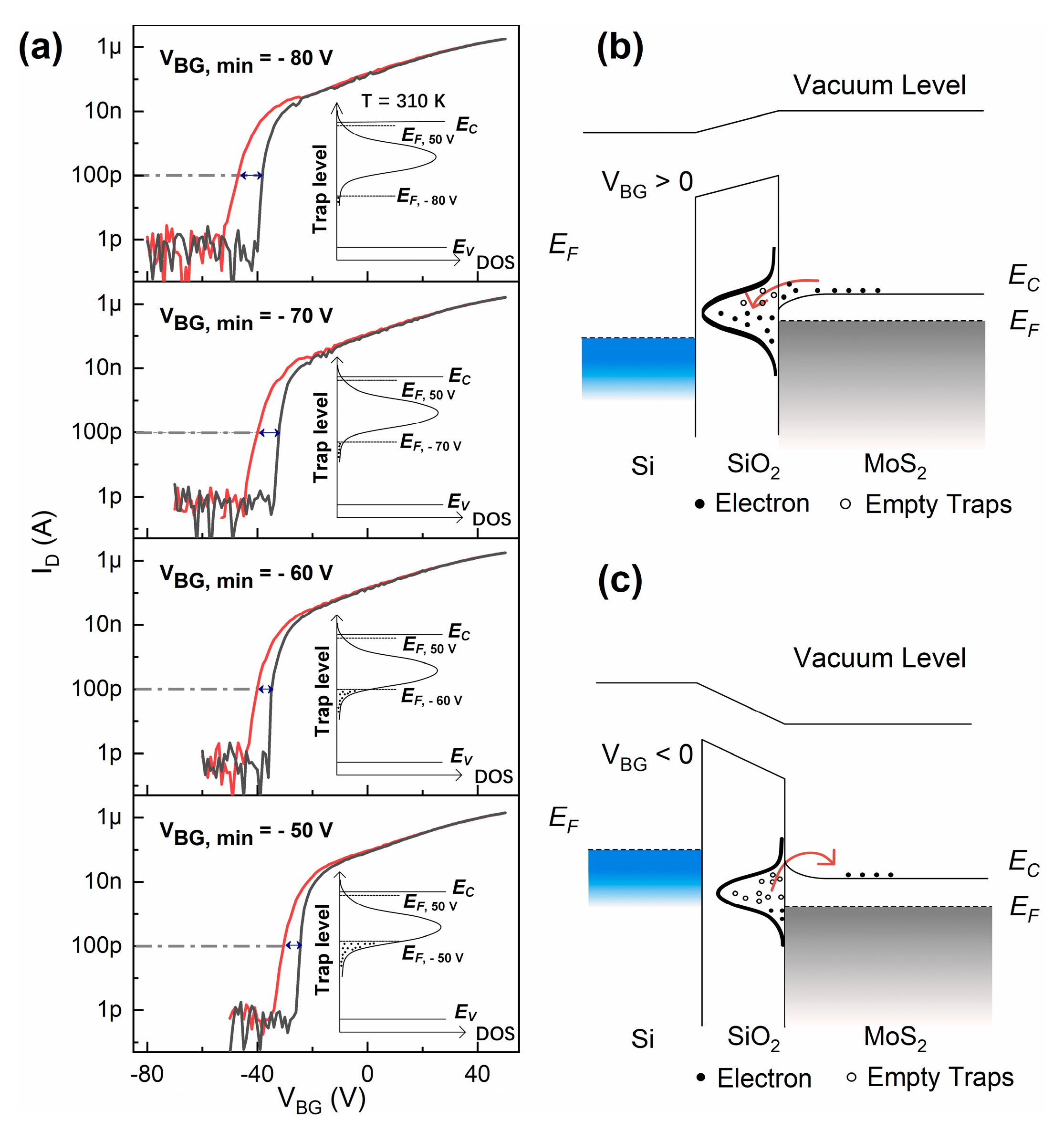
Figure 2a represents the transfer curves of the MoS
2 FET measured at 310 K with varying
VBG, mins. With
VBG, min varied from −50 V to −80 V, the threshold voltage (
VTH) of the device negatively shifted for both forward sweep and backward sweep. For forward sweeps, the threshold voltage of the device shifted from −30 to −43 V. For backward sweeps, the threshold voltage of the device shifted from −23 to −35 V. Meanwhile, the hysteresis of the device increased from 5 to 9 V. For MoS
2 FETs, threshold voltage shift and hysteresis are mainly caused by the interface states acting as charge traps at the MoS
2–SiO
2 interface. These interface states are the result of dangling bonds formed at the surface of SiO
2 during the growth process of SiO
2. By exchanging electrons with the MoS
2 channel, the interface states can be viewed as a “impurity band” in the MoS
2 bandgap [
15,
16]. At 310 K, as the gate voltage sweeps from
VBG, min to 50 V, the conduction band bends downward relative to the Fermi level. The positions of the Fermi level corresponding to
VBG, mins of −50 to −80 V are shown, respectively, in the inset of
Figure 2a. As the gate voltage increases, a part of energy levels of the interface states will be swept over by the Fermi level. This will cause the charge traps to capture/release electrons. When the energy levels of the interface states are below the Fermi level, it indicates the energy level are occupied by electrons as shown in
Figure 2b. When the energy levels of the interface states are above the Fermi level, electrons that used to be trapped in these interface states tend to get de-trapped, as shown in
Figure 2c. When a negative gate bias is applied at the beginning of forward sweep, a portion of electrons are released to the MoS
2 channel, the empty traps become positively charged. This will weaken the depletion of the MoS
2 channel, because the positive charges will partially “screen” the negative gate voltage. The threshold voltage will then negatively shift. For a more negative
VBG, min, more positive charges will be present. Then, it will require a more negative gate bias to depletion the MoS
2 channel. Therefore, the threshold voltage will keep on shifting to the negative direction. As for the hysteresis, because we used a constant gate voltage sweeping rate of 2 V/s, the accumulation time interval in one gate voltage sweep cycle is 50 s. The depletion time interval from
VBG, min to 0 V in the forward sweep is shorter than the accumulation time interval, even for the
VBG, min of −80 V condition. Together with the fact that the de-trapping process is much lower than electron movements in the MoS
2 channel [
8], the refilled traps during the accumulation process will partly screen the negative gate voltage and cause a positive shift of
VTH. Thus, the hysteresis occurs.
Like hysteresis and threshold voltage shift,
SS shift can also be attributed to the interface states. However, the
SS shift can hardly be observed without gate bias stressing [
17], because the density of states (DOS) distribution of interface states is seldom considered. In this study, DOS distribution of the interface states is assumed to coincide with Gaussian distribution and its maximum value is located at a few tens of meV below the conduction band, as shown in
Figure 2 [
15,
18,
19]. For both forward sweeps and backward sweeps, as the gate voltage sweeping range expands, the
SS of the device is enlarged because more traps are depleted or in other words “activated” when larger negative gate bias is used.
SS increases from 2188 to 2898 mV/dec for forward sweeps.
SS increases from 648 to 1550 mV/dec for backward sweeps. For forward sweeps, the interface states density (
Dit) is extracted to be 2.64 × 10
12 eV
−1cm
−2 for
VBG, min of −50 V, and
Dit is extracted to be 3.49 × 10
12 eV
−1cm
−2 for
VBG, min of −80 V, by using the following equations [
20]:
where
k is the Boltzmann’s constant,
T is the measurement temperature,
q is the electron charge, and
Cox is the gate dielectric capacitance density which is 11.5 nF/cm
2 (
Cox =
ɛ0ɛr/d;
ɛr = 3.9;
d = 300 nm) for the MoS
2 FET.
To further study the mechanism of the
SS shift, we conducted transfer characteristics measurements at a series of temperatures.
Figure 3a,b show the transfer curves for
VBG, mins of −50 V for forward and backward sweeps, respectively, in a temperature range from 10 to 310 K. The
VTH shifts negatively as temperature increases. The transfer curves for
VBG, mins from −60 to −80 V in steps of −10 V with constant
VDS = 1 V were also measured. The relationship between
VTH, temperature, and
VBG, min is extracted and illustrated in
Figure 3c,d for forward and backward sweeps, respectively. For more negative
VBG, mins, the
VTH shift enlarges more abruptly compared to less negative
VBG, mins when the temperature is above 100 K, which means the “screening” mentioned above becomes stronger above 100 K. No gate bias stressing is applied in this experiment, therefore the electron exchange between the MoS
2 channel and interface states is incomplete. For more complete delegation by larger gate bias, the “effective”
Dit is higher. As the unoccupied traps are positively charged, the electrons in the MoS
2 channel will suffer from Coulomb scattering. We have
, wherein
the conductance of the MoS
2,
is the coefficient that reflects the screening of Coulomb scattering. If the Coulomb scattering is fully screened, then
. For bare Coulomb scattering,
. As
,
, the coefficient
is the slope of
versus
[
8]. By calculating the data from
Figure 3a,b, we obtain a minimum
of 1.56 for
VBG, min of −80 V and a maximum
of 1.72 for
VBG, min of −50 V at 310 K. The fact that more negative
VBG, min corresponds to weaker Coulomb scattering indicates the extra electrons depleted to the MoS
2 channel by the larger
VBG, m (more negative) is more effective on screening the Coulomb scattering caused by the unoccupied traps than causing more severe scattering. This also suggests large amount of interface states intrinsically exist at the MoS
2/SiO
2 interface.
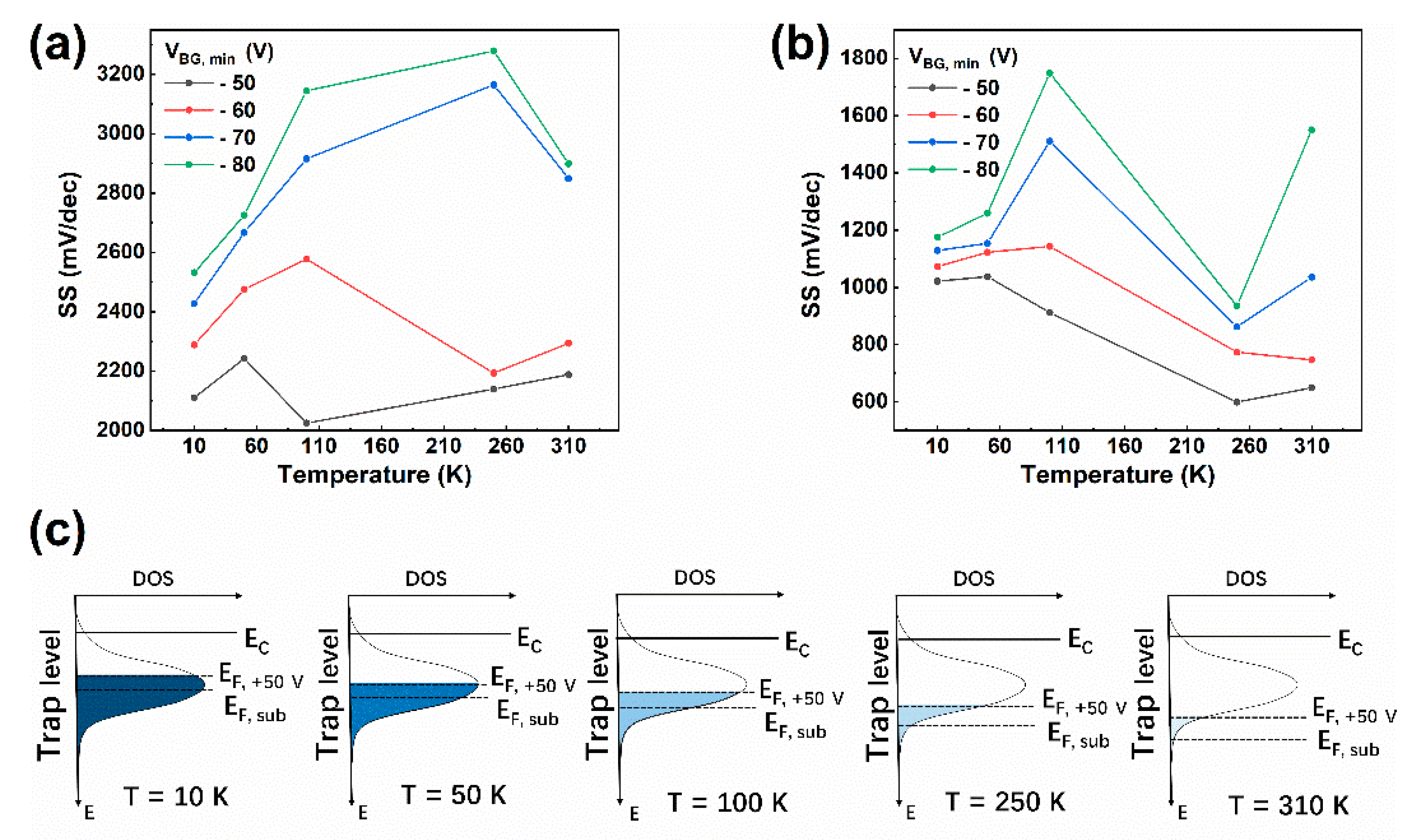
Figure 4a,b show the relationship between
SS and temperature extracted from
Figure 3a,b for forward sweep and backward sweep, respectively. Normally,
SS should have a linear relationship with temperature. However, for forward sweeps, for
VBG, min of −50 V, the
SS versus
T curve increased from 10 K and reached a maximum mV/dec at 50 K, then dropped to a minimum at 100 K, and began to increase linearly above 100 K. The
SS versus temperature curve presents an abnormal bulge in the temperature range of 10 to 100 K. For
VBG, min of −60 V, the bulge expands to 250 K and
SS begins to increase linearly from there on. As
VBG, min further decreases to −70 V, the bulge expands at least to 310 K. For
VBG, min of −80 V, the range of the bulge is similar to that for
VBG, min of −70 V. Although for
VBG, mins of −70 and −80 V, the
SS does not show a linear increase in the temperature range of this experiment; we believe the
SS will still begin to increase linearly at a higher temperature. For backward sweeps, the range of the bulge is almost the same for each
VBG, min. The
SS curves all begin to increase linearly at around 250 K. Moreover, the scale of the bulge is even larger for small
VBG, mins compared to forward sweeps. For this abnormal deviation of
SS from linearity with temperature, the energetic distribution of interface states density and the temperature induced Fermi level shift mechanisms are adopted to explain it.
Due to the trapping and releasing processes of electrons in the traps, the interface states can be viewed as a capacitor. The capacitance
Cit is determined by the density of the interface states
Dit. Thus,
Dit is the key to study this abnormal relationship between
SS and temperature. As we assume
Dit has Gaussian distribution as shown
Figure 2, it can be written as
and
f (
E) in Equation (3) can be written as
where in
Dit, max (
E) is the maximum value the
Dit can reach during the shift of Fermi level as temperature increases,
EF (
T) is the location of Fermi level as a function of temperature, and
f (
E) is the energetic distribution function of the interface states [
19,
21].
f (
E) represents the possibility that a certain energy level is occupied.
FWHM is the full width at half maximum of
Dit. On the other hand, because of the activation of bulk charge traps (including bulk MoS
2 trap charges, fixed oxide charges, and oxide trap charges inside a thick SiO
2 insulator) and interface states [
22], the location of the Fermi level can be modulated by temperature and can be expressed as
corresponding to low temperature weak ionization region (Equation (5)) and high temperature strong ionization region (Equation (6)), wherein
EC,
NC, and
ND are the bottom of the conduction band, effective density of states of conduction band, and donor concentration of the interface states for MoS
2, respectively. As shown in
Figure 4c, the position of the Fermi level corresponding to subthreshold situation (
EF, sub) shifts downward relative to the energy levels of the interface states when temperature increases from 10 to 310 K. Thus, the
Dit corresponding to
EF, sub will change with temperature.
Due to the Gaussian distribution,
Dit has a maximum value
Dit, max. For a certain temperature, the more the Fermi level approaches
Dit, max, the larger the
SS is and vice versa. When substituting above Equations (2)–(6) back into Equation (1), the expression of
SS can be written as
The deduced expression for
SS has two terms. The first term is a nonlinear term which corresponds to the depletion of interface states by the gate voltage, and the second term is a linear term which is only affected by temperature. Taking the situation for
VBG, min of −50 V as an example, for forward sweep, from 10 to 50 K,
Dit corresponding to
EF, sub increases rapidly. Thus, the nonlinear term of Equation (7) dominates and the
SS curve begins to increase and deviate from linearity. After 50 K, as
EF, sub passed
Dit, max, the nonlinear term begins to decrease. If the increasing of the linear term and the decreasing the nonlinear term reach an equilibrium, the
SS will saturate. When temperature continues to increase, the drop down of
Dit will experience an acceleration. The nonlinear term will dominate again during this fast drop and
SS will drop with it. When the decrease of
Dit slows down at a position that is far from
Dit, max, another equilibrium with the linear term will be accomplished. Thus,
SS will reach a minimum. As the temperature further increases, the linear term will dominate and the nonlinear term will be negligible. The
SS will increase linearly along with the linear term. When
EF, sub shifts downward as temperature increases, because the effective
Dit is actually higher compared to the situation for
VBG, min of −50 V, the
SS will be generally larger, as can be seen in
Figure 4a,b and the shift of
EF, sub will be slowed down in the temperature dimension because more traps have to be thermally activated. Then the maximum or minimum of
SS will be achieved at higher temperatures. The above discussion also explained why the deviation from linearity is hardly observed for small gate voltage sweep ranges (e.g., from −30 V to 30 V) in which case the effect of the nonlinear term is too small and is covered up by the linear term. For backward sweep, because the traps refilled when the gate voltage is positive have not fully de-trapped yet. Then, effective
Dit becomes smaller compared to forward sweep. The
SS for backward sweep is thus generally smaller than that for forward sweep. This result coincides with the fact that the
VTH shift for backward sweep is generally smaller than that for forward sweep, which also originates from the more incomplete depletion of interface states for backward sweep. From the above discussion, we can infer that the
FWHM of
Dit is important for whether the deviation of
SS from linearity can be observed. If the
FWHM is small enough, the distribution of
Dit can be viewed as a step function. The slope of
SS will change abruptly to another value at a certain temperature as is observed by Park et al. [
22,
23]. However, if the
FWHM is large, the situation will become what we observed for our MoS
2 FET.

 ,
, 