Article

Deposition of Thin Alumina Films Containing 3D Ordered Network of Nanopores on Porous Substrates

1
Ruđer Bošković Institute, Division of Materials Physics, Bijenička cesta 54, 10000 Zagreb, Croatia
2
Laboratory of Nanoscale Biology, Institute of Bioengineering, School of Engineering, EPFL, 1015 Lausanne, Switzerland
3
National Institute of Chemistry, Hajdrihova 19, 1001 Ljubljana, Slovenia
4
Elettra-Sincrotrone Trieste, 34149 Basovizza, Italy
5
Institute of Physics, Bijenička Cesta 46, 10000 Zagreb, Croatia
*
Author to whom correspondence should be addressed.
Materials 2020, 13(13), 2883; https://doi.org/10.3390/ma13132883
Submission received: 18 May 2020 / Revised: 11 June 2020 / Accepted: 22 June 2020 / Published: 27 June 2020

Abstract

:
Self-supporting thin films containing nanopores are very promising materials for use for multiple applications, especially in nanofiltration. Here, we present a method for the production of nanomembranes containing a 3D ordered network of nanopores in an alumina matrix, with a diameter of about 1 nm and a body centered tetragonal structure of the network nodes. The material is produced by the magnetron sputtering deposition of a 3D ordered network of Ge nanowires in an alumina matrix, followed by a specific annealing process resulting in the evaporation of Ge. We demonstrate that the films can be easily grown on commercially available alumina substrates containing larger pores with diameters between 20 and 400 nm. We have determined the minimal film thickness needed to entirely cover the larger pores. We believe that these films have the potential for applications in the fields of filtration, separation and sensing.

Graphical Abstract

1. Introduction

Nanoporous thin films are widely used for various applications such as energy conversion and storage [1,2,3,4], the selective separation of molecules [5,6,7] and filtration [8,9,10]. Commercially available nanoporous membranes generally exhibit broad size distributions and relatively large thickness. As a result, the materials usually possess poor size-cutoff properties and low transport rates. A separation of similarly sized materials with current commercially available nanoporous membranes is not feasible. Depending on the desired application, the fabrication of membranes with a very small size can be desirable. For instance, in hydrogen separation, the maximum pore size is between 0.3 nm and 0.4 nm [4,11], while for CO2 separation, the pore sizes range from 0.3 nm to 1.3 nm [12]. In water desalination, the pore size has a key role in governing the movement of water through the membrane. The diameter of the water molecular cluster is between 0.5 and 0.65 nm while the pore diameters of hydrated Na+ and Cl ions are 0.64 and 0.77 nm, respectively [13,14]. Another very interesting application of ultrathin nanoporous membranes is the conversion of the Gibbs free energy stored in salinity gradients to electricity [15]. Yan, Fei, et al. fabricated an ultrathin silica membrane with a pore diameter in a range between 2 and 3 nm for osmotic energy harnessing [16].
Membrane technology has become a promising industrial alternative compared with traditional treatment techniques, such as distillation, absorption, adsorption, extraction, activated sludge and trickling filters. The separation mechanism is principally based on the size exclusion of matter, i.e., substances with sizes larger than the pores of the membranes are rejected. In order to achieve a high selectivity, the pores in a membrane need to be smaller than the particles in the mixture that we want to separate. The chemical and thermal stabilities are very important to consider when selecting the materials for membranes. For example, polymeric membranes cannot withstand many organic solvents or high-temperature conditions. In these hard conditions, inorganic membranes are usually more suitable. Alumina is a very good material for porous membranes because it is chemically stable, semitransparent, insoluble, inert, and biocompatible [17,18,19]. One of the very attractive applications of nanoporous alumina membranes is their incorporation into a wide variety of sensors [20,21,22,23], for filtration purposes [8,17,24,25] and water treatment [26,27,28,29,30,31].
Many efforts have been made to find a method that would allow the synthesis of uniform, self-supporting alumina membranes with pores in the nano-range. A detailed overview of the preparation of anodic aluminum oxide was given in [32]. During this process, a self-organized, highly ordered array of cylindrically shaped pores is usually produced with a controllable pore diameter. These films are usually prepared by the anodization of aluminum in an appropriate acidic or alkaline solution. With this method, it is possible to fabricate pores whose diameter is as small as 12 nm. The preparation of porous material using organic surfactant molecules is discussed in more detail in [33]. Liu, Yang and coworkers prepared highly permeable alumina membranes by the UV curable technique. The network is formed by the cross-linking of photo curable resins that resulted in rapid solidification of the wet membrane. The most frequent pore size for membranes prepared with this technique was 65.2 nm [34].
Germanium oxidation has been widely investigated in the field of surface science. GeO evaporation is promoted by increasing temperature, since a higher temperature results in a higher vacancy flux toward the surface [35]. The interface reaction is as follows: GeO2 + Ge→2GeO [36,37,38]. In our previous work, we have shown that the annealing of regularly ordered inter-connected Ge quantum dot (QD) lattices can result in the formation of regularly ordered void lattices in an Al2O3 matrix by Ge oxidation [21,22]. The complete desorption of Ge was confirmed using Rutherford backscattering spectrometry measurements. The structural properties of the pores including their size and arrangement, were investigated using grazing incidence small angle x-ray scattering (GISAXS). These measurements confirmed that the structure after annealing is the same as it was before it [39]. In other work, the annealing conditions leading to the formation of a void lattice have been investigated [40]. It was found that complete Ge desorption takes place for a critical annealing air atmosphere pressure of 10−3 Pa. For high vacuum annealing conditions, there are not enough oxidants present in the annealing atmosphere for the formation of a GeO2 layer, so the Ge loss process from the film is inhibited. The oxidation of Ge QDs in an alumina matrix was already investigated [41]. It was found that Ge QDs in an Al2O3 matrix are oxidized in large amounts because they are very sensitive to the presence of any oxygen in the deposition chamber.
In this paper, we present a simple method for the fabrication of nanoporous alumina membranes, with a regular arrangement of the pores in a 3D network, having a small pore diameter (~1 nm), and thicknesses of up to 100 nm. The membranes are grown by the magnetron sputtering deposition of thin Ge + Al2O3 film on commercially available porous alumina membrane with large pore sizes (20–400 nm), followed by specific annealing. In the produced films, the nanopores are arranged in a 3D-ordered continuous network with the arrangement of the nodes controllable by the deposition conditions. The mechanism of thin-film growth over the larger substrate pores is investigated, and a method of reducing the large pore size to the desired value is demonstrated. The presented nanomembranes are interesting for applications in filtering, separation and sensing.

2. Materials and Methods

2.1. Preparation Parameters

The materials were produced by co-deposition from Ge (99.999%) and Al2O3 (99.999%) targets using the magnetron sputtering KJLC CMS-18 system. The thin Ge+Al2O3 films were simultaneously deposited on three different substrates: quartz, Si (100) substrates, and porous Anodic aluminum oxide (AAO) membranes (Anopore), produced by Whatman (Whatman® Anodisc Inorganic Membranes, provided by Sigma-Aldrich Chemie GmbH, Germany, diameter 47 mm). In the latter case, the films were deposited either on the side of the membrane with smaller pores (20–40 nm) or on the other side having larger pores (about 200 nm). The aim was to cover the AAO membrane with a thin nanoporous alumina film, as illustrated in Figure 1a. Additionally, one film was deposited over the opening of the initial diameter of ~220 nm, in a 20 nm thin SiNx membrane. The membrane was etched in silicon substrate by photolithography, followed by dry and wet etching. The opening was then created by focused ion-beam drilling (FIB). The process was previously published in Feng et al. [42]. The films were prepared on different substrates to allow the use of different characterization techniques.
The substrates were cleaned with acetone, isopropyl alcohol and deionized water in an ultrasound bath before loading into the deposition chamber.
For the deposition of Ge and Al2O3, we used Direct Current (DC) and Radio Frequency (RF) magnetrons, respectively. The Ge sputtering power was tuned from 3 W to 13 W, while the power of the Al2O3 sputtering was kept constant at 140 W. The argon pressure was 3.5 Torr for all the films, and the deposition temperature was 300 °C. The deposition parameters for all the films are given in Table 1. Two series of films were deposited, differing by the Ge sputtering power (denoted by letter P) and by the deposition time (denoted by letter D). Thus, the name of each film consists of two letters denoting the deposition time and Ge power (for example, P1D1), as shown in Table 1. Additional films having the same sputtering powers and longer deposition times were prepared for some of the measurements to ensure better statistics.
After the deposition, the films consisted of a 3D mesh of Ge nanowires embedded in an Al2O3 matrix. In order to achieve Ge evaporation, a heat treatment was performed in a low vacuum (10−2 mbar) environment in an electric furnace for lab heat treatment. After the thermal annealing for 4 min at 630 °C, the Ge was removed from the sample leaving the porous structure behind. The color of the films on quartz substrate and AAO membrane changed during the annealing from brown, which is caused by the Ge presence, to transparent after the Ge evaporation, as visible from Figure 1b. In order to be able to clearly distinguish the films and substrates, we use the following notations: (i) Ge-based film for the as-deposited, non-porous film; (ii) nanoporous film for the annealed Ge-based film, which has nanopores that we use to cover the substrate pores; and (iii) AAO substrate membrane for the anodic alumina with the large pores.

2.2. Characterization Techniques

The grazing incidence small-angle x-ray scattering (GISAXS) measurements were performed at the synchrotron Elettra, Trieste, Italy at the SAXS beamline using a photon energy of 8 keV and a Pilatus3 1M detector. The films deposited on non-porous Si substrates were used only for the GISAXS measurements. We expect the same structure of the films grown on membranes and SiNx membrane because they grow with the same mechanism independently on the substrate. The GISAXS maps were numerically analyzed using the procedure described in [43,44,45].
The transmission electron microscopy (TEM) of the cross-section of the film was performed using a JEOL ARM 200 CF scanning transmission electron microscope (STEM), operated at 200 kV and equipped with a field-emission gun and a high-angle annular dark-field detector (HAADF) for Z-contrast imaging.The TEM of the opening in the SiNx membrane overgrown by the film was performed using Talos TEM (ThermoFisher Scientific, Hillsboro, OR, USA) at 200 kV.
The scanning electron microscopy (SEM) was performed using the thermal field emission scanning electron microscope (FE SEM, model JSM-7000 F) manufactured by JEOL Ltd (Tokyo, Japan). FE SEM was linked to the EDS/INCA 350 (energy-dispersive X-ray analyzer) manufactured by Oxford Instruments Ltd. (Abingdon, UK).

3. Results

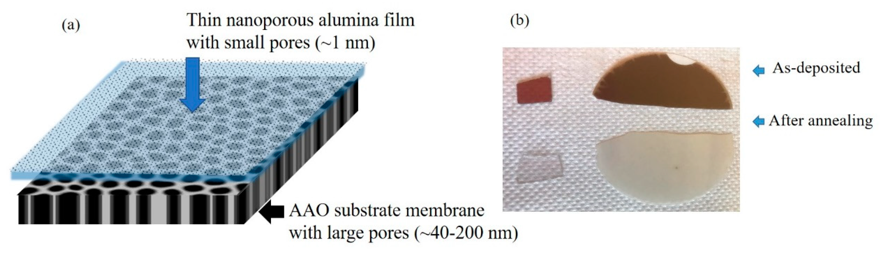
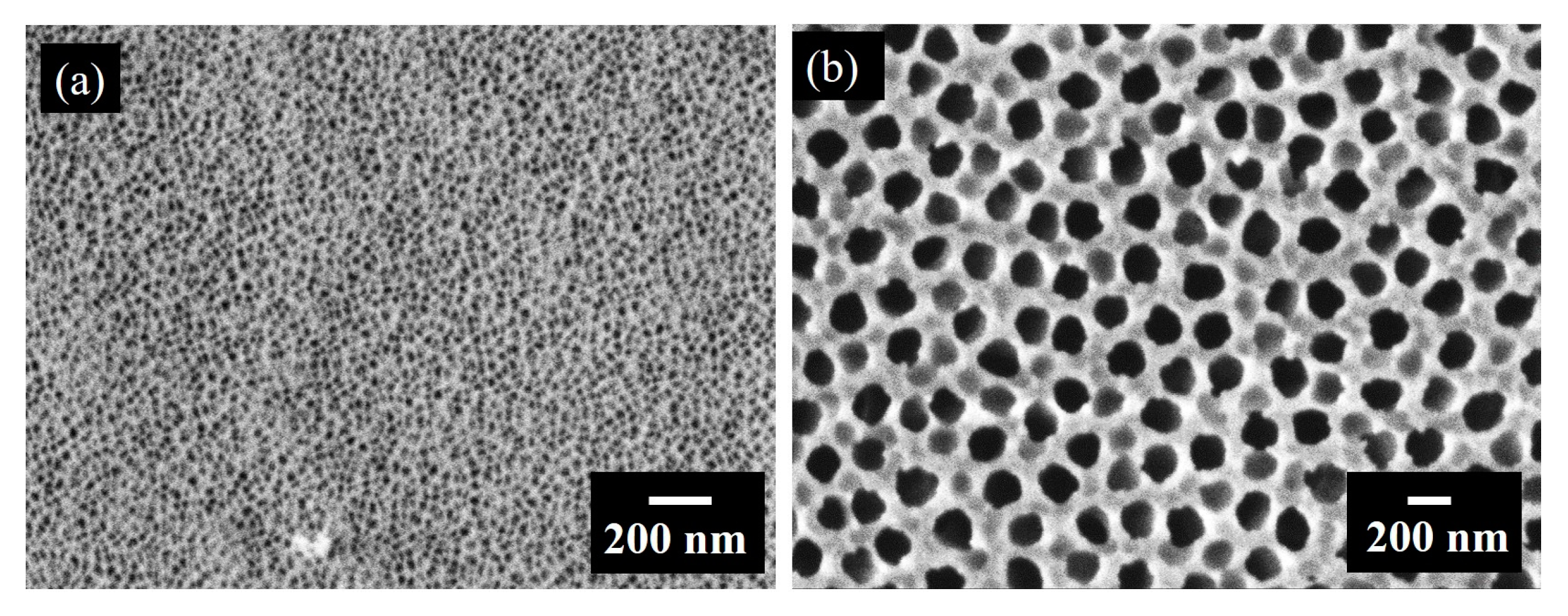
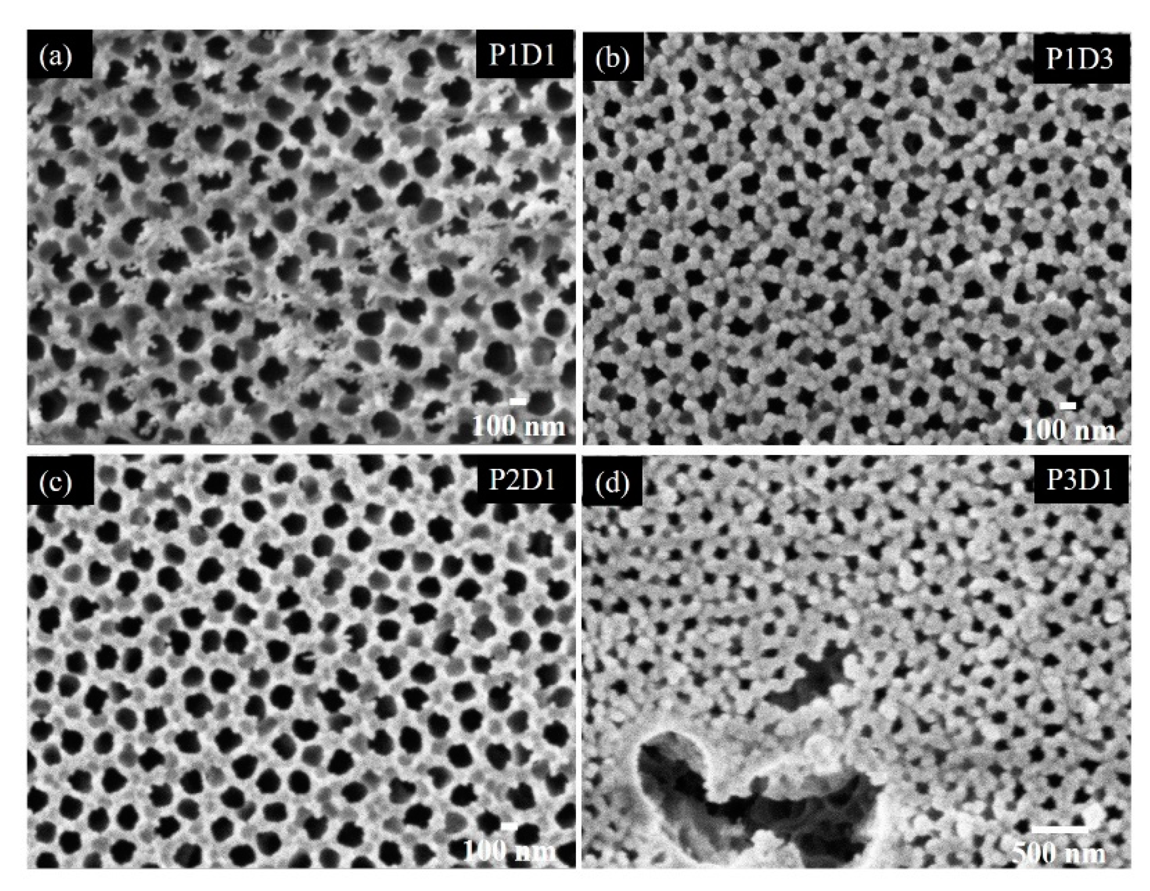
3.1. Structural Properties of Thin Nanoporous Films

In this section, we analyze the nanostructure of the films itself. In the next section, we investigate how they cover the substrate having larger pores.
The typical structural properties of the prepared films are demonstrated in Figure 2. The model of an ideal network structure is shown in Figure 2a, while the main parameters of it are illustrated in Figure 2b. The nanopores make a 3D network having a body centered (BCT) tetragonal arrangement of the nodes. The separation between the nodes in the plane parallel to the substrate is described by the parameter a, while the vertical separation is c. The pores have the radius R and the length L. The TEM images of the film structure are shown in Figure 2c,d. The shown films differ by the Ge sputtering power, resulting in the formation of longer, more separated pores for the smaller Ge power. The networks are continuous, which is ensured by the preparation method, i.e., the evaporation of Ge from the film during the sample annealing. The insertion of even a very thin (1 nm) layer of pure matrix prevents Ge oxide evaporation, because the network is not continuous in that case. Therefore, the same preparation method is not efficient for Ge quantum dot multilayer films. In such films, Ge quantum dots are fully surrounded by alumina matrix, which prevents the evaporation of Ge. Therefore, these films cannot be used for the creation of nanoporous films. The GISAXS intensity patterns of the films’ structure are shown in Figure 2e,f. The two characteristic lateral peaks are related to the arrangement of the network nodes and to their regularity. A more regular network produces stronger and narrower Bragg peaks, so the P1D3 film has a better ordering in this case. More details about the GISAXS maps of such structures are given in [43,44,45]. GISAXS is very suitable for the analysis of these structures, as it provides data about nanopore ordering and size properties with excellent statistics.
The GISAXS maps of all the investigated films before and after annealing (i.e., with Ge quantum wires and nanopores, respectively) are given in Figure 3. The first three films (Figure 3a–c) differ only by the film thickness (D1–D3), while the last two (Figure 3d,e) have different Ge sputtering powers (P2, P3), i.e., different pore arrangements and size properties. The side maxima in the GISAXS maps (Bragg spots) are at nearly the same positions for the first three films, showing the homogeneity of the structure, because these films differ only by their thickness. For the last two films, the spots become more elongated and more spaced, showing an increase in the disorder and a decrease in the lattice parameters of the formed 3D pore network.
All the films except the last one have nearly the same position of the Bragg spots before and after annealing (first and second rows in Figure 3, respectively), showing that during annealing, the Ge left the film, leaving empty space behind without affecting the alumina. The GISAXS method is sensitive to the electron density contrast between the nano-objects and the matrix. The Ge and alumina have a strong difference in electron density, as well as in the empty space (pores) and alumina. Therefore, we see nearly the same GISAXS maps from the Ge nanowires as from the pores of the same shape in the alumina matrix. Only the last film changed the structure during annealing, probably due to the high percentage of Ge that caused a collapse of the structure after leaving the film. This follows clearly from the GISAXS maps of that film (P3D1, shown in Figure 3c). The GISAXS map of the annealed film (P3D1 annealed) differs significantly from the map of the as-grown film. This fact shows clear evidence that the internal structure changed significantly during annealing. The lateral peaks called Bragg spots are clearly visible in the As-grown film, while they are absent for the annealed one, showing that there is no regular ordering of the pores after annealing.
The GISAXS maps were numerically analyzed using the procedure described in [44,45] in order to obtain the values of the structural parameters of the pores and their arrangement. The results of the analysis are given in Table 2. From the results, we can see that the nanopore radius (R) is around 0.6 nm for all the films. This is due to the same deposition temperature for all the films, as shown in the case of Ge quantum wires in [46]. The deposition time (D1–D3) only significantly influences the thickness of the films (D), assuming a constant Ge sputtering power (P1), while the pore length (L) depends on the Ge sputtering power during the film preparation (P1–P3). The pore length decreases with increasing Ge sputtering power. We want to point out here that the pore length L refers to the length of the pore between the two adjacent nodes of the BCT lattice (please see Figure 2b), but the pores are interconnected, so the real pore length is much larger. The pore length L is not correlated to the film thickness. The film grows homogeneously with the same value of the pore length. More information about the production of Ge quantum wire lattices with different structural parameters is given in [46].
In summary, the structural properties of the nanopores are determined by the properties of the Ge quantum wire lattices. By tuning the deposition parameters, it is possible to produce networks of nanopores having different radii and lengths.

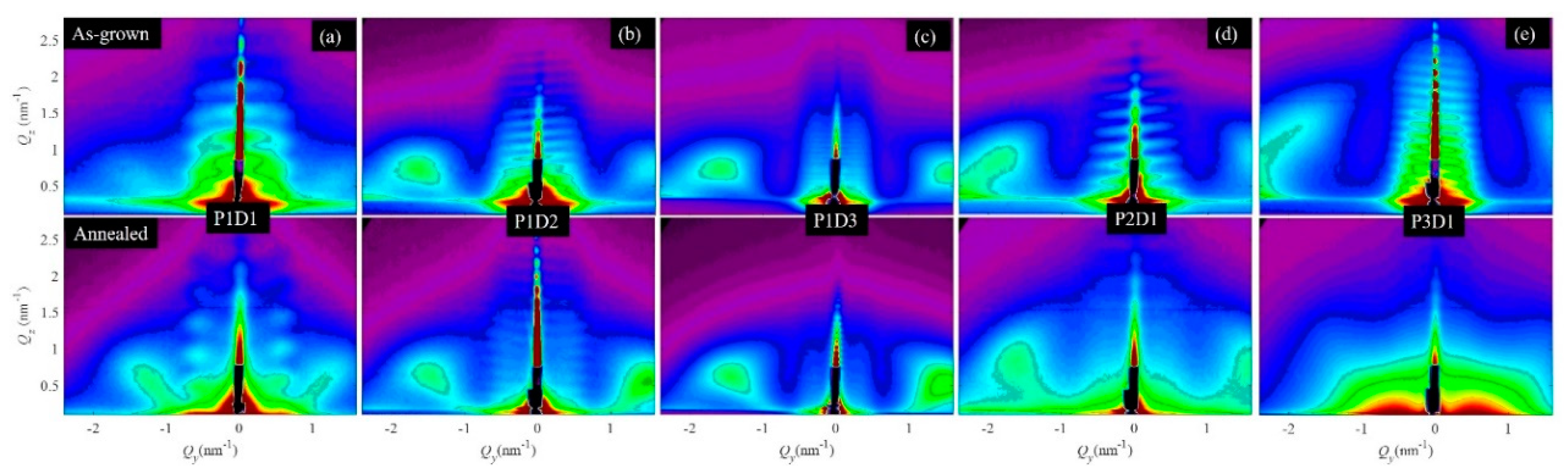
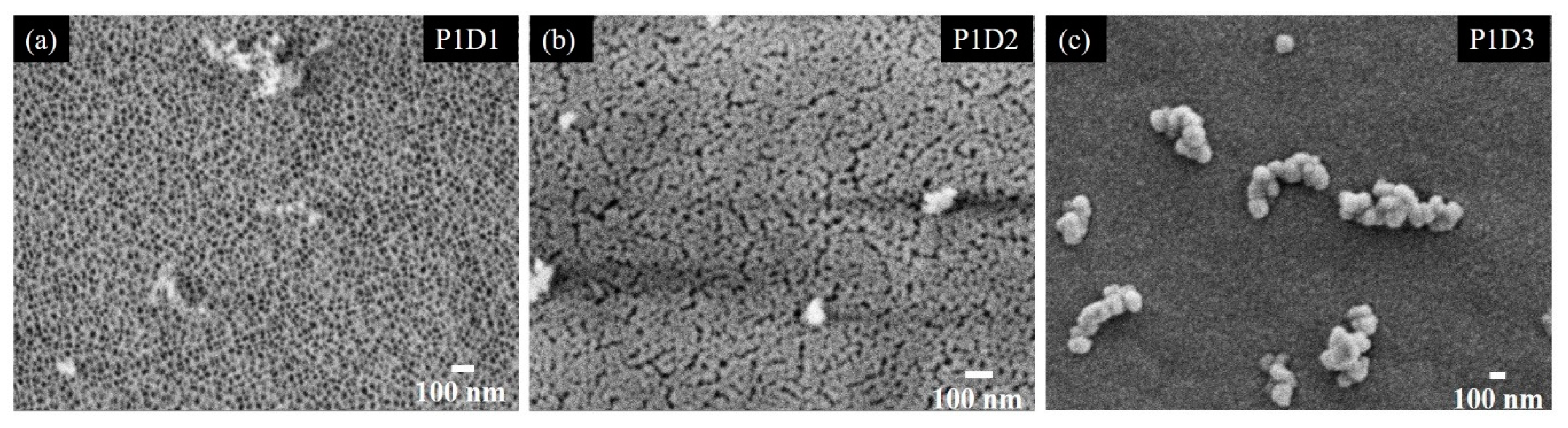
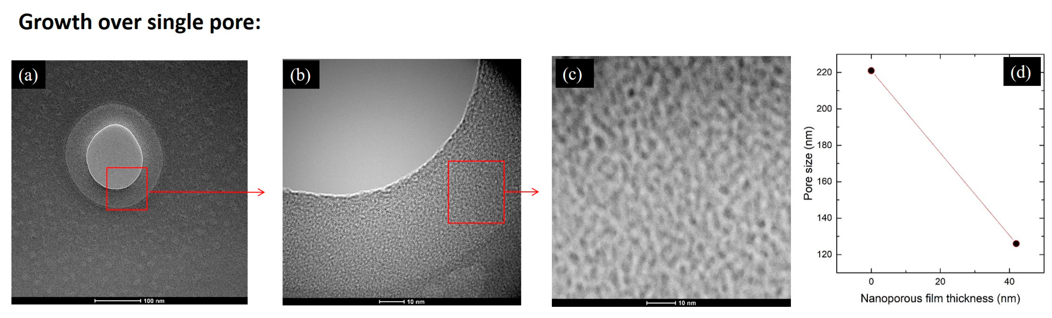
3.2. Growth of Nanoporous Thin Films on Alumina Substrate with Larger Pores

In this section, we investigate the preparation of nanomembranes using the above-mentioned films. As described in the Methods section, we deposited the films on porous alumina substrates (Whatman® Anodisc Inorganic Membranes) having larger pores. The used substrate membranes have different pore sizes on their sides as visible from the SEM measurements, shown in Figure 4. Side 1 has pores with a diameter of 20–40 nm (Figure 4a), and Side 2 has larger pores with a diameter of about 200 nm (Figure 4b).
The effect of the film deposition on Side 1 of the membrane is shown in Figure 5. The SEM images of the film’s surface clearly show the coverage of the pores with increasing film thickness D. The thinnest film P1D1 shown in Figure 5a does not cover the pores. The coverage is complete for the middle thickness (40 nm) shown in Figure 5b. This indicates that the minimal film thickness needed to achieve the full coverage of the substrate holes is found to be nearly equal to the lateral size of the holes. However, features similar to cracks are visible in the film structure. A complete coverage and a smooth film surface are achieved for the film P1D3 having the largest thickness of about 80 nm.
The coverage of the larger pores (Side 2) of the AAO substrate by the films is shown in Figure 6. The films differing by the deposition time are shown in Figure 6a,b, and the films differing by Ge sputtering power are shown in Figure 6c,d. The pores are not fully covered in all cases; however, the pore sizes are strongly reduced for the longest deposition time (P1D3) and for the largest Ge sputtering power (P3D1). Since the reduction of the pore size is proportional to the film thickness, this technique can be applied for tailoring the pore size to desired value.
The effect of the pore coverage is also investigated on a single opening (pore) in the SiNx membrane; see Figure 7. The single opening of initial diameter of ~220 nm was investigated by TEM to inspect the overgrowth behavior of the films on different substrates. Figure 7a shows the opening having a diameter of ~120 nm after the growth of the film P3D1 with the thickness of 42 nm. The non-covered part of the opening is visible as a circular shape in light-gray color. The grown film appears slightly darker, while the rest of the membrane exhibits a dark gray color. The effect is better visible in Figure 7b where the enlarged part of the opening is shown. The nanopores in the film are visible, and the thickness of the covered part of the opening is about 40 nm. As visible from the images, the film narrowed the opening for the value of its thickness, shrinking the pore down to ~120 nm. The nanoporous structure of the film is shown in Figure 7c. Results for the reduction of the pore size in the SiNx membrane shown in Figure 7a–c, are shown in Figure 7d. The curve shows a negative slope with the value of 2.26, which may be used for the estimation of the pore size reduction using the presented technique.

4. Conclusions

We have demonstrated a simple method to produce self-supporting alumina nanomembranes with a 3D-ordered network of nanopores having a body-centered tetragonal ordering of its nodes and a pore diameter of about 1 nm. The membranes are produced by the magnetron sputtering deposition of thin films consisting of a 3D network of Ge quantum wires in an alumina matrix. The films are deposited on a large-pore alumina substrate, followed by a specific annealing process. The annealing induces Ge evaporation, resulting in the formation of a 3D network of nanopores. The film covers the larger pores, and the minimal film thickness needed to achieve the full coverage of the substrate holes is nearly equal to half of the lateral hole size. However, thicker films ensure defect-free pore coverages. This method can also be used for reducing larger pore sizes to a desired value. The pore sizes and inter-pore distance can be controlled by the deposition conditions. We believe that these nanomembranes could be used for sensing applications and filtration and separation purposes. Additionally, the same material can be produced using other volatile elements instead of Ge, and that will be the topic of our future work.

Author Contributions

Conceptualization, M.M. and M.T.; methodology, M.M. and M.T.; software, M.M.; validation, L.B., M.T. and M.M.; formal analysis, L.B., M.T. and M.M.; data curation, L.B., M.M. and M.T.; writing—original draft preparation, M.T. and M.M.; GISAXS measurements and analysis, S.B., M.T. and L.B.; STEM measurements, G.D.; SiNx membrane preparation and TEM measurements, M.L. and T.V.; SEM measurements, M.G.; writing—review and editing, M.T., M.G., L.B., M.L., G.D., S.B., T.V. and M.M.; visualization, M.M.; supervision, M.M.; project administration, M.M.; funding acquisition, M.M. All authors have read and agreed to the published version of the manuscript.

Funding

This research was funded by the Croatian Science Foundation (No. IP-2018-01-3633) and the Center of Excellence for Advanced Materials and Sensing Devices (Grant KK.01.1.1.01.0001). This work was supported by the CalipsoPlus project (pr. no 20177127). M.L. and T.V. acknowledge the Unity through Knowledge Fund, Croatia grant no. 17/13.

Acknowledgments

The authors are thankful to Joško Erceg for the assistance in the sample preparation and Dario Mičetić for GISAXS measurements. M.L. and T.V. thank Aleksandra Radenovic from École polytechnique fédérale de Lausanne (EPFL, Switzerland) for their collaboration, the Center for Micro/Nanotechnology (CMi, EPFL), and the Centre Interdisciplinaire de Microscopie Electronique (CIME) at EPFL for access to electron microscopes.

Conflicts of Interest

The authors declare no conflict of interest. The funders had no role in the design of the study; in the collection, analyses, or interpretation of data; in the writing of the manuscript, or in the decision to publish the results.

References

  1. Chen, Z.; Zhao, X.; Tang, Y. Thin Films for Energy Harvesting, Conversion, and Storage; Multidisciplinary Digital Publishing Institute: Basel, Switzerland, 2019; Volume 9, ISBN 9783039217243. [Google Scholar]
  2. Yang, Y.; Fan, X.; Casillas, G.; Peng, Z.; Ruan, G.; Wang, G. Three-Dimensional Nanoporous Thin Films for Lithium-Ion Batteries. ACS Nano 2015, 8, 3939–3946. [Google Scholar] [CrossRef]
  3. Перспективный, В.; Для, М.; Энергетики, В. Nanocrystalline porous vn x hydrogen storage as the promising material for hydrogen energy. Mach. Technol. Mater. 2016, 2, 75–77. [Google Scholar]
  4. Veronica Sofianos, M.; Sheppard, D.A.; Ianni, E.; Humphries, T.D.; Rowles, M.R.; Liu, S.; Buckley, C.E. Novel synthesis of porous aluminium and its application in hydrogen storage. J. Alloy. Compd. 2017, 702, 309–317. [Google Scholar] [CrossRef] [Green Version]
  5. Li, B.; Japip, S.; Chung, T.S. Molecularly tunable thin-film nanocomposite membranes with enhanced molecular sieving for organic solvent forward osmosis. Nat. Commun. 2020, 11, 1–10. [Google Scholar] [CrossRef] [PubMed] [Green Version]
  6. Sano, T.; Iguchi, N.; Iida, K.; Sakamoto, T.; Baba, M.; Kawaura, H. Size-exclusion chromatography using self-organized nanopores in anodic porous alumina. Appl. Phys. Lett. 2003, 83, 4438–4440. [Google Scholar] [CrossRef]
  7. Qiu, X.Y.; Yu, H.Z.; Peinemann, K.V. Selective separation of similarly sized proteins with tunable nanoporous block copolymer membranes. Procedia Eng. 2012, 44, 461–463. [Google Scholar] [CrossRef] [Green Version]
  8. Osmanbeyoglu, H.U.; Hur, T.B.; Kim, H.K. Thin alumina nanoporous membranes for similar size biomolecule separation. J. Memb. Sci. 2009, 343, 1–6. [Google Scholar] [CrossRef]
  9. Nehache, S.; Semsarilar, M.; Deratani, A.; Quemener, D. Negatively charged porous thin film from ABA triblock copolymer assembly. Polymers 2018, 10, 733. [Google Scholar] [CrossRef] [PubMed] [Green Version]
  10. Wang, Z.; Wu, A.; Ciacchi, L.C.; Wei, G. Recent advances in Nanoporous Membranes for Water Purification. Nanomaterials 2018, 8, 65. [Google Scholar] [CrossRef] [Green Version]
  11. Dong, J.; Lin, Y.S.; Kanezashi, M.; Tang, Z. Microporous inorganic membranes for high temperature hydrogen purification. J. Appl. Phys. 2008, 104, 13. [Google Scholar] [CrossRef]
  12. Korelskiy, D.; Grahn, M.; Ye, P.; Zhou, M.; Hedlund, J. A study of CO2/CO separation by sub-micron b-oriented MFI membranes. RSC Adv. 2016, 6, 65475–65482. [Google Scholar] [CrossRef] [Green Version]
  13. Heiranian, M.; Farimani, A.B.; Aluru, N.R. Water desalination with a single-layer MoS 2 nanopore. Nat. Commun. 2015, 6, 1–6. [Google Scholar] [CrossRef] [PubMed] [Green Version]
  14. Wang, Y.; He, Z.; Gupta, K.M.; Shi, Q.; Lu, R. Molecular dynamics study on water desalination through functionalized nanoporous graphene. Carbon N. Y. 2017, 116, 120–127. [Google Scholar] [CrossRef]
  15. Macha, M.; Marion, S.; Nandigana, V.V.R.; Radenovic, A. 2D materials as an emerging platform for nanopore-based power generation. Nat. Rev. Mater. 2019, 4, 588–605. [Google Scholar] [CrossRef]
  16. Yan, F.; Yao, L.; Chen, K.; Yang, Q.; Su, B. An ultrathin and highly porous silica nanochannel membrane: Toward highly efficient salinity energy conversion. J. Mater. Chem. A 2019, 7, 2385–2391. [Google Scholar] [CrossRef]
  17. Smilek, J.; Kynclová, H.; Sedláček, P.; Prášek, J.; Klučáková, M. Specific permeability of nanoporous alumina membranes studied by diffusion cell technique. In Proceedings of the Nanocon 2015-7th Int. Conf. Nanomater.-Res. Appl. Conf. Proc., Brno, Czech Republic, 14–16 October 2015; pp. 348–353. [Google Scholar]
  18. Brüggemann, D. Nanoporous aluminium oxide membranes as cell interfaces. J. Nanomater. 2013, 2013, 18. [Google Scholar] [CrossRef]
  19. Bragazzi, N.L.; Gasparini, R.; Amicizia, D.; Panatto, D.; Larosa, C. Porous Alumina as a Promising Biomaterial for Public Health, 1st ed.; Elsevier Inc.: Amsterdam, The Netherlands, 2015; Volume 101. [Google Scholar]
  20. Yamaguchi, A.; Hotta, K.; Teramae, N. Optical waveguide sensor based on a porous anodic alumina/aluminum multilayer film. Anal. Chem. 2009, 81, 105–111. [Google Scholar] [CrossRef]
  21. Sciuto, A.; Mazzillo, M.C.; Di Franco, S.; Mannino, G.; Badala, P.; Renna, L.; Caruso, C.; Korotcenkov, G.; Cho, B.K.; Zargar, Z.H.; et al. Alcohol sensor based on gold-coated nanoporous anodic alumina membrane. Anal. Chim. Acta 2019, 81, 105–111. [Google Scholar]
  22. Juhász, L.; Mizsei, J. A simple humidity sensor with thin film porous alumina and integrated heating. Procedia Eng. 2010, 5, 701–704. [Google Scholar] [CrossRef] [Green Version]
  23. Jin, Z.; Meng, F.; Liu, J.; Li, M.; Kong, L.; Liu, J. A novel porous anodic alumina based capacitive sensor towards trace detection of PCBs. Sens. Actuators B Chem. 2011, 157, 641–646. [Google Scholar] [CrossRef]
  24. Chen, X.; Zhang, W.; Lin, Y.; Cai, Y.; Qiu, M.; Fan, Y. Preparation of high-flux γ-alumina nanofiltration membranes by using a modified sol-gel method. Microporous Mesoporous Mater. 2015, 214, 195–203. [Google Scholar] [CrossRef]
  25. Alami-Younssi, S.; Larbot, A.; Persin, M.; Sarrazin, J.; Cot, L. Gamma alumina nanofiltration membrane. Application to the rejection of metallic cations. J. Memb. Sci. 1994, 91, 87–95. [Google Scholar] [CrossRef]
  26. Younssi, S.A.; Breida, M.; Achiou, B. Alumina Membranes for Desalination and Water Treatment. In Desalination and Water Treatment; IntechOpen: London, UK, 2018. [Google Scholar]
  27. Silva, K.K.O.S.; Paskocimas, C.A.; Oliveira, F.R.; Nascimento, J.H.O.; Zille, A. Development of porous alumina membranes for treatment of textile effluent. Desalin. Water Treat. 2016, 57, 2640–2648. [Google Scholar] [CrossRef] [Green Version]
  28. Jye, L.W.; Ismail, A.F. Nanofiltration Membranes: Synthesis, Characterization, and Applications; CRC Press: Boca Raton, FL, USA, 2016; ISBN 9781498751377. [Google Scholar]
  29. Breida, M.; Alami Younssi, S.; Bouazizi, A.; Achiou, B.; Ouammou, M.; El Rhazi, M. Nitrate removal from aqueous solutions by γ-Al2O3 ultrafiltration membranes. Heliyon 2018, 4, e00498. [Google Scholar] [CrossRef] [PubMed] [Green Version]
  30. Yeom, H.J.; Kim, S.C.; Kim, Y.W.; Song, I.H. Processing of alumina-coated clay-diatomite composite membranes for oily wastewater treatment. Ceram. Int. 2016, 42, 5024–5035. [Google Scholar] [CrossRef]
  31. Šereš, Z.; Maravić, N.; Takači, A.; Nikolić, I.; Šoronja-Simović, D.; Jokić, A.; Hodur, C. Treatment of vegetable oil refinery wastewater using alumina ceramic membrane: Optimization using response surface methodology. J. Clean. Prod. 2016, 112, 3132–3137. [Google Scholar] [CrossRef]
  32. Poinern, G.E.J.; Ali, N.; Fawcett, D. Progress in Nano-Engineered Anodic Aluminum Oxide Membrane Development. Materials 2010, 4, 487–526. [Google Scholar] [CrossRef] [Green Version]
  33. Said, S.; Mikhail, S.; Riad, M. Recent progress in preparations and applications of meso-porous alumina. Mater. Sci. Energy Technol. 2019, 2, 288–297. [Google Scholar] [CrossRef]
  34. Liu, Y.; Zhu, W.; Guan, K.; Peng, C.; Wu, J. Preparation of high permeable alumina ceramic membrane with good separation performance: Via UV curing technique. RSC Adv. 2018, 8, 13567–13577. [Google Scholar] [CrossRef] [Green Version]
  35. Wang, S.K.; Kita, K.; Lee, C.H.; Tabata, T.; Nishimura, T.; Nagashio, K.; Toriumi, A. Desorption kinetics of GeO from GeO2 /Ge structure. J. Appl. Phys. 2010, 108, 054104. [Google Scholar]
  36. Kita, K.; Suzuki, S.; Nomura, H.; Takahashi, T.; Nishimura, T.; Toriumi, A. Direct evidence of GeO volatilization from GeO2/Ge and impact of its suppression on GeO2/Ge metal-insulator-semiconductor characteristics. Jpn. J. Appl. Phys. 2008, 47, 2349–2353. [Google Scholar] [CrossRef]
  37. Copetti, G.; Soares, G.V.; Radtke, C. Stabilization of the GeO2/Ge Interface by Nitrogen Incorporation in a One-Step NO Thermal Oxynitridation. ACS Appl. Mater. Interfaces 2016, 8, 27339–27345. [Google Scholar] [CrossRef] [PubMed]
  38. Wang, X.; Nishimura, T.; Yajima, T.; Toriumi, A. Thermal oxidation kinetics of germanium. Appl. Phys. Lett. 2017, 111, 052101. [Google Scholar] [CrossRef]
  39. Pinto, S.R.C.; Rolo, A.G.; Gomes, M.J.M.; Ivanda, M.; Bogdanović-Radović, I.; Grenzer, J.; Mücklich, A.; Barber, D.J.; Bernstorff, S.; Buljan, M. Formation of void lattice after annealing of Ge quantum dot lattice in alumina matrix. Appl. Phys. Lett. 2010, 97, 1–3. [Google Scholar] [CrossRef]
  40. Pinto, S.R.C.; Buljan, M.; Marques, L.; Martín-Sánchez, J.; Conde, O.; Chahboun, A.; Ramos, A.R.; Barradas, N.P.; Alves, E.; Bernstorff, S.; et al. Influence of annealing conditions on the formation of regular lattices of voids and Ge quantum dots in an amorphous alumina matrix. Nanotechnology 2012, 23, 405605. [Google Scholar] [CrossRef] [Green Version]
  41. Nekić, N.; Šarić, I.; Salamon, K.; Basioli, L.; Sancho-Parramon, J.; Grenzer, J.; Hübner, R.; Bernstorff, S.; Petravić, M.; Mičetić, M. Preparation of non-oxidized Ge quantum dot lattices in amorphous Al2O3, Si3N4 and SiC matrices. Nanotechnology 2019, 30, 335601. [Google Scholar] [CrossRef]
  42. Chen, F.; Amekura, H.; Jia, Y. Photonic Structures Based on Thin Films Produced by Ion Beams. In Ion Irradiation of Dielectrics for Photonic Applications; Springer: Singapore, 2020; pp. 45–60. ISBN 978-981-15-4607-5. [Google Scholar]
  43. Buljan, M.; Radić, N.; Ivanda, M.; Bogdanović-Radović, I.; Karlušić, M.; Grenzer, J.; Prucnal, S.; Dražić, G.; Pletikapić, G.; Svetličić, V.; et al. Ge quantum dot lattices in Al2O3 multilayers. J. Nanoparticle Res. 2013, 15, 1485. [Google Scholar] [CrossRef]
  44. Buljan, M.; Radić, N.; Bernstorff, S.; Draić, G.; Bogdanović-Radović, I.; Hol, V. Grazing-incidence small-angle X-ray scattering: Application to the study of quantum dot lattices. Acta Crystallogr. Sect. A Found. Crystallogr. 2012, 68, 124–138. [Google Scholar] [CrossRef] [Green Version]
  45. Basioli, L.; Salamon, K.; Tkalčević, M.; Mekterović, I.; Bernstorff, S.; Mičetić, M. Application of GISAXS in the investigation of three-dimensional lattices of nanostructures. Crystals 2019, 9, 479. [Google Scholar] [CrossRef] [Green Version]
  46. Basioli, L.; Tkalčević, M.; Bogdanović-Radović, I.; Goran, D.; Salamon, K.; Mičetić, M. 3D Networks of Ge Quantum Wires in Amorphous Alumina Matrix. Nanomaterials 2020. (accepted). [Google Scholar]
Figure 1. (a) Scheme of the material structure. Thin nanoporous alumina film (pore size ~1 nm) is deposited on the porous anodic aluminum oxide (AAO) substrate with large pores (40–200 nm). (b) Image of the prepared thin films deposited on porous AAO (right) and quartz (left) before and after annealing. The change in color is due to the evaporation of Ge out of the film during annealing.
Materials 13 02883 g001
Figure 2. (a) 3D model of the nanoporous network. (b) Scheme of the main structural parameters of this network. (c,d) STEM-HAADF micrographs of the P1D3 and P3D1 films’ cross-sections, respectively, and (e,f) their grazing incidence small angle x-ray scattering (GISAXS) maps. The yellow dashed arrows indicate the direction of the nanopore ordering. The full yellow arrows indicate the positions of Bragg spots in the GISAXS maps that are related to the ordering of the nanopores in 3D networks.
Materials 13 02883 g002
Figure 3. GISAXS maps of the investigated films after deposition (upper row) and after Ge evaporation by suitable annealing. (a)Film P1D1, (b) film P1D2,(c) film P1D3,(d) film P2D1,(e) film P3D1, please see Table 1 for deposition details of each film.
Materials 13 02883 g003
Figure 4. SEM micrographs of the substrate used for the deposition of thin films. (a) Side 1 with smaller pores of size of ~40 nm. (b) Side 2 with larger pores of size ~200 nm.
Materials 13 02883 g004
Figure 5. SEM micrographs of the films deposited on Side 1 of the substrate. The films differ by their thickness (D1 (a), D2 (b), D3 (c)) as the deposition time increases from left to right.
Materials 13 02883 g005
Figure 6. SEM micrographs of films grown under different conditions on Side 2 of the porous AAO substrate. The partial covering of the pores is well visible. (a) Film P1D1, (b) film P1D3, (c) film P2D1, (d) film P3D1, for the deposition details of each film please see Table 1. The large pores of the AAO substrate are partially visible within the defect in the thin film structure visible in panel (d)
Materials 13 02883 g006
Figure 7. (a–c) TEM micrographs of the film grown over a single opening in 20 nm thin SiNx membrane taken at different magnifications. The initial diameter of the opening prior to growth was approximately 220 nm. The enlarged areas are denoted by red lines. (d) Dependence of the opening size on the thickness of deposited nanoporous film.
Materials 13 02883 g007
Table 1. Deposition parameters of the films; tD denotes the deposition time, P(Ge) denotes the Ge sputtering power.
Name/Par t D / min P(Ge)/W
P1D1303
P1D2603
P1D31203
P2D1306
P3D130 13
Table 2. Structural parameters of the investigated nanopore membranes: a,c are in plane and vertical separation of the nanopore nodes, respectively. R is the nanopore radius, L is their length (separation between two nearest nodes), and D is the film thickness. All values are given in nm.
Name/ParacRLD
P1D12.94.20.64.720
P1D23.14.00.64.740
P1D33.44.10.64.780
P2D13.03.30.63.926
P3D12.82.40.63.142

