Article

Influence of Post-UV/Ozone Treatment of Ultrasonic-Sprayed Zirconium Oxide Dielectric Films for a Low-Temperature Oxide Thin Film Transistor

1
Laboratory of Thin Film Chemical Technologies, Department of Materials and Environmental Technology, Tallinn University of Technology, Ehitajate tee 5, 19086 Tallinn, Estonia
2
i3N/CENIMAT, Department of Materials Science School of Science and Technology, FCT-NOVA, Universidade NOVA de Lisboa and CEMOP/UNINOVA, Campus de Caparica, 2829-516 Caparica, Portugal
*
Authors to whom correspondence should be addressed.
Materials 2020, 13(1), 6; https://doi.org/10.3390/ma13010006
Submission received: 4 October 2019 / Revised: 29 November 2019 / Accepted: 13 December 2019 / Published: 18 December 2019
(This article belongs to the Section Electronic Materials)

Abstract

:
Solution-processed metal oxides require a great deal of thermal budget in order to achieve the desired film properties. Here, we show that the deposition temperature of sprayed zirconium oxide (ZrOx) thin film can be lowered by exposing the film surface to an ultraviolet (UV) ozone treatment at room temperature. Atomic force microscopy reveals a smooth and uniform film with the root mean square roughness reduced from ~ 0.63 nm (UVO-O) to ~ 0.28 nm (UVO-120) in the UV–ozone treated ZrOx films. X-ray photoelectron spectroscopy analysis indicates the formation of a Zr–O network on the surface film, and oxygen vacancy is reduced in the ZrOx lattice by increasing the UV–ozone treatment time. The leakage current density in Al/ZrOx/p-Si structure was reduced by three orders of magnitude by increasing the UV-ozone exposure time, while the capacitance was in the range 290–266 nF/cm2, corresponding to a relative permittivity (k) in the range 5.8–6.6 at 1 kHz. An indium gallium zinc oxide (IGZO)-based thin film transistor, employing a UV-treated ZrOx gate dielectric deposited at 200 °C, exhibits negligible hysteresis, an Ion/Ioff ratio of 104, a saturation mobility of 8.4 cm2 V−1S−1, a subthreshold slope of 0.21 V.dec−1, and a Von of 0.02 V. These results demonstrate the potentiality of low-temperature sprayed amorphous ZrOx to be applied as a dielectric in flexible and low-power-consumption oxide electronics.

1. Introduction

Zirconium oxide (ZrOx) has gained a large amount of attention in different applications such as thin film transistors (TFT) [1,2], sensors [3,4], display technology [1], and memory technology [5,6] due to its unique thermal stability, optical, and electronic properties. Additionally, in TFT applications, ZrOx has been employed as a plausible replacement for the silicon oxide dielectric layer, owing to its high permittivity (κ) (~25), and wide bandgap (5.1–7.8 eV) [7,8,9]. However, the production of ZrOx dielectrics by a wet chemical process is still slow because of high processing temperature (above 400 °C), arising from the need to decompose the organic moiety from the film’s matrix, which in turn increases the thermal budget [10,11].
Different authors have reported on the solution-processing technologies that can be used to produce ZrOx dielectric films and the need for post deposition heat treatment in order to achieve a good-quality film that will yield promising electrical performance in TFTs [12,13,14,15]. For instance, according to Park et al., a ZrOx dielectric was synthesized by adding hydrogen peroxide, and the fabricated dielectric film was tested as a TFT, which demonstrated a low leakage current with high breakdown strength (3.4 MV/cm) after film treatment at 350 °C [12]. Lee et al. [13] fabricated a solution-processed ZrOx TFT on a glass substrate; however, the desired carrier mobility (~25 cm2/Vs) was achieved at a high annealing temperature of 500 °C. Ha and co-workers [14] employed solution-processed ZrOx as a gate dielectric layer of Zinc Tin Oxide (ZTO)-TFTs, which demonstrated a low operating voltage (<5 V) and high channel carrier concentration, but the optimized annealing temperature of the ZrOx dielectric film was as high as 500 °C. Oja et.al [16], Juma et al. [17], and Oluwabi et al. [18,19] have deposited metal oxide films by spray pyrolysis; in light of their results, the desired morphology and electrical properties were attained after annealing at temperatures above 700 °C. Also, Morvillo et.al [20] reported that annealing does not only influence the performance of metal oxide films but also influences electronic changes in their underlying substrate (e.g. ITO), which eventually makes the optimization process very challenging.
In recent years, different approaches have been reported regarding material selection and curing conditions that can reduce the processing temperature (<250 °C) of solution-processed metal oxide films [21,22,23,24]. These approaches can be grouped into two groups: (1) chemical methods that deal with the chemistry of the precursor solution to facilitate a low external temperature [25]—for instance, in combustion synthesis [10,26,27]—and (2) annealing methods that use alternative energy sources or mediated annealing conditions to reduce the processing temperature of metal oxide thin films [25]—examples of this approach are vapour, photo, and vacuum annealing [28].
Among the annealing methods, photo-assisted annealing such as UV, laser, and pulsed light are potential alternatives to traditional high-thermal annealing because an adequate amount of light energy can directly illuminate the surface of the film. Kim et al. proposed an effective way to fabricate solution-processed metal oxide films using deep ultraviolet (DUV) irradiation at 150 °C [29]. Although the approach was highly efficient, the damage caused by such UV equipment may render it unattractive for production. Therefore, it is of great significance to develop a simple route to fabricate high-quality dielectrics at low temperature, as it would be suitable as a gate-dielectric layer in TFT application.
Here, we present a systematic study of the effect of the UV–ozone (UVO) treatment of s solution-processed ZrOx dielectric by the ultrasonic spray pyrolysis (USP) method; the influence of UVO treatment was investigated with respect to the film’s morphology and electrical properties, while the optimized ZrOx thin film was tested in indium gallium zinc oxide (IGZO)-based TFT devices. It is essential to point out that UVO treatment is newly introduced for sprayed ZrOx dielectric films and will be informative for future studies, opening the possibility of depositing ZrOx thin films onto flexible substrates for electronic applications. The deposition temperature reported in this study differs from a related work on the characterization of ZrOx deposited by the wet chemical method [24,30]. Most literature usually adopts thermal annealing plus UV treatment, whereas in this present work, the photochemical post-deposition treatment was done at room temperature.

Mechanism of UV-Ozone Irradiation

UVO irradiation has been widely studied owing to its broad applicability in different fields, and two regions of wavelengths have been significantly reported in the production of ozone. First, light at λ < 243 nm splits the atmospheric oxygen molecules, and secondly light at 240 < λ < 320 nm decomposes ozone molecules to oxygen free radicals (O), which effectively performs the oxidative treatment of the ZrOx films. The chemical reactions involved when the atmospheric air is used for ozone production are [24,31] as follows:
O2 (air) + (λ < 243 nm)    →    2O (free radicals)
O + O2      →     O3 (Ozone)
O3 + (240 nm < λ < 320 nm)    →   O2 + O
O + O3       →       2O2

2. Materials and Methods

ZrOx thin films of about 20 nm thickness were deposited (Tdep) at 200 °C by the ultrasonic spray pyrolysis (USP) technique, which uses a nebulizer operated at 1.5 MHz. The nebulized precursor solution consisted of zirconium acetylacetate (Zr(acac)4) and methanol. The resulting aerosol was transported onto a heated p–Si-wafer with the aid of air as the carrier gas (flow rate; 3 L/min). After the deposition process, the UVO cleaning process was carried out using a commercially available UVO system (NOVASCAN PSD-series, from Novascan Tech Inc., Boone, NC, USA) with UV-light (184.9 nm and 253.7 nm) generated by a mercury vapor lamp. The UVO exposure time was varied at 30, 60, and 120 min, respectively. The corresponding sample data in figure are labelled as UVO-0, UVO-30, UVO-60, UVO-120 for 0, 30, 60, and 120 min of exposure time, respectively.
The surface morphology of the ZrOx dielectric film was determined by the atomic force microscopy (AFM, from NT-MDT, S & L, Ireland) technique in a non-contact mode. All the scans were taken in air using the instrument NT-MDT solver 47 pro with a resolution in the range of 3 nm, and the investigated area was 2 µm × 2 µm per scan. A silicon cantilever was employed as a probe for the AFM image acquisition and connected to a resonator. AFM measurements were carried out on both the untreated and UV–ozone (UVO)-treated ZrOx thin films to investigate the surface morphology and root mean square (RMS) roughness. The RMS roughness was estimated using the Gwyddion software (Version 2.54, GNU, General public license). The wettability of the ZrOx dielectric films was studied using a DSA 25-KRÜSS instrument (from Krüss GmbH, Hamburg, Germany). The contact angle (CA) of water on the film surface was measured at room temperature using the sessile drop fitting method. X-ray photoelectron spectroscopy (XPS) measurements were performed on a Kratos Axis Ultra DLD (delay line detector) spectrometer (from Kratos Analytical Ltd., Manchester, England) in conjunction with a 165 mm hemispherical electron energy analyzer. Analyses were carried out with a monochromatic Al Kα X-ray source (1486.6 eV) operating at 150 W. The XPS spectra were recorded using an aperture slot of 300 μm × 700 μm and a base pressure of 2 × 10⁻⁹ Torr. The spectrometer was configured to operate with a 20 eV pass energy and a 90° take-off angle from the surface. The spectra were calibrated using a C 1s core level peak centered at a binding energy of 285.0 eV.
Al contact was made using Quorum K975X vacuum evaporator (from Quorum Tech. Ltd., East-sussex, England) on top of the ZrOx film surface with a contact area of 1.7 mm2, giving an Al/ZrOx/p–Si structure. The crystalline p–Si wafer was contacted through an indium metal electrode. The I–V curves were measured by applying a DC bias voltage from −1 to 1 V, while impedance measurements were taken by applying an AC signal of amplitude 20 mV in the frequency range of 100 Hz–1 MHz using AUTOLAB PGSTAT30/2.
The TFTs were produced in a staggered bottom-gate, top-contact structure by depositing AlOx thin films onto p-type silicon substrates (1−10 Ωcm). The IGZO semiconductor film was sputtered onto the ZrOx thin films via a shadow mask from a commercial 2:1:1 IGZO ceramic target (from LTS Chemical Inc., Orangeburg, NY, USA) by radiofrequency magnetron sputtering without intentional substrate heating in an AJA 1300-F system. The sputtering atmosphere included an Ar/O2 flow ratio of 14:2, a 0.3 Pa deposition pressure, a power density of 4.9 W cm2, and a deposition time of 13 min 30 s to obtain a 30 nm thickness [32].
Finally, source and drain aluminium electrodes (80 nm thick) were deposited by thermal evaporation through a shadow mask onto films, and the ratio between the channel length and width was 10. Thereafter, the IGZO TFTs with the ZrOx gate dielectric produced by spray were annealed at 150 °C temperature for 1 h in air. The output and the transfer characteristics of the devices were obtained in both forward and backward sweeps recorded in ambient conditions inside a Faraday cage using a semiconductor parameter analyser (Agilent 4155C, from Santa Clara, CA, USA).

3. Results and Discussion

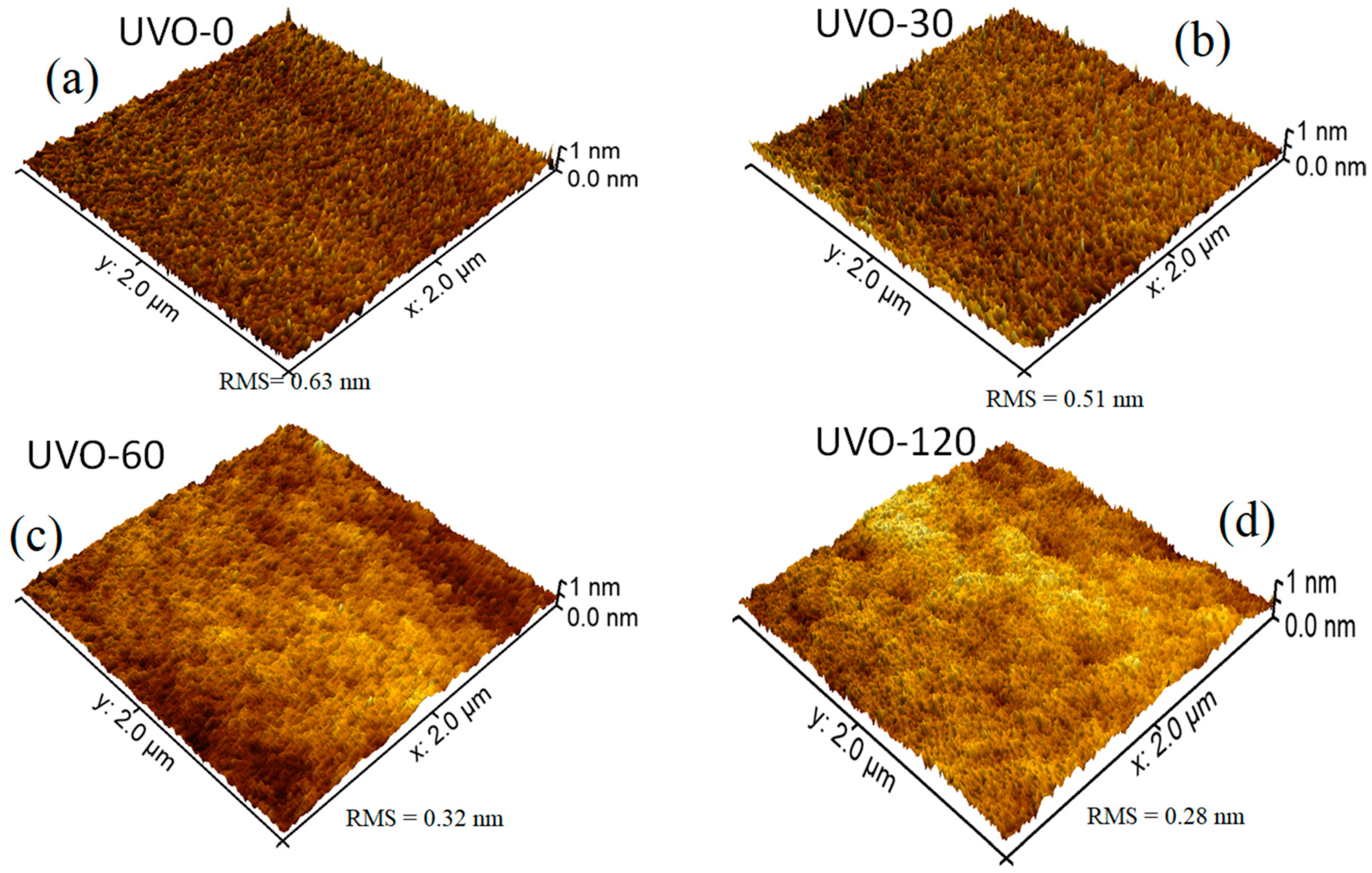
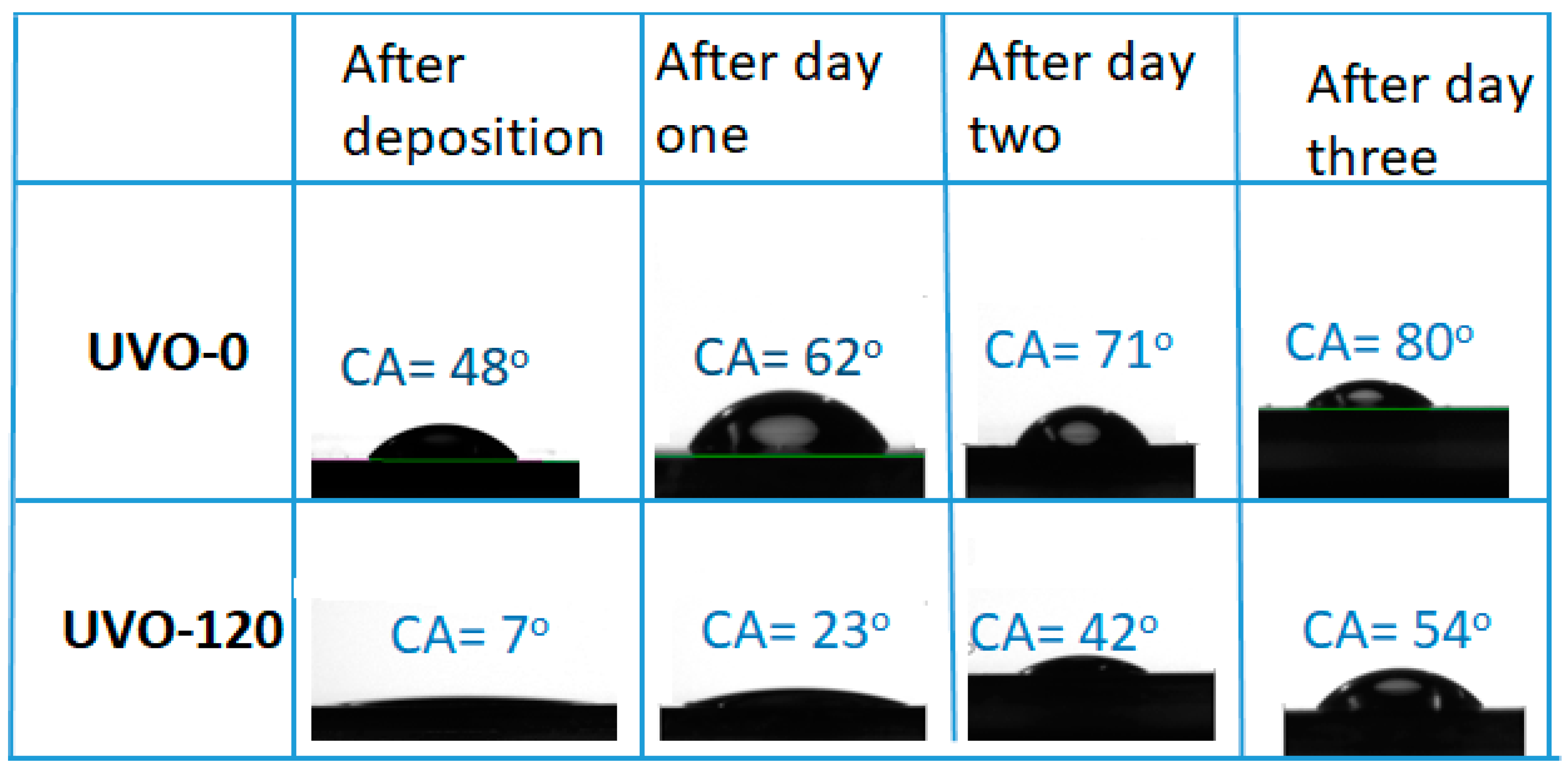
3.1. Surface Morphology and Wettability of the ZrOx Gate Dielectric Film

Figure 1 depicts the 3D AFM images (2 μm × 2 μm) for the ZrOx dielectric films at different UV-ozone exposure times (0–120 min), labelled as UVO-0, UVO-30, UVO-60, and UVO-120, respectively. Irrespective of the UVO treatment time, the ZrOx thin films demonstrated a plane surface morphology. The RMS roughnesses of the ZrOx thin film at different UVO exposure times of 0, 30, 60, and 120 min were evaluated to be 0.63 nm, 0.51 nm, 0.32 nm, and 0.28 nm, respectively, indicating that the ZrOx thin films are smooth and that increasing the UVO exposure time reduces the surface roughness of the films. This reduction relative to UVO treatment is due to the removal of organic residue by the oxygen radicals produced during the UVO process, leaving the surface of the film very smooth with a low RMS roughness [11]. A smooth surface is a convenient requirement for the dielectric layer in TFTs because the surface roughness of a dielectric layer strongly influences the quality of the interface with the channel layer, which in turn plays a significant role in the operation of the TFT device [10].
The wettability of the ZrOx dielectric surface was studied by measuring the water contact angle (CA), although the XRD pattern of the films indicated an amorphous structure (figure not shown). Figure 2 shows the droplet pictures alongside the mean CA values of water on both UVO-0 and UVO-120 treated ZrOx films. It also shows the changes in CA values with aging. In the observed results, the UVO-120-treated ZrOx dielectric is super-hydrophilic with a CA of 7°, while the UVO-0 film is hydrophilic with a CA of 48°.The intermediate treatment time (30 and 60 min) shows a CA value of 40°, which was 17° for UVO-30 and UVO-60, respectively. It is undoubtedly true that the UVO irradiation induces the presence of more OH-groups on the surface of the ZrOx film due to the simultaneous conversion between the Zr–O–Zr and Zr–OH groups, thereby increasing the hydrophilicity of the ZrOx film. A similar observation that supports this hypothesis was reported for ZrOx thin films grown by dip-coating [33]; however, for ZrOx dielectric films deposited by both sputtering [34] and electrochemical methods [35], a hydrophobic property was indicated. Gromyko et al. have also reported a difference in CA values for ZnO rods grown by both spray pyrolysis and electrodeposition methods [36].
Furthermore, after both samples were kept in a Petri-dish and allowed to age for three days, it was observed that the CA increased slightly in both UVO-120 and UVO-0 ZrOx dielectric films. This indicates that the surface properties of the ZrOx dielectric thin film can change owing to surface contamination from native carbon-containing species and that ZrOx test samples should be kept in special conditions. This is because, during the treatment process, the oxygen radicals are produced to remove the organic residues present on the film’s surface, leaving the ZrOx very active, and since test samples were not kept in any special conditions, this makes them vulnerable to native or environmental contaminants.

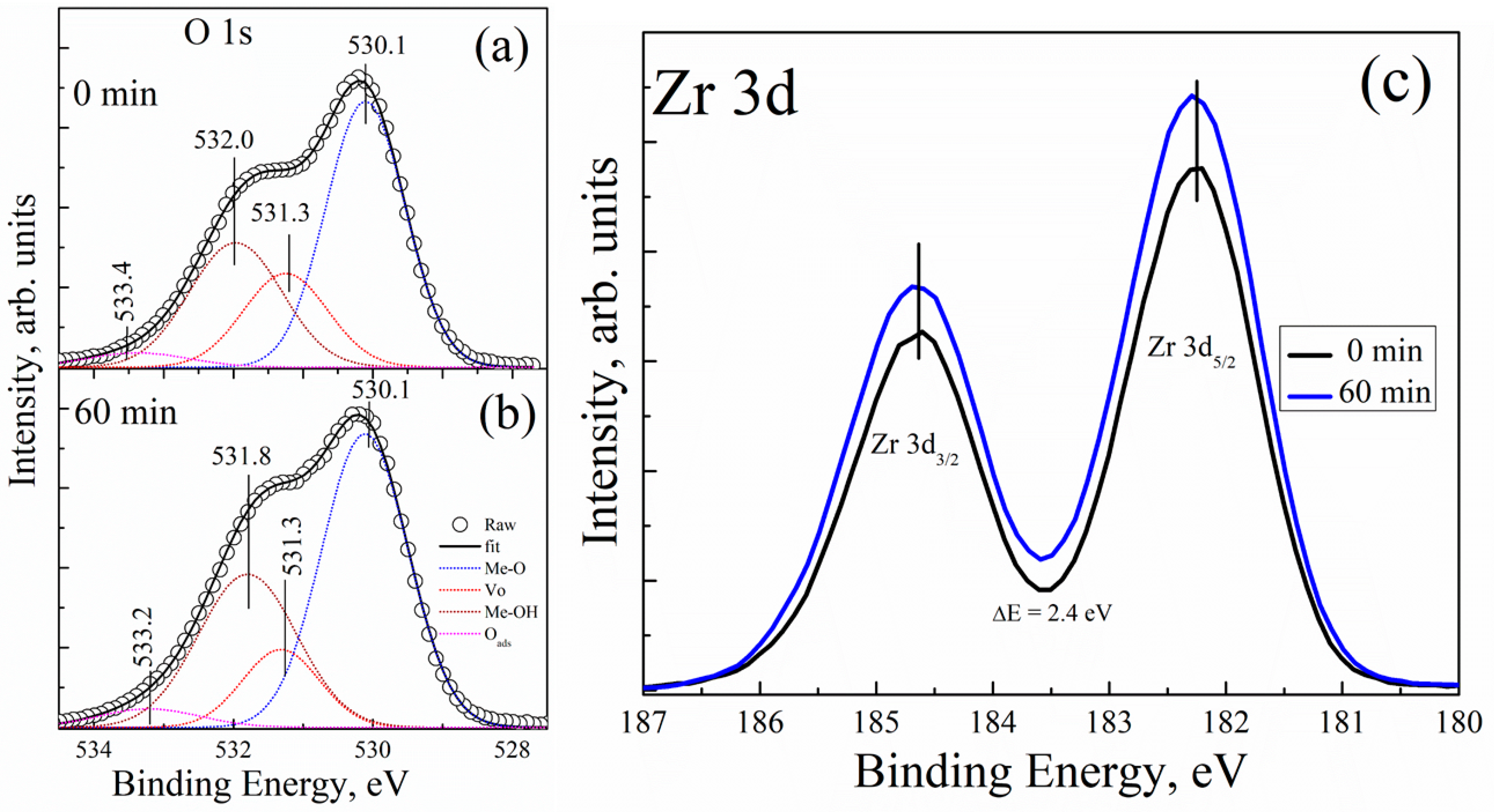
3.2. XPS Characterization of ZrOx Gate Dielectric Film

To study the surface composition of the deposited ZrOx thin films, XPS measurement was carried out. Figure 3 shows the survey XPS spectra for both the UVO (30–120)-treated and untreated ZrOx dielectric films. The spectra showed zirconium features at Zr 3s (432.4 eV), Zr 3d (182.0, 184.4 eV), Zr 3p (346, 322 eV), and Zr 4p (30.8 eV) [37,38]. The C 1s peak of adventitious carbon is present at 284.6 eV for all films including the UVO-treated samples. Auger peaks for O (KLL) are also detected at the high-binding-energy region. The peak intensity of Zr 3d increases slightly with increasing UVO exposure time. In addition, the intensity of the O 1s peak was increased. Here, our discussion will be based on the O 1s and Zr 3d core levels, making a correlation between the UVO-0 and UVO-60 samples.
Figure 4 shows the XPS spectra of the O 1s core level for two different UV-ozone treatment conditions. All the XPS spectra are asymmetric, and they were deconvoluted using Lorentzian–Gaussian (function pseudo-Voigt) distribution. Figure 4a displays the measured intensity of the O 1s core level of the UVO-0 sample; the peaks observed were fitted in four different components and centred at the binding energy (BE) values of 530.1, 531.3, 532.0, and 533.4 eV. The peak centred at 530.1 eV can be attributed to the BE of a well-bonded oxygen to zirconium (Me–O) in the ZrOx dielectric film lattice, while the peaks cantered at 531.3 imply the presence of an associated oxygen atom in the form of surface defects or vacancies in the film lattice (Vo). In addition, the peaks centred at 532.0 eV and 533.4 eV can be attributed to the oxygen in hydroxide-form (Me–OH) as a result of the high electronegativity of hydrogen atoms and the adsorbed oxygen (Oads), respectively [11,39]. Similarly, Figure 4b displays the measured intensity of the O 1s core level after a 60 minute UV-ozone treatment (UVO-60). The peaks on the XPS spectra are all located at BE and centred at BE values of 530.1, 531.3, 531.8, and 533.2 eV. The relatively weak peak component located at 533.2 eV is either due to oxygen connected with carbon or due to adsorbed oxygen in the form of moisture on the surface of the film [11,40,41]. This is certainly not connected to our samples, but to the environment (note that the films well sprayed directly on the Si-substrate were kept in a plastic box).
To resolve peak quantification properly, the peak ratios of all the components (MeO, Vo, −OH, H2Oads) found in the O 1s core level spectrum of UVO-0, UVO-30, UVO-60, and UVO-120 ZrOx dielectric films were calculated from integrated areas of the O 1s spectrum using Scofield’s cross-sections, and their corresponding values are summarized in Table 1. We observe that, by increasing the UVO treatment time from 0 min to 120 min, the ZrOx dielectric film demonstrated a slight increase in the [Me–OH]/[Me-O] component ratios, and a decrease in the [Vo]/[Me–O] ratio. It is confirmed that the UV–ozone treatment helps to eliminate the organic residues from the surface of the film, which makes our observation very reasonable, and a similar observation has been reported for solution-processed metal oxide films in [36,39,42]. The increase in the Me–OH component is an indication that the XPS study corresponds to the wettability study, suggesting that a high amount of –OH group at the film surface aided hydrophilicity in the UV-ozone treated ZrOx films.
Figure 4c shows the corresponding XPS spectra of the Zr 3d core level for both UVO-0 and UVO-60 ZrOx thin films. All the films showed the typical Zr 3d spectra with spin-orbit doublets (d5/2 = 182.3 eV, and d3/2 = 184.7 eV) separated by ~2.4 eV, which suggests the formation of ZrOx thin films [17,43]. A similar BE has been reported for Zr 3d in our previous study on Zr-doped TiO2 films by spray pyrolysis [17].
According to the material characterisation section, an oxygen radical is generated by the UVO treatment to remove organic impurities, thereby effecting a change in the chemical properties of the ZrOx film’s surface. This effect is evidently seen by the reduction in the donor defects (Vo) as well as an increase in the hydroxide group (Me-OH), actively changing the wettability and surface roughness of the ZrOx dielectric film. The UVO treatment serves as a good insight to reduce the thermal budget of solution-processing techniques—especially spray pyrolysis. Furthermore, the amorphous structure of the ZrOx dielectric film is essential to enhance the interface quality between different layers and to improve the electronic performance of the fabricated TFT device.

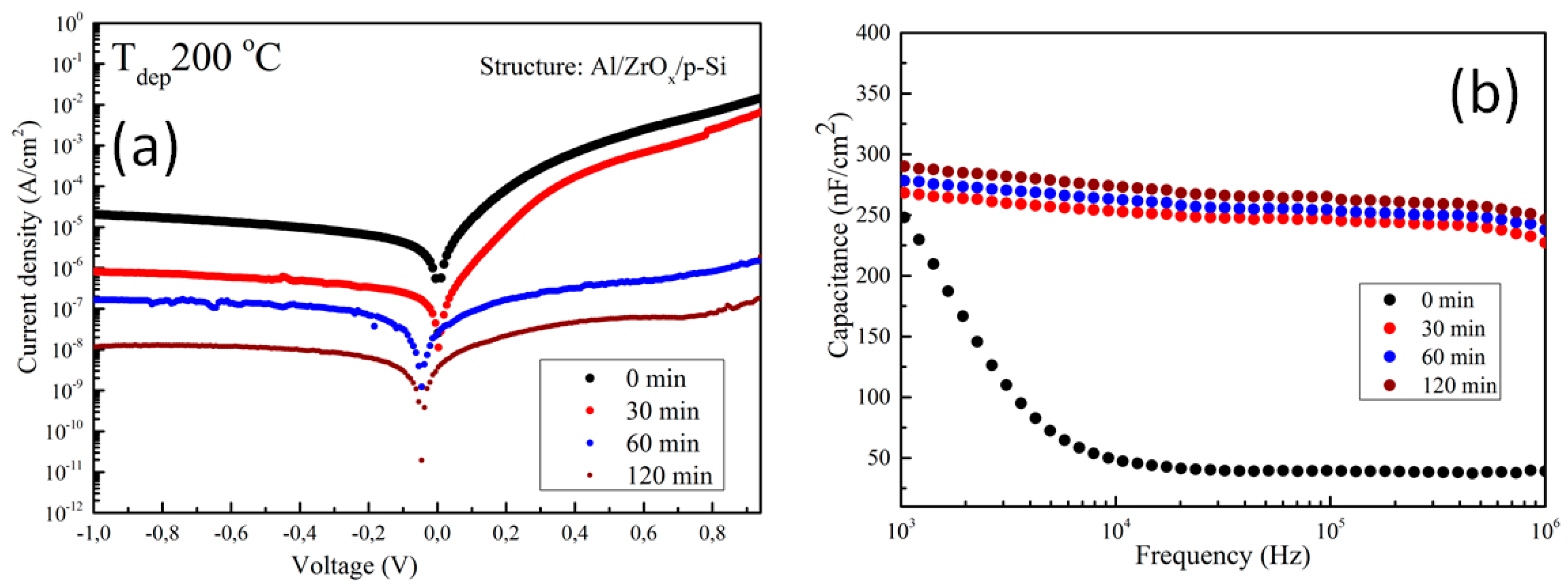
3.3. Electrical Characterization of ZrOx Capacitor

The electrical properties of the amorphous ZrOx dielectric film was assessed by fabricating a metal insulator semiconductor (MIS) capacitor with the structure Al/ZrO2/p-Si. Figure 5a shows the plot of leakage current density–voltage (J-V) for ZrOx dielectric films at different UVO treatment times. An asymmetric behavior can be seen due to the difference in the Schottky barrier height at the electrode interface. However, the leakage current density was calculated in the reverse bias regime, and it was found that the leakage current density in the UVO-0 ZrOx dielectric film is ~ 2.0 × 10⁻⁵ A/cm2 at 1 V. A similar behavior has been reported for a ZrOx dielectric deposited by atomic layer deposition (ALD) [44]. In contrast to the untreated sample, the UVO-treated samples demonstrated a remarkable reduction in leakage current density. Thus, by increasing the UVO treatment time to 30 min, the leakage current density was ~ 8.0 × 10⁻⁷ A/cm2, and a further increase in exposure time to 2 h yielded a leakage current density of ~ 1.0 × 10⁻⁸ A/cm2 at 1 V. It was reported that UV irradiation (λ > 185 nm) can produce hydroxyl radical (OH.) at a high quantum yield, which however aids the condensation reaction process of sol-gel metal oxide precursor films [25]. Therefore, it can be inferred that the reduction in the leakage current could be due to densification in the ZrOx thin film, which occurred as a result of the longer UVO exposure time, increases the formation of metal–oxygen lattices and lowers the amount of oxygen defects on the surface of the ZrOx thin film. A detailed explanation is given in the XPS study in Section 3.2. The zero-bias barrier heights of both the untreated and UVO-treated ZrOx dielectric were calculated by fitting the right part of Figure 6 into the following expression [42]:
B = k T q ln ( A A * T 2 I 0 )
where A is the effective area of the capacitor; A* is the effective Richardson constant, which is equal to 36 Acm−2T−2 for ZrO2, assuming an electron effective mass 0.3 mo for ZrOx; mo is the free electron mass [30,44]; k is the Boltzmann constant; and B is the Schottky barrier height.
The values of B extracted from Equation (1) amounted to 0.76, 0.84, 1.04, and 1.09 eV for UVO-0, UVO-30, UVO-60, UVO-120 samples, respectively. The increase in B could be due to surface changes at the ZrOx/electrode interface, which is caused by a change in surface energy due to UVO oxidative treatment. These values compared well with a similar report on a uniform and amorphous-ZrOx dielectric film deposited on the native tungsten oxide surface by ALD [44,45]. The observed changes in the barrier height showed that the energy barrier at the electrode/dielectric interfaces is influenced by chemical changes at the surface of dielectric apart from the effect of the image charge build-up at the electrode. To fully understand the changes in the observed barrier height, the effect of charge traps in the dielectric located at the electrode interface of the capacitor constituent layers must be considered [46]. The obtained result is a good indicator of the potential applicability of UVO treatment in reducing the process temperature of solution-processed dielectric films by changes in the surface chemistry of the ZrOx dielectric layer.
To account for the dielectric properties of the deposited ZrOx films, the capacitance–frequency (C–F) relation was measured at 0 V biased voltage. Figure 5b shows the C–F dispersion curve of ZrOx capacitors measured at different UVO treatment times. The untreated ZrOx dielectric demonstrated a high capacitance at the low frequency region, which suggests the contribution of ionic polarization [10]. On other hand, the UVO-treated samples exhibited a slight increase in capacitance (268, 272, and 290 nF/cm2 for UVO-30, UVO-60, and UVO-120 samples, respectively), which was stable in the high-frequency region. The result obtained from the UVO-treated samples revealed that, by increasing the UVO exposure time, the contributions from the interface or native oxide capacitance can be eliminated. This result concurs with the AFM and XPS results on the condensation and defect reduction from the surface of the UVO treated ZrOx dielectric films.
According to the equation   C = ε 0 κ A / d , where C is capacitance, ε 0   is the permittivity of free space, κ is the relative permittivity, A is the contact area, and d is the ZrOx film thickness (~ 20 nm), the relative permittivity (κ) of all the deposited ZrOx films was calculated. As with the capacitance, the value of κ increases slightly from 5.8 to 6.6 with an increase in the UVO exposure time. It can be inferred from our previous study on ZrOx dielectric films by spray pyrolysis that thermal annealing (~800 °C) was needed to obtain a κ value of 4.8 [19]. However, in this study, with UVO treatment, a κ value of 6.6 is obtained, thus indicating the advantage of UVO treatment in improving the properties of high-κ oxide dielectric films.
Generally, we observed that the value of κ is smaller compared to the most anticipated theoretical κ value for ZrOx. This could be due to the influence of interfacial barriers in the film’s microstructure during deposition. Also, the sprayed deposited ZrOx films are amorphous and inevitably contain pores because of the low deposition temperature. Nevertheless, this does not limit the performance of our film, as a similar value has been reported for a ZrOx dielectric deposited by spin-coating in [2,11].

3.4. TFT Characterization of the Fabricated IGZO-Based Device

In order to ascertain the applicability of the deposited sprayed ZrOx film in TFT, we fabricated a TFT with a bottom-gate–top-contact configuration, and the alignment between the channel and dielectric layer was patterned and staggered to reduce the probability of the source/drain infringing on the channel. Both the architecture and electrical performance of the TFT devices are shown in Figure 6, with the extracted electrical parameters presented in Table 2. All transistors which were fabricated are working and show a clear gate dependence corresponding to the n-type channel. The transfer characteristics of the IGZO based devices, which were measured in forward and backward sweeps for both the untreated and the UVO-treated ZrOx gate dielectric, are shown in Figure 6b,d respectively. The device with the untreated gate dielectric showed a poor performance with a negative Von of about −2 V, which means that the device was working in a depletion mode, and the ratio between the on current and off current (Ion/Ioff) was very low at about 40 the leakage current (IGS) flowing through the gate was about 3.4 × 10⁻² A. However, the device with a UVO-treated ZrOx gate as its dielectric layer showed better electrical performance with negligible hysteresis, which later improved by increasing the UVO exposure time. The Von changed from −0.3 V to 0.02 V when the UVO treatment time was increased from 30 to 120 min, respectively, indicating that the device changes its mode of operation from the depletion mode to enhancement mode. The positive shift in the device Von could stem from the influence of the UV treatment influencing the surface potential of the ZrOx dielectric. As the UV–ozone exposure time increases, a new chemical state is induced on the surface of the ZrOx dielectric which is capable of effecting high electron trapping at the interface, particularly when a gate bias is applied to the device. Therefore, in order to compensate the charge, more mobile hole charges are induced, which explains the positively shifted threshold voltage of the TFT [47].
This result concurs with the wettability measurement as well as the Schottky barrier determination, demonstrating an increase in the energy barrier height caused by changes in the surface potential of the ZrOx dielectric layer during the UV-ozone treatment. Furthermore, the magnitudes of the on–off current ratio, Ion/Ioff, are 1 × 10³, 0.4 × 10⁴, and 1 × 10⁴ when the UVO treatment time increases from 30, 60 to 120 min, respectively. The Figure 6c shows the typical output characteristic curve for the 60 min UVO-treated ZrOx gate dielectric TFT. It can be seen that the UVO-treated TFTs exhibit typical n-type channel conduction behavior with a clear pinch-off voltage and current saturation.
The fabricated TFT parameters, such as saturation mobility (µsat), threshold voltage and sub-threshold slope, were extracted from the following equation [45] and are summarized in Table 2.
I d =   ( C Z r O B μ s a t 2 L ) ( V G   V T ) 2
where C Z r O is the gate dielectric capacitance per unit area, B and L are the channel width and length, V G is the gate voltage, and V T is the threshold voltage, which was determined in the saturation regim by the fitting of the curve of I d 1 2 versus V G and extrapolating the linear part to the V G axis. As expected, the devices with a UVO-treated ZrOx dielectric layer have better mobility, which increases from 2.9 to 8.4 cm2 V−1S−1 with increasing treatment time (from 30 to 120 min).
The observed changes in mobility may be due to an increase in the capacitance of the ZrOx gate dielectric layer when exposed to UVO treatment. According to Dong et al. [24] in their recent publication, there is the possibility of using UVO treatment to improve the device performance of InO/ZrOx TFTs. Also, Carlos et al. [46] demonstrated the possibility of reducing the gate leakage current of IGZO/AlOx TFT devices by using a very powerful UV lamp. The device demonstrated a positive shift in its threshold voltage (Vth) from −0.12 to 0.01 V, and a slight decrease in the sub-threshold slope (S) with increasing UVO treatment. The positive Vth indicated that the device can completely be switched off and can be turned on by a voltage as minimal as 0.01 V. In addition, the small S value extracted from the TFTs may be attributed to the large area capacitance at the ZrOx gate dielectric layer and smoother surface due to the UVO cleaning of the layer, thereby improving the interface quality between IGZO and ZrOx [11,39].

4. Conclusions

In summary, we have demonstrated the possibility of lowering the processing temperature of ultrasonically sprayed amorphous ZrOx thin films by introducing UV–ozone post deposition treatment. It was confirmed by XPS and wettability measurement that by increasing the UVO exposure time, the surface of the sprayed ZrOx films became less defective and hydrophilic, with a contact angle of 7°, indicating the removal of organic impurities associated with the precursor reagents from the surface of the film. The AFM result showed that the deposited ZrOx film was smooth, and the surface roughness was reduced from 0.63 nm (UVO-0 film) to 0.28 nm (UVO-120 film). Finally, to demonstrate the electrical performance of the film, a MOS-capacitor was fabricated, and we observed a reduction in the leakage current density by three orders of magnitude by increasing the UV–ozone treatment time. The UVO treated ZrOx capacitor attained desirable dielectric properties, such as a low leakage current density of 10−8 A/cm2, a capacitance of 290 nF/cm2 and relative permittivity of 6.6 (both at 1 kHz).
As a proof of concept, both untreated and UV–ozone post deposition-treated ZrOx thin film were used as the gate dielectric in TFT. The fabricated TFT with the treated ZrOx films demonstrated an improved performance compared to a device produced with the untreated ZrOx dielectric thin film. The former operates in an enhancement mode (Von > 0), with low power consumption and a high saturation mobility of 8 cm2 V-1s-1. UV-ozone treatment is the key to developing a metal oxide film at low temperature by wet chemical techniques. This concept thus opens the potential application of ultrasonic spray technology in flexible electronics.

Author Contributions

Conceptualization, A.T.O. and I.O.A.; methodology, A.T.O., D.G., and A.K.; software, A.T.O., A.K., and A.M.; validation, M.K., I.O.A. and A.T.O.; formal analysis, A.T.O.; investigation, A.T.O.; resources, D.G., L.P.; data curation, A.T.O., I.O.A.; writing—original draft preparation, A.T.O.; writing—review and editing, A.T.O., I.O.A., L.P., M.K.; visualization, A.T.O.; supervision, I.O.A., L.P., M.K.; project administration, I.O.A.; funding acquisition, I.O.A., M.K., L.P. All authors have read and agreed to the published version of the manuscript.

Funding

This study was financially supported by the Estonian Ministry of Education and Research project IUT194, and by the European Union through the European Regional Development Fund project TK141 “Advanced materials and high-technology devices for energy recuperation systems” and by FCT—Portuguese Foundation for Science and Technology, Reference UID/CTM/50025/2019 and FCT/MCTES. The authors acknowledge the European Commission under project NewFun (ERC-StG-2014, GA 640598). This work was also supported by the FEDER funds through the COMPETE 2020 Program and the National Funds through the FCT − Portuguese Foundation for Science and Technology under Project POCI-01-0145-FEDER-007688, Reference UID/CTM/50025, project PapEl, reference PTDC/CTM-NAN/5172/2014 and project CHIHC, reference PTDC/NAN-MAT/32558/2017.

Acknowledgments

Abayomi T. Oluwabi would also like to thank the Archimedes foundation for financing research mobility, through the “DoRa Plus Action 1”. D. Gaspar acknowledges the support from FCT - Portuguese Foundation for Science and Technology through the AdvaMTech PhD program scholarship PD/BD/52627/2014. Dr. Rainer Traksmaa is thanked for the AFM measurement, and Dr. Erki Kärber for the XPS measurement.

Conflicts of Interest

The authors declare no conflict of interest.

References

  1. Petti, L.; Münzenrieder, N.; Vogt, C.; Faber, H.; Büthe, L.; Cantarella, G.; Bottacchi, F.; Anthopoulos, T.D.; Tröster, G. Metal Oxide Semiconductor Thin-film Transistors for Flexible Electronics. Appl. Phys. Rev. 2016, 3, 021303. [Google Scholar] [CrossRef] [Green Version]
  2. Liu, G.X.; Liu, A.; Shan, F.K.; Meng, Y.; Shin, B.C.; Fortunato, E.; Martins, R. High-performance fully amorphous bilayer metal-oxide thin film transistors using ultra-thin solution-processed ZrOx dielectric. Appl. Phys. Lett. 2014, 105, 113509. [Google Scholar] [CrossRef]
  3. Avasthi, S.; Nagamatsu, K.A.; Jhaveri, J.; McClain, W.E.; Man, G.; Kahn, A.; Schwartz, J.; Wagner, S.; Sturm, J.C. Double-heterojunction Crystalline Silicon Solar Cell Fabricated at 250 °C with 12.9% Efficiency. In Proceedings of the 2014 40th IEEE Photovoltaic Specialist Conference, Denver, CO, USA, 8–13 June 2014; p. 949. [Google Scholar]
  4. Korotcenkov, G. Metal Oxides for Solid-state Gas Sensors: What Determines Our Choice? Mater. Sci. Eng. B 2007, 139, 1–23. [Google Scholar] [CrossRef]
  5. Ielmini, D. Resistive Switching Memories Based on Metal Oxides: Mechanisms, Reliability and Scaling. Semicond. Sci. Technol. 2016, 31, 063002. [Google Scholar] [CrossRef]
  6. Kim, K.M.; Jeong, D.S.; Hwang, C.S. Nanofilamentary Resistive Switching in Binary Oxide System; a Review on the Present Status and Outlook. Nanotechnology 2011, 22, 254002. [Google Scholar] [CrossRef]
  7. Chang, C.Y.; Huang, W.K.; Wu, J.L.; Chang, Y.C.; Lee, K.T.; Chen, C.T. Room-temperature solution-processed n-doped zirconium oxide cathode buffer layer for efficient and stable organic and hybrid perovskite solar cells. Chem. Mater. 2015, 28, 242–251. [Google Scholar] [CrossRef]
  8. Yoon, H.J.; Bang, K.S.; Lim, J.W.; Lee, S.Y. Optical properties of zirconium oxide thin films for semi-transparent solar cell applications. J. Mater. Sci. Mater. Electron. 2016, 27, 11358–11365. [Google Scholar] [CrossRef]
  9. Xiao, D.; He, G.; Sun, Z.; Lv, J.; Jin, P.; Zheng, C.; Liu, M. Microstructure, optical and electrical properties of solution-derived peroxo-zirconium oxide gate dielectrics for CMOS application. Ceram. Int. 2016, 42, 759–766. [Google Scholar] [CrossRef]
  10. Branquinho, R.; Salgueiro, D.; Santos, L.; Barquinha, P.; Pereira, L.; Martins, R.; Fortunato, E. Aqueous Combustion Synthesis of Aluminum Oxide Thin Films and Application as Gate Dielectric in GZTO Solution-Based TFTs. ACS Appl. Mater. Interfaces 2014, 6, 19592–19599. [Google Scholar] [CrossRef]
  11. Zhu, C.; Liu, A.; Liu, G.; Jiang, G.; Meng, Y.; Fortunato, E.; Martins, R.; Shan, F. Low-temperature, nontoxic water-induced high-k zirconium oxide dielectrics for low-voltage, high-performance oxide thin-film transistors. J. Mater. Chem. C 2016, 4, 10715–10721. [Google Scholar] [CrossRef]
  12. Park, J.H.; Yoo, Y.B.; Lee, K.H.; Jang, W.S.; Oh, J.Y.; Chae, S.S.; Baik, H.K. Low-Temperature, High-Performance Solution-Processed Thin-Film Transistors with Peroxo-Zirconium Oxide Dielectric. ACS Appl. Mater. Interfaces 2013, 5, 410–417. [Google Scholar] [CrossRef] [PubMed]
  13. Lee, C.G.; Dodabalapur, A. Solution-processed zinc–tin oxide thin-film transistors with low interfacial trap density and improved performance. Appl. Phys. Lett. 2010, 96, 243501. [Google Scholar] [CrossRef]
  14. Ha, T.J.; Dodabalapur, A. Photo stability of solution-processed low-voltage high mobility zinc-tin-oxide/ZrO2 thin-film transistors for transparent display applications. Appl. Phys. Lett. 2013, 102, 123506. [Google Scholar] [CrossRef]
  15. Zhao, X.; Wang, S.; Li, A.; Ouyang, J.; Xia, G.; Zhou, J. Universal solution-processed high-k amorphous oxide dielectrics for high-performance organic thin film transistors. RSC Adv. 2014, 4, 14890–14895. [Google Scholar] [CrossRef]
  16. Oja Acik, I.; Mere, A.; Krunks, M.; Nisumaa, R.; Solterbeck, C.-H.; Es-Souni, M. Structural and electrical characterization of TiO2 films grown by spray pyrolysis. Thin Solid Film. 2006, 515, 674–677. [Google Scholar]
  17. Juma, A.; OjaAcik, I.; Oluwabi, A.T.; Mere, A.; Mikli, V.; Danilson, M.; Krunks, M. Zirconium doped TiO2 thin films deposited by chemical spray pyrolysis. App. Surf. Sci. 2016, 387, 539–545. [Google Scholar] [CrossRef]
  18. Oluwabi, A.T.; Juma, A.O.; Oja Acik, I.; Mere, A.; Krunks, M. Effect of Zr doping on the structural and electrical properties of spray deposited TiO2 thin film. Proc. Est. Acad. Sci. 2018, 67, 147–157. [Google Scholar] [CrossRef]
  19. Oluwabi, A.T.; Oja Acik, I.; Katerski, A.; Mere, A.; Krunks, M. Structural and electrical characterisation of high-k ZrO2 thin films deposited by chemical spray pyrolysis method. Thin Solid Film. 2018, 662, 129–136. [Google Scholar] [CrossRef]
  20. Morvillo, P.; Diana, R.; Mucci, A.; Bobeica, E.; Ricciardi, R.; Minarina, C. Influence of annealing treatments on solution-processed ZnO film deposited on ITO substrate as electron transport layer for inverted polymer solar cells. Sol. Energy Mater. Sol. Cells 2015, 141, 210–217. [Google Scholar] [CrossRef]
  21. Banger, K.; Yamashita, Y.; Mori, K.; Peterson, R.; Leedham, T.; Rickard, J.; Sirringhaus, H. Low-temperature, high-performance solution-processed metal oxide thin-film transistors formed by a ‘sol–gel on chip’ process. Nat. Mater. 2011, 10, 45–50. [Google Scholar] [CrossRef]
  22. Rim, Y.S.; Chen, H.; Song, T.B.; Bae, S.H.; Yang, Y. Hexaaqua metal complexes for low-temperature formation of fully metal oxide thin-film transistors. Chem. Mater. 2015, 27, 5808–5812. [Google Scholar] [CrossRef]
  23. Jeong, W.H.; Kim, D.L.; Kim, H.J. Accelerated formation of metal oxide thin film at 200 C using oxygen supplied by a nitric acid additive and residual organic suction vacuum annealing for thin-film transistor applications. ACS Appl. Mater. Interfaces 2013, 5, 9051–9056. [Google Scholar] [CrossRef] [PubMed]
  24. Donga, X.; Xia, G.; Zhang, Q.; Li, L.; Gong, H.; Bi, J.; Wang, S. Room-temperature UV-ozone assisted solution process for zirconium oxide films with high dielectric properties. Ceram. Int. 2017, 43, 15205–15213. [Google Scholar] [CrossRef]
  25. Leppäniemi, J.; Ojanperä, K.; Kololuoma, T.; Huttunen, O.-H.; Dahl, J.; Tuominen, M.; Laukkanen, P.; Majumdar, H.; Alastalo, A. Rapid low-temperature processing of metal-oxide thin film transistors with combined far ultraviolet and thermal annealing. Appl. Phys. Lett. 2014, 105, 113514. [Google Scholar] [CrossRef]
  26. Wang, B.; Yu, X.; Guo, P.; Huang, W.; Zeng, L.; Zhou, N.; Chi, L.; Bedzyk, M.J.; Chang, R.P.; Marks, T.J. Solution-processed all-oxide transparent high-performance transistors fabricated by spray-combustion synthesis. Adv. Electron. Mater. 2016, 2, 1500427. [Google Scholar] [CrossRef]
  27. Kim, M.G.; Kanatzidis, M.G.; Facchetti, A.; Marks, T.J. Low-temperature fabrication of high-performance metal oxide thin-film electronics via combustion processing. Nat. Mater. 2011, 10, 382–388. [Google Scholar] [CrossRef]
  28. Park, J.H.; Oh, J.Y.; Han, S.W.; Lee, T.I.; Baik, H.K. Low-temperature, solution-processed ZrO2: B thin film: A bifunctional inorganic/organic interfacial glue for flexible thin-film transistors. ACS Appl. Mater. Interfaces 2015, 7, 4494–4503. [Google Scholar] [CrossRef]
  29. Kim, Y.H.; Heo, J.S.; Kim, T.H.; Park, S.; Yoon, M.H.; Kim, J.; Oh, M.S.; Yi, G.R.; Noh, Y.Y.; Park, S.K. Flexible metal-oxide devices made by room-temperature photochemical activation of sol-gel films. Nature 2012, 489, 128–132. [Google Scholar] [CrossRef]
  30. Reyna-Garcia, G.; Garcia-Hipolota, M.; Guzman-Mandoza, J.; Aguilar-Frutis, M.; Falcony, C. Electrical, optical and structural characterization of high-k dielectric ZrO2 thin films deposited by the pyrosol technique. J. Mater. Sci. Mater. Electron. 2004, 15, 439–446. [Google Scholar] [CrossRef]
  31. Santos, E.R.; Burini, E.C.; Wang, S.H. UV-ozone generation from modified high intensity discharge mercury vapor lamps for treatment of indium tin oxide films. Ozone Sci. Eng. 2012, 34, 129–135. [Google Scholar] [CrossRef] [Green Version]
  32. Gaspar, D.; Martins, J.; Bahubalindruni, P.; Pereira, L.; Fortunato, E.; Martins, R. Planar Dual-Gate Paper/Oxide Field Effect Transistors as Universal Logic Gates. Adv. Electron. Mater. 2018, 4, 1800423. [Google Scholar] [CrossRef]
  33. Rudakova, A.V.; Maevskaya, M.V.; Emeline, A.V.; Bahnemann, D.W. Light-Controlled ZrO2 Surface Light-Controlled ZrO2 Surface Hydrophilicity. Sci. Rep. 2016, 6, 34285. [Google Scholar] [CrossRef] [PubMed] [Green Version]
  34. Patela, U.S.; Patel, K.H.; Chauhan, K.V.; Chawla, A.K.; Rawal, S.K. Investigation of various properties for zirconium oxide films synthesised by sputtering. Proc. Technol. 2016, 23, 336–343. [Google Scholar] [CrossRef] [Green Version]
  35. Hao, Y.; Soolaman, D.M.; Yu, H.-Z. Controlled Wetting on Electrodeposited Oxide Thin Films: From Hydrophilic to Superhydrophobic. J. Phys. Chem. C 2013, 117, 7736–7743. [Google Scholar] [CrossRef]
  36. Gromyko, I.; Krunks, M.; Dedova, T.; Katerski, A.; Klauson, D.; Oja Acik, I. Surface properties of sprayed and electrodeposited ZnO rod layers. Appl. Surf. Sci. 2017, 405, 521–528. [Google Scholar] [CrossRef]
  37. Cabillo, G.; Lillo, L.; Caro, C.; Buono-Core, G.E.; Chornik, B.; Soto, M.A. Structure and optical characterization of photochemically prepared ZrO2 thin films doped with erbium and europium. J. Non-Cryst. Solids 2008, 354, 3919–3928. [Google Scholar] [CrossRef]
  38. Zhang, N.L.; Song, Z.T.; Wan, Q.; Shen, Q.W.; Lin, C.L. Interfacial and microstructural properties of zirconium oxide thin films prepared directly on silicon. Appl. Surf. Sci. 2002, 202, 126–130. [Google Scholar] [CrossRef]
  39. Umeda, K.; Miyasako, T.; Sugiyama, A.; Tanaka, A.; Suzuki, M.; Tokumitsu, E.; Shimoda, T. Impact of UV/O3 treatment on solution-processed amorphous InGaZnO4 thin-film. J. Appl. Phys. 2013, 113, 184509. [Google Scholar] [CrossRef]
  40. Chun, M.; Moon, M.-J.; Park, J.; Kang, Y.-C. Physical and Chemical Investigation of Substrate Temperature Dependence of Zirconium Oxide Films on Si (100). Bull. Korean Chem. Soc. 2009, 30, 2729–2734. [Google Scholar]
  41. Jiazhen, S.; TaeHyun, H.; Hyun-Mo, L.; KyoungRok, K.; Masato, S.; Junghwan, K.; Hideo, H.; Jin-Seong, P. Amorphous IGZO TFT with High Mobility of ~70 cm2/(Vs) via Vertical Dimension Control Using PEALD. ACS Appl. Mater. Interfaces 2019, 11, 40300–40309. [Google Scholar]
  42. Islam, R.; Chen, G.; Ramesh, P.; Suh, J.; Fuchigami, N.; Lee, D.; Littau, K.A.; Weiner, K.; Collins, R.T.; Saraswat, K.C. Investigation of the changes in electronic properties of Nickel oxide due to UV/ozone treatment. Appl. Mater. Interfaces 2017, 9, 17201–17207. [Google Scholar] [CrossRef]
  43. Kumar, A.; Mondal, S.; Koteswara, K.S.R. Low temperature solution processed high-ZrO2 gate dielectrics fornanoelectonics. Appl. Surf. Sci. 2016, 370, 373–379. [Google Scholar] [CrossRef]
  44. Lee, S.-Y.; Kim, H.; Mclntyre, P.C.; Saraswat, K.C.; Byun, J.-S. Atomic layer deposition of ZrO2 on W for metal-insulator-metal capacitor application. Appl. Phys. Lett. 2003, 82, 2874. [Google Scholar] [CrossRef]
  45. Fu-Chien, C. A Review on Conduction Mechanisms in Dielectric Films. Adv. Mater. Sci. Eng. 2014, 2014, 578168. [Google Scholar]
  46. Carlos, E.; Branquinho, R.; Kiazadeh, A.; Barquinha, P.; Martins, R.; Fortunato, E. UV-mediated photochemical treatment for low-temperature oxide based thin film transistor. Appl. Mater. Interfaces 2016, 45, 31100–31108. [Google Scholar] [CrossRef] [PubMed]
  47. Huang, W.; Fan, H.; Zhuang, X.; Yu, J. Effect of uv/ozone treatment on polystyrene dielectric and its application on organic field-effect transistors. Nanoscale Res. Lett. 2014, 9, 479. [Google Scholar] [CrossRef] [Green Version]
Figure 1. Atomic force microscopy (AFM) morphologies of (a) UV–ozone (UVO)-0 (untreated), (b) UVO-30, (c) UVO-60, and (d) UVO-120 treated ZrOx dielectric thin films.
Materials 13 00006 g001
Figure 2. Images of the water contact angle (CA) measurements for both treated (UVO-120) and untreated (UVO-O) ZrOx thin film and their corresponding contact angles after aging for three days.
Materials 13 00006 g002
Figure 3. X-ray photoelectron spectroscopy (XPS) survey spectra of ZrOx thin films at different UV–ozone treatment times.
Materials 13 00006 g003
Figure 4. XPS spectra of the O 1s core level for (a) 0 minute and (b) 60 minutes of UVO treatment of the ZrOx dielectric film; the corresponding XPS spectra for the Zr 3d core level for the ZrOx dielectric film is presented in (c).
Materials 13 00006 g004
Figure 5. Electrical characterization of the metal insulator semiconductor (MIS) device made from ZrOx dielectric: (a) current–voltage curve under positive and negative biases; and (b) capacitance–frequency dispersion curve in the range between 1 kHz and 1 MHz at different UV–ozone treatment times. The device has an Al/ZrOx/p–Si structure.
Materials 13 00006 g005
Figure 6. Thin film transistor (TFT) characteristics of indium gallium zinc oxide (IGZO)/ZrOx devices. (a) Schematic representation of device structure, (b) transfer and output (inset) characteristics of the devices with an untreated ZrOx gate dielectric, (c) output characteristic of a TFT-device with a treated ZrOx gate dielectric for 60 min, and (d) the transfer performance of the TFT devices with a treated ZrOx gate dielectric at different UV–ozone exposure times.
Materials 13 00006 g006
Table 1. Binding energy of O 1s components and their corresponding ratios for UVO-0, UVO-30, UVO-60 and UVO-120 ZrOx dielectric films.
Treatment
Conditions
Binding Energy (eV)Component Ratios
Me-OVoMe-OHOH ads[Vo]/[Me-O][Me-OH]/[Me-O]
UVO-0530.1531.3532.0533.40.650.94
UVO-30530.1531.3532.0533.30.591.04
UVO-60530.1531.3531.8533.20.411.10
UVO-120530.1531.4532.8533.20.381.22
Table 2. Summary of the extracted TFT parameters for an average of ten IGZO/ZrOx devices at different UV–ozone treatment times.
Treatment
Conditions
Von
(V)
Ion/IoffVth
(V)
S
(V.dec−1)
µsat.
cm2 V1S1
IGS at VGS = 5 V
(A)
As-dep−2.0 ± 1.0~40~0.02~3.4 × 10⁻²
30 min−0.3 ± 0.02~1.0 × 10³−0.12 ± 0.020.27 ± 0.022.9 ± 0.5~7.4 × 10⁻⁵
60 min−0.12 ± 0.1~0.4 × 1040.02 ± 0.010.22 ± 0.017.0 ± 0.01~2.3 × 10⁻⁵
120 min0.02 ± 0.01~1.0 ×1040.01 ± 0.0050.21 ± 0.018.4 ± 0.01~3.8 × 10⁻⁷

