Article

First-Principles Investigation of the Adsorption Behaviors of CH2O on BN, AlN, GaN, InN, BP, and P Monolayers

1
School of Mechanical and Electronic Engineering, Guilin University of Electronic Technology, Guilin 541004, China
2
EEMCS Faculty, Delft University of Technology, 2628 Delft, The Netherlands
*
Author to whom correspondence should be addressed.
Materials 2019, 12(4), 676; https://doi.org/10.3390/ma12040676
Submission received: 29 January 2019 / Revised: 15 February 2019 / Accepted: 18 February 2019 / Published: 25 February 2019
(This article belongs to the Special Issue Fabrication of 1D and 2D Nanomaterials)

Abstract

:
CH2O is a common toxic gas molecule that can cause asthma and dermatitis in humans. In this study the adsorption behaviors of the CH2O adsorbed on the boron nitride (BN), aluminum nitride (AlN), gallium nitride (GaN), indium nitride (InN), boron phosphide (BP), and phosphorus (P) monolayers were investigated using the first-principles method, and potential materials that could be used for detecting CH2O were identified. The gas adsorption energies, charge transfers and electronic properties of the gas adsorption systems have been calculated to study the gas adsorption behaviors of CH2O on these single-layer materials. The electronic characteristics of these materials, except for the BP monolayer, were observed to change after CH2O adsorption. For CH2O on the BN, GaN, BP, and P surfaces, the gas adsorption behaviors were considered to follow a physical trend, whereas CH2O was chemically adsorbed on the AlN and InN monolayers. Given their large gas adsorption energies and high charge transfers, the AlN, GaN, and InN monolayers are potential materials for CH2O detection using the charge transfer mechanism.

1. Introduction

In the past years monolayer 2D materials have elicited increasing attention because of their superior thermal, mechanical, and optoelectronic properties [1,2]. Therefore, studies that focus on the applications of monolayer materials are attractive because these materials exhibit excellent performance in both gas sensors and optoelectronic devices [2,3]. With the development of the research, an increasing number of monolayer materials, such as boron nitride (BN) [4] and antimonene [5], have been predicted and synthesized. Within the monolayer materials, the family of nitrides has become a popular research material in optoelectronic and electronic applications because of their outstanding properties [4,6]. Two-dimensional (2D) BN, aluminum nitride (AlN), gallium nitride (GaN), and indium nitride (InN) materials exhibit a graphene-like honeycomb structure with band gaps of 4.47 [4], 2.9 [6], 2.16 [7], and 1.48 eV [8], respectively. Rao et al. successfully prepared graphene-like analogs of BN flakes, which can be applied in the preparation of composites [9]. It has been reported that an AlN monolayer can epitaxially grow on Ag (111) via plasma-assisted molecular beam deposition [10]. Graphene-like GaN monolayers exhibit high electronic mobility, indicating their excellent potential for application in nanoelectronics [11]. Moreover, first-principles calculations demonstrate that hexagonal InN monolayers exhibit excellent electronic properties [8], and InN nanowires can be experimentally prepared [12]. Furthermore, the boron phosphide (BP) monolayer is theoretically predicted to exhibit remarkable electronic properties [13], and a layered BP was prepared by Li et al. [14]. In addition, the blue phosphorus (P) monolayer was synthesized by Zhang et al. [15], and the monolayer P exhibited a remarkable potential for applications in nanodevices [16]. Ga, In, and P are critical raw materials for the EU while they are not critical for China [17], and the application of 2D materials can significantly reduce the amount of material necessary for the realization of a sensor.
Owing to their atomic thicknesses, large surface areas, and excellent electrical properties, monolayer 2D materials can become the new-generation sensitive materials of gas sensors [18]. In a previous study, the electronic characteristics of the monolayer materials were altered using some special adsorbed gas molecules [3]. Based on the investigation conducted by Zhou et al., P was ultrasensitive to NO, NO2, and NH3 gas molecules, indicating that the P monolayer is a potential material for the detection of these molecules [19]. Furthermore, antimonene was sensitive to NO, NH3, and SO2 gas molecules. Its electronic characteristics are altered after these gas molecules are adsorbed [3]. The investigation conducted by Li et al. indicated that monolayer MoS2 was suitable for detecting the O2, NO, and NO2 molecules [20]. Therefore, the application of monolayer materials in gas sensors is currently considered to be a popular research field.
Furthermore, various theoretical works and experiments have proved that BN, AlN, GaN, InN, BP, and P are potential sensitive materials that can be applied in gas sensors [19,21,22,23,24,25]. For example, ultrathin BN nanosheets can be used for detecting ethanol at high operating temperatures, and Lin et al. reported that the gas sensors showed a rapid response and recovery [21]. According to the investigation conducted by Wang et al., the AlN monolayer was suitable for detecting H2, CO, CO2, NO, and O2 via the charge transfer mechanism [22]. CH2O is a common toxic gas molecule that may lead to asthma and dermatitis in humans. Thus, detecting its presence and removing it from the environment is considered to be important. To the best of our knowledge, various traditional materials, such as ZnO [26], and NiO [27], have been considered for detecting CH2O; however, these materials have complex structures and work at high temperatures. Therefore, identifying new sensitive materials for detecting CH2O is useful. Several studies have exhibited that 2D materials may denote excellent gas detection performance [28,29]. In addition, investigations of the interactions between the CH2O molecule and the monolayer substrates BN, AlN, GaN, InN, BP, and P have been rare to date. In this study, the interactions between CH2O and the six monolayer substrates (i.e., BN, AlN, GaN, InN, BP, and P) were investigated using the first-principles calculation. This work can help researchers to study and predict the application of the six monolayer substrates in detecting CH2O.

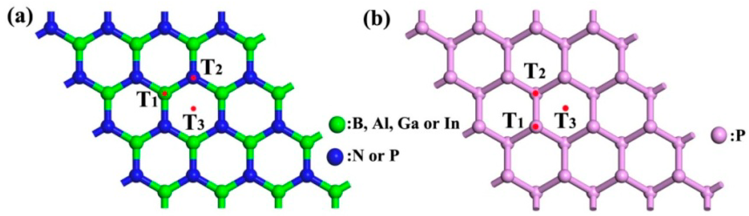
2. Materials and Methods

All the calculations related to the interactions between CH2O and the monolayer substrates (i.e., BN, AlN, GaN, InN, BP, and P) were performed based on density functional theory (DFT) [30], using the Dmol3 package [31]. The generalized gradient approximation was performed using the Perdew–Burke–Ernzerhof (PBE) method [32]. For geometry optimizations, the convergence thresholds for displacement, energy gradient, and energy were considered to be 5 × 10⁻³ Å, 2 × 10⁻³ Ha/Å, and 1 × 10⁻⁵ Ha, respectively. While investigating the CH2O adsorption, the van der Waals interaction was considered to be critical. Hence, the method of Grimme [33] was employed while performing all the calculations. Furthermore, the Monkhorst–Pack mesh of 12 × 12 × 1 was selected for calculating the electronic structures. The gas adsorption system comprised a 4 × 4 supercell and one CH2O molecule inside, in which a vacuum of 25 Å was constructed.
To evaluate the gas adsorption strength between these monolayer materials and the gas molecules, the gas adsorption energy was defined as
Ea = E(sub+molecule)EmoleculeEsub
where E(sub+molecule), Emolecule, and Esub denote the total energies of the adsorption system, CH2O, and substrate, respectively. Further, the charge density difference was calculated as
Δρ = ρ(sub+molecule)ρmoleculeρsub
where ρ(sub+molecule), ρmolecule, and ρsub denote the total charge densities of the adsorption system, CH2O, and substrate, respectively. Furthermore, the charge transfer (Q) was calculated using the Hirshfeld method, and the adsorption distance (d) was also calculated. The negative value of Q indicates that the CH2O molecule collects the electrons from the substrate, whereas d denotes the nearest distance between the substrate and the CH2O molecule.

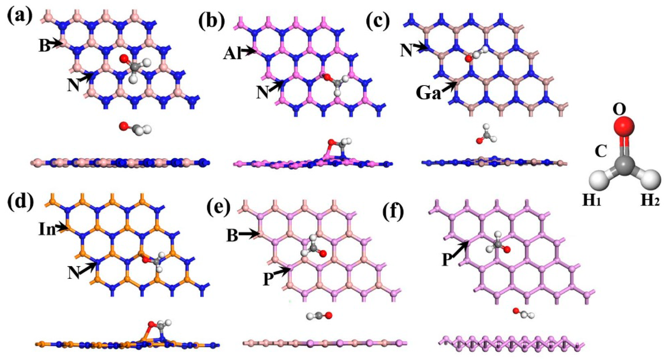
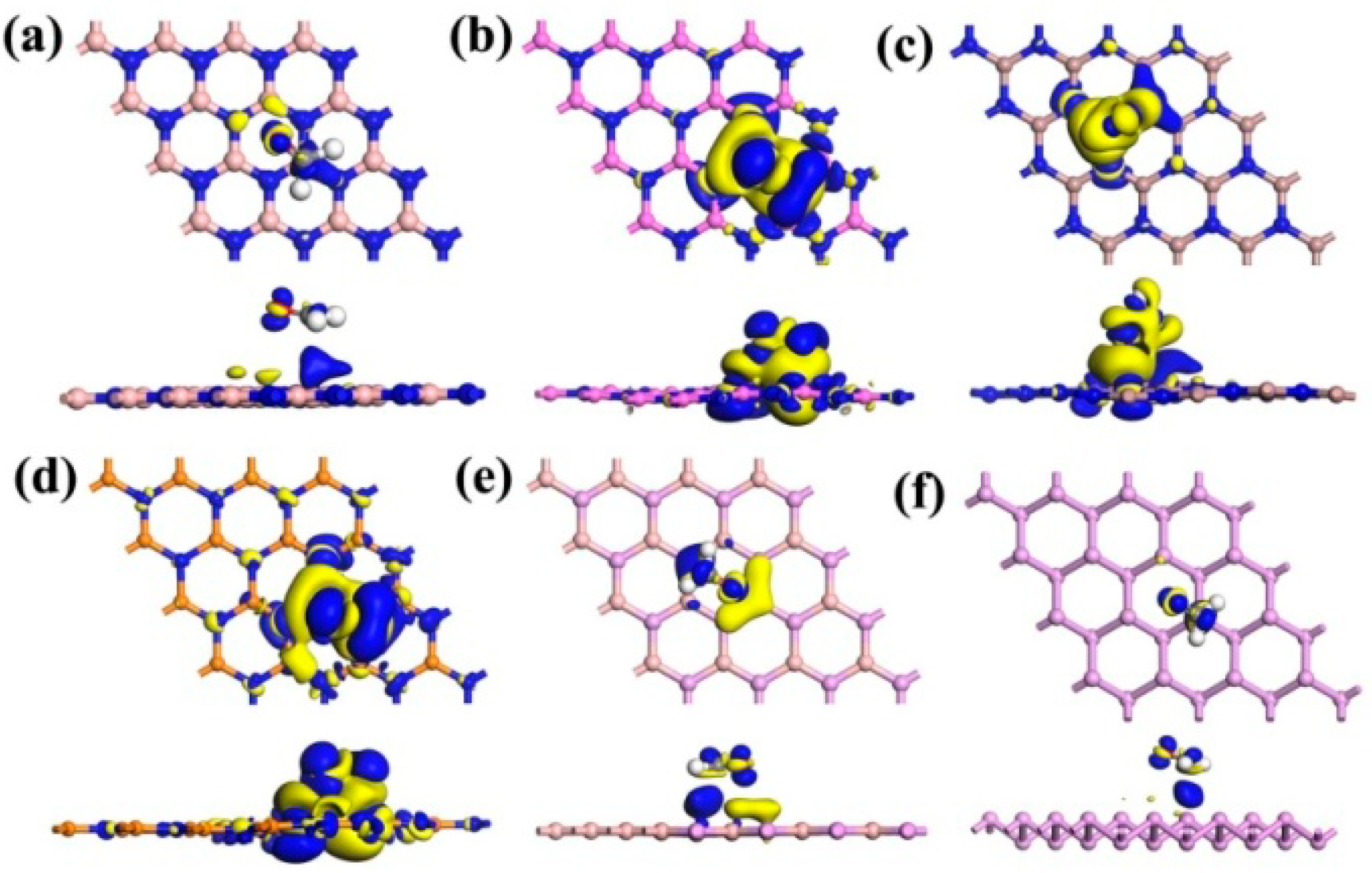
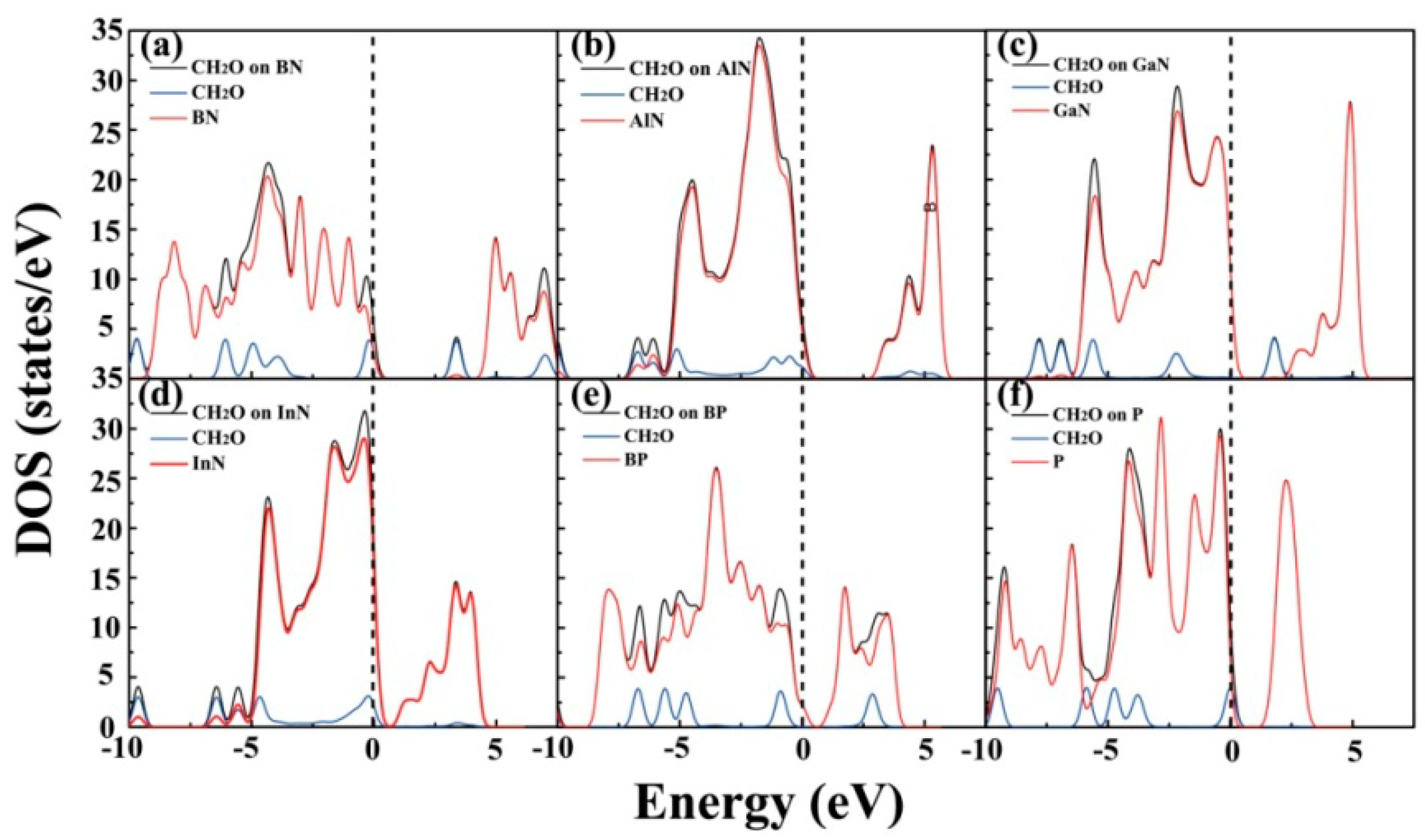
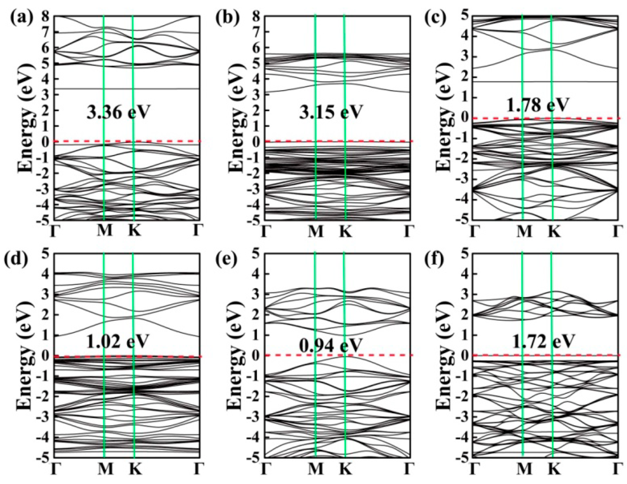
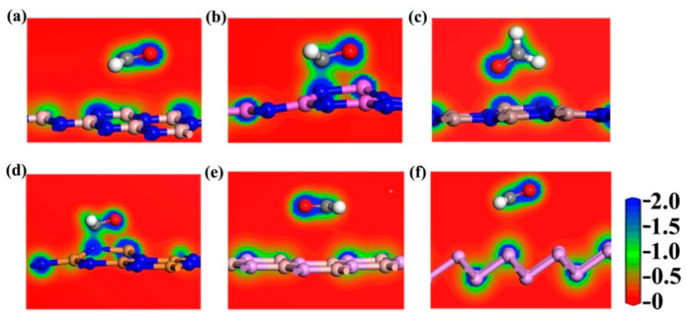
3. Results and Discussion

The structures of the BN, AlN, GaN, InN, BP, and P monolayers are 4 × 4 supercells, and the lattice parameters of the primary cells are 2.51, 3.13, 3.21, 3.63, 3.21, and 3.31 Å, respectively. The calculations of our structural constants were observed to be in good agreement with those of others [4,6,7,8,13,34]. While determining the most stable structures of CH2O on the BN, AlN, GaN, InN, and BP surfaces, three representative initial sites, including the top of X (herein after referred to as B, Al, Ga, In, and B) atoms (T1), top of N or P atoms (T2), and top of hexagon centers (T3) were considered, as plotted in Figure 1a. For the P monolayer three representative initial sites were calculated, as depicted in Figure 1b. After structural optimization, the most stable adsorption structures for CH2O on the surface of the BN, AlN, GaN, InN, BP, and P monolayers could be selected by choosing the lowest E(sub+molecule) of the three initial adsorption positions T1–T3, as depicted in Figure 2. In the BN, AlN, GaN, and InN, monolayers, CH2O tended to be adsorbed on the top of B, Al, Ga, and In, respectively. After the gas adsorption of CH2O, the structures of AlN, GaN, and InN exhibited various deformation levels, whereas no obvious deformation was observed in the BN, BP, and P structures. In the subsequent discussion, all the results were calculated using these stable structures.
The calculated values of Ea, Q, and d for the most energetically stable adsorption structures are presented in Table 1. For CH2O on the surface of the BN, GaN, BP, and P monolayers, the values of Ea were −0.283, −0.456, −0.249, and −0.188 eV, respectively. Furthermore, the values of Ea for CH2O on the surface of pristine graphene was −0.162 eV [29], indicating that CH2O was easier to adsorb on the aforementioned materials than pristine graphene. The calculated values of d for BN, GaN, BP, and P were 2.990, 2.361, 3.328, and 3.230 Å, respectively, which were considerably larger than the bond length between the atom in CH2O and the substrate (i.e., lH–N = 1.03 Å, lO–Ga = 1.87 Å, lO–B = 1.48 Å, and lC–P = 1.38 Å, respectively) [35]. Thus, the adsorption of CH2O on these materials was considered to exhibit the trends of physical adsorption. The Ea values for CH2O on the AlN and InN surfaces were −1.044 and −1.046 eV, respectively, which were considerably larger than those of other materials. Meanwhile, the adsorption distances were 1.566 and 1.555 Å, respectively, which were in the bonding range (lC–N = 1.46 Å), indicating that chemical adsorption may be observed in these two cases.
Previous studies related to the (indium selenide) InSe and BP monolayers have demonstrated that the resistivity of the substrate can be altered by the adsorbed gas molecules using the charge transfer mechanism, implying that the value of Q plays an important role in the gas adsorption behavior [25,36]. The calculated values of Q for the CH2O adsorbed on the BN, AlN, GaN, InN, BP, and P monolayers were −0.019, −0.206, −0.107, −0.319, −0.065, and −0.067 e, respectively, revealing that the CH2O molecule gained electrons from these substrates. The Q values of the CH2O adsorbed on pristine graphene [29] and MoS2 [28] were −0.008 and −0.010 e, respectively, indicating that the charge transfers between CH2O and these materials were more noticeable than that to pristine MoS2 or graphene. To further investigate the charge transfers between CH2O and the substrates, the charge density differences were calculated, where the blue region represents an increase in the number of electrons, whereas the yellow region indicates electron reduction, as depicted in Figure 3. For CH2O on the surface of the AlN, GaN, and InN monolayers yellow regions were observed to be localized around the substrates, indicating that CH2O obtains electrons from the substrates. However, for CH2O on the surface of the BN, BP, and P monolayers, the blue or yellow regions were observed to be small, and the absolute values of Q were smaller than 0.07 e. These results indicate that the charge transfer in these cases was less evident when compared with that observed in case of the aforementioned materials (i.e., AlN, GaN, and InN). The charge transfers were reported to alter the number of charge carriers and resistance of the substrate [20]. Thus, the resistance of AlN, GaN, and InN may be noticeably altered after the adsorption of CH2O.
To perform an in-depth investigation of the adsorption of CH2O on the BN, AlN, GaN, InN, BP, and P monolayers, the density of states (DOSs) for the CH2O substrate systems were calculated, as depicted in Figure 4. Notably, for all the adsorption systems, the contribution of the electronic levels of CH2O was observed between −2.5 and 2.5 eV, which is around the Fermi level (Ef). Note that the DOSs near Ef may exhibit a remarkable effect on the electronic characteristics of materials [3,22]. Thus, the existence of CH2O may have different degrees of influence on the electronic properties of these materials. To perform an in-depth investigation into the effects of CH2O on the electronic characteristics of the substrate, the band structures were also calculated, as shown in Figure 5. The band structure is an important parameter for determining the electrical properties of materials [24]. The band gaps of CH2O adsorbed on the BN, AlN, GaN, InN, BP, and P monolayers were 3.36, 3.15, 1.78, 1.02, 0.94, and 1.72 eV, respectively. The band gaps of pure substrates were as follows: Eg–BN = 4.67 eV; Eg–AlN = 3.43 eV; Eg–GaN = 2.45 eV; Eg–InN = 0.83 eV; Eg–BP = 0.94 eV; and Eg–P = 1.97 eV (refer to Figure S1 of “Supplementary Materials”). This result implies that the adsorption of CH2O had a noticeable effect on the electrical characteristics of these monolayer materials, except for BP. Because of the large band gap, BN is an insulator and not suitable for application in gas sensors. For CH2O on the surface of the P monolayer, the Ea and Q values were quite small even though CH2O influenced the electronic characteristics of the monolayer. This result indicates that P was not the most suitable material for detecting CH2O in our study. The AlN, GaN, and InN monolayers may have excellent potential for the detection of CH2O.
To obtain detailed confirmation about the type of gas adsorption behavior, the total electronic densities were also calculated, as depicted in Figure 6. The slices of electronic densities can help to determine the occurrence of a new chemical bonding. For instance, when CH2O is adsorbed on the BN monolayer, no obvious charge distribution was observed between the CH2O and BN atoms, and the adsorption distance was 2.99 Å, implying that the type of gas adsorption behavior was physical adsorption. Similarly, the gas adsorption behavior types of CH2O adsorbed on the GaN, BP, and P monolayers were also observed to follow the trend of physical adsorption. In the case of CH2O on the AlN and InN surfaces, the charge distribution between the CH2O and the substrates were apparent, considering the small adsorption distances, considerable adsorption energies, and large charge transfers, revealing the formation of new covalent bonds. As previously mentioned, the gas adsorption of CH2O was observed to noticeably influence the electrical properties of the AlN, InN and GaN monolayers. Given that the gas adsorption types of CH2O on the AlN and InN surfaces followed the trend of chemical adsorption, they exhibit an excellent potential for catalyzing CH2O or as disposable gas sensors for CH2O detection. For CH2O on the GaN surface, a chemical bond was observed between the gas molecule and the substrate. CH2O was therefore easily desorbed from the GaN monolayer after adsorption. Moreover, compared with In, the resources of Ga in China, USA, and the EU are considerable [17], indicating that GaN is suitable for use in gas sensors for CH2O detection.

4. Conclusions

In summary, the structure, charge transfers, and electronic characteristics of CH2O adsorbed on the BN, AlN, GaN, InN, BP, and P monolayers were investigated using first-principles calculations. For the adsorption of CH2O on the BN, GaN, BP, and P surfaces, the gas adsorption behavior followed the trends of physical adsorption. By assessing the band structures and DOSs of the gas adsorption systems, it was found that the electronic characteristics of these materials was evidently altered by the adsorption of the CH2O molecule, except for the BP monolayer. The GaN monolayer was considered to be the most suitable material for detecting CH2O in our study because of its appreciable charge transfer and moderate adsorption energy. The adsorption of CH2O on the surface of the AlN and InN monolayers was observed to follow the trends of chemical adsorption, with large charge transfers and considerable adsorption energies, revealing that AlN and InN have excellent potential for catalyzing CH2O or in disposable gas sensors for CH2O detection.

Supplementary Materials

The following are available online at https://www.mdpi.com/1996-1944/12/4/676/s1, Figure S1: Band structures of pristine (a) BN, (b) AlN, (c) GaN, (d) InN, (e) BP, and (f) P. monolayers.

Author Contributions

H.Q. and C.F. conceived this research; C.F. and H.Q. carried out the calculations; C.F. and H.Q. designed and wrote the article; D.Y. and G.Z. reviewed the article. All authors read and approved the final manuscript.

Funding

Our investigation was sponsored by Guangxi Natural Science Foundation under grant Nos. 2016GXNSFBA380114 and 2018GXNSFAA281222, Guangxi Thousand Talents Training Plan of Middle-Aged and Young Backbone Teacher (Hongbo Qin), and the Innovation Project of GUET Graduate Education under grant No. 2018YJCX04.

Conflicts of Interest

The authors declare no conflict of interest.

References

  1. Chhowalla, M.; Jena, D.; Zhang, H. Two-dimensional semiconductors for transistors. Nat. Rev. Mater. 2016, 1, 16052. [Google Scholar] [CrossRef]
  2. Bonaccorso, F.; Sun, Z.; Hasan, T.; Ferrari, A.C. Graphene photonics and optoelectronics. Nat. Photonics 2016, 4, 611–622. [Google Scholar] [CrossRef]
  3. Meng, R.S.; Cai, M.; Jiang, J.K.; Liang, Q.H.; Sun, X.; Yang, Q.; Tan, C.J.; Chen, X.P. First principles investigation of small molecules adsorption on Antimonene. IEEE Electron Device Lett. 2017, 38, 134–137. [Google Scholar] [CrossRef]
  4. Topsakal, M.; Aktürk, E.; Ciraci, S. First-principles study of two-and one-dimensional honeycomb structures of boron nitride. Phys. Rev. B 2009, 79, 115442. [Google Scholar] [CrossRef]
  5. Gibaja, C.; Rodriguez-San-Miguel, D.; Ares, P.; Gómez-Herrero, J.; Varela, M.; Gillen, R.; Maultzsch, J.; Hauke, F.; Hirsch, A.; Abellán, G. Few-layer antimonene by liquid-phase exfoliation. Angew. Chem. Int. Ed. 2016, 55, 14345–14349. [Google Scholar] [CrossRef] [PubMed]
  6. Bacaksiz, C.; Sahin, H.; Ozaydin, H.; Horzum, S.; Senger, R.T.; Peeters, F.M. Hexagonal AlN: Dimensional-crossover-driven band-gap transition. Phys. Rev. B 2015, 91, 085430. [Google Scholar] [CrossRef] [Green Version]
  7. Onen, A.; Kecik, D.; Durgun, E.; Ciraci, S. GaN: From three- to two-dimensional single-layer crystal and its multilayer van der Waals solids. Phys. Rev. B 2016, 93, 085431. [Google Scholar] [CrossRef]
  8. Dan, L.; Quhe, R.; Chen, Y.; Wu, L.; Qian, W.; Guan, P.; Wang, S.; Lu, P. Electronic and excitonic properties of two-dimensional and bulk InN crystals. RSC Adv. 2017, 7, 42455–42461. [Google Scholar] [Green Version]
  9. Angshuman, N.; Kalyan, R.; Hembram, K.P.S.S.; Ranjan, D.; Waghmare, U.V.; Rao, C.N.R. Graphene analogues of BN: novel synthesis and properties. ACS Nano 2010, 4, 1539–1544. [Google Scholar]
  10. Tsipas, P.; Kassavetis, S.; Tsoutsou, D.; Xenogiannopoulou, E.; Golias, E.; Giamini, S.A.; Grazianetti, C.; Chiappe, D.; Molle, A.; Fanciulli, M.; et al. Evidence for graphite-like hexagonal AlN nanosheets epitaxially grown on single crystal Ag(111). Appl. Phys. Lett. 2013, 103, 251605. [Google Scholar] [CrossRef]
  11. Chen, Y.; Liu, K.; Liu, J.; Lv, T.; Wei, B.; Zhang, T.; Zeng, M.; Wang, Z.; Fu, L. Growth of 2D GaN single crystals on liquid metals. J. Am. Chem. Soc. 2018, 140, 16392–16395. [Google Scholar] [CrossRef] [PubMed]
  12. Xu, H.; Liu, Z.; Zhang, X.; Hark, S. Synthesis and optical properties of InN nanowires and nanotubes. Appl. Phys. Lett. 2007, 90, 113105. [Google Scholar] [CrossRef]
  13. Çakır, D.; Kecik, D.; Sahin, H.; Durgun, E.; Peeters, F.M. Realization of a p-n junction in a single layer boron-phosphide. Phys. Chem. Chem. Phys. 2015, 17, 13013–13020. [Google Scholar] [CrossRef] [PubMed]
  14. Li, G.; Abbott, J.K.C.; Brasfield, J.D.; Liu, P.; Dale, A.; Duscher, G.; Rack, P.D.; Feigerle, C.S. Structure characterization and strain relief analysis in CVD growth of boron phosphide on silicon carbide. Appl. Surf. Sci. 2015, 327, 7–12. [Google Scholar] [CrossRef] [Green Version]
  15. Zhang, J.L.; Zhao, S.; Han, C.; Wang, Z.; Zhong, S.; Sun, S.; Guo, R.; Zhou, X.; Gu, C.D.; Yuan, K.D. Epitaxial growth of single layer blue phosphorus: a new phase of two-dimensional phosphorus. Nano Lett. 2016, 16, 4903–4908. [Google Scholar] [CrossRef] [PubMed]
  16. Xie, J.; Si, M.; Yang, D.; Zhang, Z.; Xue, D. A theoretical study of blue phosphorene nanoribbons based on first-principles calculations. J. Appl. Phys. 2014, 116, 073704. [Google Scholar] [CrossRef] [Green Version]
  17. EU Commission. Study on the Review of the List of Critical Raw Materials; European Commission: Brussels, Belgium, 2017; Available online: https://publications.europa.eu/publication-detail/-/publication/08fdab5f-9766-11e7-b92d-01aa75ed71a1/language-en (accessed on 10 February 2019). [CrossRef]
  18. Yuan, W.; Shi, G. Graphene-based gas sensors. J. Mater. Chem. A 2013, 1, 10078–10091. [Google Scholar] [CrossRef]
  19. Liu, N.; Zhou, S. Gas adsorption on monolayer blue phosphorus: Implications for environmental stability and gas sensors. Nanotechnology 2017, 28, 175708–175726. [Google Scholar] [CrossRef] [PubMed]
  20. Qu, Y.; Shao, Z.; Chang, S.; Li, J. Adsorption of gas molecules on monolayer MoS2 and effect of applied electric field. Nanoscale Res. Lett. 2013, 8, 425. [Google Scholar]
  21. Lin, L.; Liu, T.; Yu, Z.; Rong, S.; Wen, Z.; Wang, Z. Synthesis of boron nitride nanosheets with a few atomic layers and their gas-sensing performance. Ceram. Int. 2015, 42, 971–975. [Google Scholar] [CrossRef]
  22. Wang, Y.; Song, N.; Song, X.; Zhang, T.; Meng, L. A first-principles study of gas adsorption on monolayer AlN sheet. Vacuum 2018, 147, 18–23. [Google Scholar] [CrossRef]
  23. Yong, Y.; Cui, H.; Zhou, Q.; Su, X.; Kuang, Y.; Li, X. Adsorption of gas molecules on a graphitic GaN sheet and its implications for molecule sensors. RSC Adv. 2017, 7, 51027–51035. [Google Scholar] [CrossRef] [Green Version]
  24. Sun, X.; Yang, Q.; Meng, R.S.; Tan, C.J.; Liang, Q.H.; Jiang, J.K.; Ye, H.Y.; Chen, X.P. Adsorption of gas molecules on graphene-like InN monolayer: A first-principle study. Appl. Surf. Sci. 2017, 404, 291–299. [Google Scholar] [CrossRef]
  25. Cheng, Y.F.; Meng, R.S.; Tan, C.J.; Chen, X.P.; Xiao, J. Selective gas adsorption and I-V response of monolayer boron phosphide introduced by dopants: A first-principle study. Appl. Surf. Sci. 2018, 427, 176–188. [Google Scholar] [CrossRef]
  26. Ning, H.; Tian, Y.; Wu, X.; Chen, Y. Improving humidity selectivity in formaldehyde gas sensing by a two-sensor array made of Ga-doped ZnO. Sens. Actuators B-Chem. 2009, 138, 228–235. [Google Scholar]
  27. Lee, C.Y.; Chiang, C.M.; Wang, Y.H.; Ma, R.H. A self-heating gas sensor with integrated NiO thin-film for formaldehyde detection. Sens. Actuators B-Chem. 2007, 122, 503–510. [Google Scholar] [CrossRef]
  28. Ma, D.; Ju, W.; Li, T.; Gui, Y.; He, C.; Ma, B.; Tang, Y.; Lu, Z.; Yang, Z. Formaldehyde molecule adsorption on the doped monolayer MoS2: A first-principles study. Appl. Surf. Sci. 2016, 371, 180–188. [Google Scholar] [CrossRef]
  29. Chen, X.; Xu, L.; Liu, L.L.; Zhao, L.S.; Chen, C.P.; Zhang, Y.; Wang, X.C. Adsorption of formaldehyde molecule on the pristine and transition metal doped graphene: First-principles study. Appl. Surf. Sci. 2017, 396, 1020–1025. [Google Scholar] [CrossRef]
  30. Kohn, W.; Sham, L.J. Self-consistent equations including exchange and correlation effects. Phys. Rev. 1965, 140, A1133–A1138. [Google Scholar] [CrossRef]
  31. Delley, B. From molecules to solids with the DMol3 approach. J. Chem. Phys. 2000, 113, 7756–7764. [Google Scholar] [CrossRef]
  32. Perdew, J.P.; Burke, K.; Ernzerhof, M. Generalized gradient approximation made simple. Phys. Rev. Lett. 1996, 77, 3865–3868. [Google Scholar] [CrossRef] [PubMed]
  33. Grimme, S. A consistent and accurate ab initio parametrization of density functional dispersion correction (DFT-D) for the 94 elements H-Pu. J. Chem. Phys. 2010, 132, 154104. [Google Scholar] [CrossRef] [PubMed]
  34. Zhu, Z.; Tománek, D. Semiconducting layered blue phosphorus: A computational study. Phys. Rev. Lett. 2014, 112, 176802–176805. [Google Scholar] [CrossRef] [PubMed]
  35. Pyykkö, P.; Atsumi, M. Molecular single-bond covalent radii for elements 1-118. Chem.-Eur. J. 2009, 15, 186–197. [Google Scholar] [CrossRef] [PubMed]
  36. Ma, D.W.; Ju, W.W.; Tang, Y.N.; Chen, Y. First-principles study of the small molecule adsorption on the InSe monolayer. Appl. Surf. Sci. 2017, 426, 244–252. [Google Scholar] [CrossRef]
Figure 1. Three representative initial adsorption sites for (a) boron nitride (BN), (aluminum nitride) AlN, (gallium nitride) GaN, (indium nitride) InN, and boron phosphide (BP) and for (b) phosphorus (P).
Materials 12 00676 g001
Figure 2. Most stable adsorption structures of CH2O on the surface of the (a) BN, (b) AlN, (c) GaN, (d) InN, (e) BP, and (f) P monolayers.
Materials 12 00676 g002
Figure 3. Charge density differences for the CH2O adsorbed on the surface of the (a) BN, (b) AlN, (c) GaN, (d) InN, (e) BP, and (f) P monolayers with an isosurface value of 0.003 e/Å3. The blue and yellow contours denote the increase and decrease of electrons, respectively.
Materials 12 00676 g003
Figure 4. Density of states (DOSs) of CH2O on the surface of the (a) BN, (b) AlN, (c) GaN, (d) InN, (e) BP, and (f) P monolayers.
Materials 12 00676 g004
Figure 5. Band structures of CH2O on the surface of the (a) BN, (b) AlN, (c) GaN, (d) InN, (e) BP, and (f) P monolayers.
Materials 12 00676 g005
Figure 6. Slices of charge densities for the CH2O adsorbed on the (a) BN, (b) AlN, (c) GaN, (d) InN, (e) BP, and (f) P monolayers. The charge density ranges from 0 to 2 e/A3.
Materials 12 00676 g006
Table 1. Ea, Q, and d of the gas adsorption systems of CH2O adsorbed on the BN, AlN, GaN, InN, BP, and P monolayers.
SubstrateSiteEa (eV)Q (e)d (Å)
BNT1−0.283−0.0192.990 (H–N)
AlNT1−1.044−0.2061.566 (C–N)
GaNT1−0.456−0.1072.361 (O–Ga)
InNT1−1.046−0.3191.555 (C–N)
BPT3−0.249−0.0653.328 (O–B)
PT1−0.188−0.0673.230 (C–P)

