Structural and Optical Characterization of ZnS Ultrathin Films Prepared by Low-Temperature ALD from Diethylzinc and 1.5-Pentanedithiol after Various Annealing Treatments

 , , , ,

Abstract
1. Introduction
2. Materials and Methods
- β—integral breadth, depending on crystallite size and microstrain (in radians);
- ϴ—Bragg angle (in radians);
- K—shape factor (dimensionless);
- λ—wavelength of the X-ray (in Angstrom);
- D—crystallite size (in Angstrom);
- ε—microstrain (.
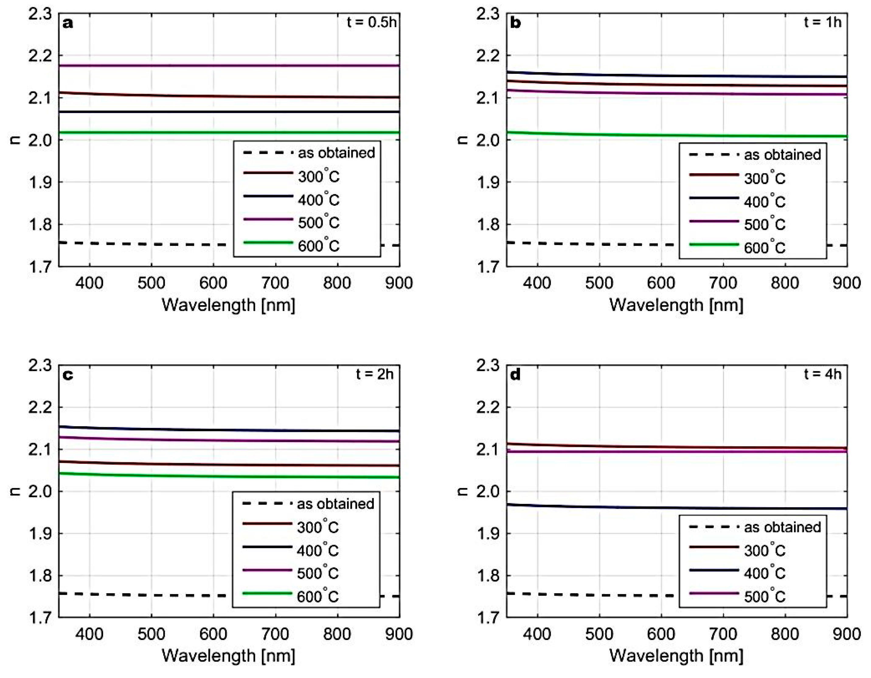
3. Results and Discussion
4. Conclusions
Supplementary Materials
Author Contributions
Funding
Conflicts of Interest
References
- Xiong, Q.; Chen, G.; Acord, J.D.; Liu, X.; Zengel, J.J.; Gutierrez, H.R.; Redwing, J.M.; Lew Yan Voon, L.C.; Lassen, B.; Eklund, P.C. Optical properties of rectangular cross-sectional ZnS nanowires. Nano Lett. 2004, 4, 1663–1668. [Google Scholar] [CrossRef]
- Fang, X.; Wu, L.; Hu, L. ZnS nanostructure arrays: A developing material star. Adv. Mater. 2011, 23, 585–598. [Google Scholar] [CrossRef] [PubMed]
- Zhang, H.; Chen, X.; Li, Z.; Kou, J.; Yu, T.; Zou, Z. Preparation of sensitized ZnS and its photocatalytic activity under visible light irradiation. J. Phys. D Appl. Phys. 2007, 40, 6846–6849. [Google Scholar] [CrossRef]
- Ruffner, J.A.; Hilmel, M.D.; Mizrahi, V.; Stegeman, G.I.; Gibson, U. Effects of low substrate temperature and ion assisted deposition on composition, optical properties, and stress of ZnS thin films. J. Appl. Opt. 1989, 28, 5209–5214. [Google Scholar] [CrossRef] [PubMed]
- Elidrissi, B.; Addou, M.; Regragui, M.; Bougrine, A.; Kachouane, A.J.; Bernède, C. Structure, composition and optical properties of ZnS thin films prepared by spray pyrolysis. Mater. Chem. Phys. 2001, 68, 175–179. [Google Scholar] [CrossRef]
- Bhan, R.K.; Srivastava, V.; Saxena, R.S.; Sareen, L.; Pal, R.; Sharma, R.K. Improved high resistivity ZnS films on HgCdTe for passivation of infrared devices. Infrared Phys. Technol. 2010, 53, 404–409. [Google Scholar] [CrossRef]
- Sun, C.H.; Zhang, P.; Zhang, T.N.; Chen, X.; Chen, Y.Y.; Ye, Z.H. ZnS thin films grown by atomic layer deposition on GaAs and HgCdTe substrates at very low temperature. Infrared Phys. Technol. 2017, 85, 280–286. [Google Scholar] [CrossRef]
- Pacheco, M.E.; Castells, C.B.; Bruzzone, L. Mn-doped ZnS phosphorescent quantum dots: Coumarins optical sensors. Sens. Actuators B Chem. 2017, 238, 660–666. [Google Scholar] [CrossRef]
- Liu, X.; Yang, Y.; Li, Q.; Wang, Z.; Xing, X.; Wang, Y. Portably colorimetric paper sensor based on ZnS quantum dots for semi-quantitative detection of Co2+ through the measurement of grey level. Sens. Actuators B Chem. 2018, 260, 1068–1075. [Google Scholar] [CrossRef]
- Borgohain, R.; Boruah, P.K.; Baruah, S. Heavy-metal ion sensor using capped ZnS quantum dots. Sens. Actuators B Chem. 2016, 226, 534–539. [Google Scholar] [CrossRef]
- Wu, D.; Chen, Z. ZnS quantum dots as pH probes for study of enzyme reaction kinetics. Enzym. Microb. Technol. 2012, 51, 47–52. [Google Scholar] [CrossRef] [PubMed]
- Mobarraz, M.; Ganjali, M.R.; Chaichi, M.J.; Norouzi, P. Functionalized ZnS quantum dots as luminescent probes for detection of amino acids. Spectrochim. Acta Part A Mol. Biomol. Spectrosc. 2012, 96, 801–804. [Google Scholar] [CrossRef] [PubMed]
- Johnson, R.W.; Hultqvist, A.; Bent, S.F. A brief review of atomic layer deposition: From fundaments to applications. Mater. Today 2015, 17, 236–246. [Google Scholar] [CrossRef]
- Knez, M.; Nielsch, K.; Niinisto, L. Synthesis and Surface engineering of complex nanostructures by atomic layer deposition. Adv. Mater. 2007, 19, 3425–3438. [Google Scholar] [CrossRef]
- Ahvenniemi, E.; Akbashev, A.R.; Ali, S.; Bechelany, M.; Berdova, M.; Boyadjiev, S.; Cameron, D.C.; Chen, R.; Chubarov, M.; Cremers, V.; et al. Review article: Recommended reading list of early publications on atomic layer deposition—Outcome of the „Virtual Project on the History of ALD”. J. Vac. Sci. Technol. A 2017, 35, 10801. [Google Scholar] [CrossRef]
- Szczerbakow, A.; Dynowska, E.; Godlewski, M.; Świątek, K. Monocrystalline ZnS-sphalerite films grown by atomic layer epitaxy in a gas flow system. J. Cryst. Growth 1998, 183, 708–710. [Google Scholar] [CrossRef]
- Yun, S.J.; Dey, S.; Nam, K.S. Zinc sulfide and terbium-doped zinc sulfide films grown by traveling wave reactor atomic layer epitaxy. J. Korean Phys. Soc. 1998, 33, S454–S457. [Google Scholar]
- Wu, Y.-H.; Toyoda, T.; Kawakami, Y.; Fujita, S. Atomic layer epitaxy of ZnS on GaAs substrates by metalorganic molecular beam epitaxy. Jpn. J. Appl. Phys. 1990, 29, L727–L730. [Google Scholar] [CrossRef]
- Hsu, C.T. Epitaxial growth of II-VI compound semiconductors by atomic layer epitaxy. Thin Solid Film 1998, 335, 284–291. [Google Scholar] [CrossRef]
- Kim, Y.S.; Yun, S.J. Studies on polycrystalline ZnS thin films grown by atomic layer deposition for electroluminescent applications. Appl. Surf. Sci. 2004, 229, 105–111. [Google Scholar] [CrossRef]
- Yokoyama, M.; Chen, N.-T. ALE growth and optical characterization of ZnSe/ZnS strained quantum well structures on Si substrate. J. Cryst. Growth 2001, 223, 369–375. [Google Scholar] [CrossRef]
- Tanskanen, J.T.; Bakke, J.R.; Bent, S.F.; Pakkanen, T.A. ALS growth characteristics of ZnS films deposited from organozinc and hydrogen sulfide precursors. Langmuir 2010, 26, 11899–11906. [Google Scholar] [CrossRef] [PubMed]
- Xu, R.; Takoudis, C.G. Chemical passivation of GaSb-based surfaces by atomic layer depostied ZnS using diethyzinc and hydrogen sulfide. J. Vac. Sci. Technol. A 2012, 30, 1A145. [Google Scholar] [CrossRef]
- Bakke, J.R.; King, J.S.; Jung, H.J.; Sinclair, R.; Bent, S.F. Atomic layer deposition of ZnS via in situ production of H2S. Thin Solid Film 2010, 518, 5400–5408. [Google Scholar] [CrossRef]
- Miikkulainen, V.; Leskelä, M.; Ritala, M.; Puurunen, R.L. Crystallinity of inorganic films grown by atomic layer deposition: Overview and general trends. J. Appl. Phys. 2013, 113, 21301. [Google Scholar] [CrossRef]
- Ko, D.-H.; Kim, S.; Jin, Z.; Shin, S.; Lee, S.Y.; Min, Y.-S. A novel chemical route to atomic layer deposition of ZnS thin film from Diethylzinc and 1,5-Pentanedithiol. Bull. Korean Chem. Soc. 2017, 38, 696–699. [Google Scholar] [CrossRef]
- Lahtinen, J.A.; Lu, A.; Tuomi, T.; Tammenmaa, M. Effect of growth temperature on the electronic energy band and crystal structure of ZnS thin films grown using atomic layer epitaxy. J. Appl. Phys. 1985, 58, 1851–1853. [Google Scholar] [CrossRef]
- Putkonen, M.; Sajavaara, T.; Niinistö, L.; Keinonen, J. Analysis of ALD-processed thin films by ion-beam techniques. Anal. Bioanal. Chem. 2005, 382, 1791–1799. [Google Scholar] [CrossRef]
- Whitlow, H.J.; Possnert, G.; Petersson, C.S. Quantitative mass and energy dispersive elastic recoil spectrometry: Resolution and efficiency consideration. Nucl. Instrum. Meth. B 1987, 27, 448–457. [Google Scholar] [CrossRef]
- Ziegler, J.F. SRIM. Available online: http://www.SRIM.org, (accessed on 29 April 2019).
- Izumi, F.; Ikeda, T. Implementation of the Williamson-Hall and Halder-Wagner Methods into RIETAN-FP. Ann. Rep. Adv. Ceram. Res. Center Nagoya Inst. Technol. 2015, 3, 33–38. [Google Scholar]
- Tompkins, H.G.; Irene, E.A. Handbook of Ellipsometry; William Andrew Inc.: Norwich, UK, 2005. [Google Scholar]
- Dutková, E.; Daneu, N.; Lukáčová Bujňáková, Z.; Baláž, M.; Kováč, J.; Baláž, P. Mechanochemical synthesis and characterization of CuInS2/ZnS nanocrystals. Molecules 2019, 24, 1031. [Google Scholar] [CrossRef] [PubMed]
- Nitta, E.; Kimata, M.; Hoshino, M.; Echigo, T.; Hamasaki, S.; Nishida, N.; Shimizu, M.; Akasaka, T. Crystal chemistry of ZnS minerals formed as high-temperature volcanic sublimates: Matraite identical with sphalerite. J. Miner. Petrol. Sci. 2008, 103, 145–151. [Google Scholar] [CrossRef][Green Version]
- Terohid, S.A.A.; Heidari, S.; Jafari, A.; Asgary, S. Effect of growth time on structural, morphological and electrical properties of tungsten oxide nanowire. Appl. Phys. A 2018, 124, 567. [Google Scholar] [CrossRef]
- Frentrup, M.; Lee, S.-L.; Sahonta, L.Y.; Kappers, M.J.; Massabuau, F.; Gupta, P.; Oliver, R.A.; Humphreys, C.J.; Wallis, D.J. X-ray diffraction analysis of cubic zincblende III-nitrides. J. Phys. D Appl. Phys. 2017, 50, 433002. [Google Scholar] [CrossRef]
- Tafwidli, F.; Kang, Y.-B. Thermodynamic modeling of Fe-C-S ternary system. ISIJ Int. 2017, 57, 782–790. [Google Scholar] [CrossRef]
- Sharma, R.C.; Chang, Y.A. The S-Zn (sulfur-zinc) system. J. Phase Equilibr. 1996, 17, 261–266. [Google Scholar] [CrossRef]
- MTDATA—Phase Diagram Software from the National Physical Laboratory. Available online: http://resource.npl.co.uk/mtdata/phdiagrams/czn.htm (accessed on 29 April 2019).
- Kim, K.-H.; Park, Q.-H. Maximal light-energy transfer through a dielectric/metal-layered electrode on a photoactive device. Opt. Express 2014, 22, 1963–1970. [Google Scholar] [CrossRef]
- Zakerian, F.; Kafashan, H. Investigation the effect of annealing parameters on the physical properties of electrodeposited ZnS thin films. Superlattices Microstruct. 2018, 124, 92–106. [Google Scholar] [CrossRef]
- Kedawat, G.; Kumar, P.; Vijay, Y.K.; Gupta, B.K. Fabrication of highly efficient resonant structure assisted ultrathin artificially stacked Ag/ZnS/Ag multilayer films for color filter applications. J. Mater. Chem. C 2015, 3, 6745–6754. [Google Scholar] [CrossRef]
- Liu, X.; Cai, X.; Qiao, J.; Mao, J.; Jiang, N. The design of ZnS/Ag/ZnS transparent conductive multilayer films. Thin Solid Film 2003, 441, 200–206. [Google Scholar] [CrossRef]
- Nouri, H.; Cadiou, C.; Lawson-Daku, L.M.; Hauser, A.; Chevreux, S.; Déchamps-Olivier, I.; Lachaud, F.; Ternane, R.; Trabelsi-Ayadi, M.; Chuburua, F.; et al. A modified cyclen azaxanthone ligand as a new fluorescent probe for Zn 2+. Dalton Trans. 2013, 42, 12157–12164. [Google Scholar] [CrossRef] [PubMed]
- Mahiuddin, M.D.; Banerjee, M.; Shaikh, A.; Shyam, T.; Taniya, S.; Ghosh, A.; Adhikary, A.; Brandao, P.; Felix, V.; Das, D. Optical sensors for detection of nano-molar Zn2+ in aqueous medium: Direct evidence of probe- Zn2+ binding by single crystal X-ray structures. J. Photochem. Photobiol. A Chem. 2019, 368, 52–61. [Google Scholar] [CrossRef]
- Wu, W.-N.; Mao, P.-D.; Wang, Y.; Zhao, X.-L.; Xu, Z.-Q.; Xu, Z.-H.; Xue, Y. Quinoline containing acetyl hydrazone: An easily accessible switch-on optical chemosensor for Zn2+. Spectrochim. Acta Part A Mol. Biomol. Spectrosc. 2018, 188, 324–331. [Google Scholar] [CrossRef] [PubMed]
- Zhou, C.; Liu, H. A novel nanofibrous film chemosensor for highly selective and sensitive optical signaling of Zn2+. J. Braz. Chem. Soc. 2017, 28, 1947–1952. [Google Scholar] [CrossRef]
- Al-Douri, Y.; Verma, K.D. Prakash, Deo optical investigations of blue shift in ZnS quantum dots. Superlattices Microstruct. 2015, 88, 662–667. [Google Scholar] [CrossRef]
- Ashokkumar, M.; Boopathyraja, A. Structural and optical properties of Mg doped ZnS quantum dots and biological applications. Superlattices Microstruct. 2018, 113, 236–243. [Google Scholar] [CrossRef]
- Horoz, S. Effect of Eu2+ doping on structural, optical, magnetic and photovoltaic properties of ZnS quantum dots. Superlattices Microstruct. 2017, 111, 1043–1049. [Google Scholar] [CrossRef]
- Lu, S.H.; Chen, T.F.; Wang, A.J.; Wu, Z.L.; Wang, Y.S. Lattice and optical property evolution of ultra-small ZnS quantum dots grown from a single-source precursor. Appl. Surf. Sci. 2014, 299, 116–122. [Google Scholar] [CrossRef]
- Navaneethan, M.; Archana, J.; Nisha, K.D.; Hayakawa, Y.; Ponnusamy, S.; Muthamizhchelvan, C. Synthesis of highly size confined ZnS quantum dots and its functional characteristics. Mater. Lett. 2012, 68, 78–81. [Google Scholar] [CrossRef]
- Mashford, B.; Baldauf, J.; Nguyen, T.-L.; Funston, A.M.; Mulvaney, P. Synthesis of quantum dot doped chalcogenide glasses via sol-gel processing. J. Appl. Phys. 2011, 109, 94305. [Google Scholar] [CrossRef]
- Reshma, V.G.; Mohanan, P.V. Quantum dots: Applications and safety consequences. J. Lumin. 2019, 205, 287–298. [Google Scholar] [CrossRef]
- Fujiwara, H. Spectroscopic Ellipsometry: Principles and Applications; John Wiley & Sons Ltd.: West Sussex, UK, 2007. [Google Scholar]
- Ong, H.C.; Chang, R.P.H. Optical constants of wurtzite ZnS thin films determined by spectroscopic ellipsometry. Appl. Phys. Lett. 2001, 79, 3612–3614. [Google Scholar] [CrossRef]
- Prathap, P.; Revathi, N.; Subbaiah, Y.P.V.; Reddy, K.T.R. Thickness effect on the microstructure, morphology and optoelectronic properties of ZnS films. J. Phys. Condens. Matter 2008, 20, 35205. [Google Scholar] [CrossRef]
- Wu, X.; Lai, F.; Lin, L.; Zhuang, B.; Yan, Q.; Huang, Z. Optical inhomogeneity of ZnS films deposited by thermal evaporation. Appl. Surf. Sci. 2008, 254, 6455–6460. [Google Scholar] [CrossRef]
- Nabok, A.; Tsargorodskaya, A. The method of total internal reflection ellipsometry for thin film characterisation and sensing. Thin Solid Film 2008, 516, 8993–9001. [Google Scholar] [CrossRef]
- Prakash, D.; Aboraia, A.M.; El-Hagary, M.; Shaaban, E.R.; Verma, K.D. Determination of the optical constants and film thickness of ZnTe and ZnS thin films in terms of spectrophotometric and spectroscopic ellipsometry. Ceram. Int. 2016, 42, 2676–2685. [Google Scholar] [CrossRef]
- En Naciri, A.; Ahmed, F.; Stchakovsky, M. Optical properties of ZnTe and ZnS nanocrystals by critical-points and Tauc–Lorentz models. Thin Solid Film 2011, 519, 2843–2846. [Google Scholar] [CrossRef]
- Brakstad, T.; Hope, B.R.; Nematollahi, M.; Kildemo, M.; Podraza, N.J.; Ghimire, K.; Reenaas, T.W. Ellipsometric study of the optical response of ZnS:Cr for PV applications. Appl. Surf. Sci. 2017, 421, 315–319. [Google Scholar] [CrossRef]
- Antonello, A.; Brusatin, G.; Guglielmi, M.; Martucci, A.; Bello, V.; Mattei, G.; Mazzoldi, P.; Pellegrini, G. Hybrid organic–inorganic ZnS-loaded nanocomposite films for stable optical coatings. Thin Solid Film 2010, 518, 6781–6786. [Google Scholar] [CrossRef]
- Ferlauto, A.S.; Ferreira, G.M.; Pearce, J.M.; Wronski, C.R.; Collins, R.W.; Deng, X.; Ganguly, G. Analytical model for the optical functions of amorphous semiconductors from the near-infrared to ultraviolet: Applications in thin film photovoltaics. J. Appl. Phys. 2002, 92, 2424–2436. [Google Scholar] [CrossRef]
- Jellison, G.E.; Modine, F.A. Parameterization of the optical functions of amorphous materials in the interband region. Appl. Phys. Lett. 1996, 69, 371–373. [Google Scholar] [CrossRef]


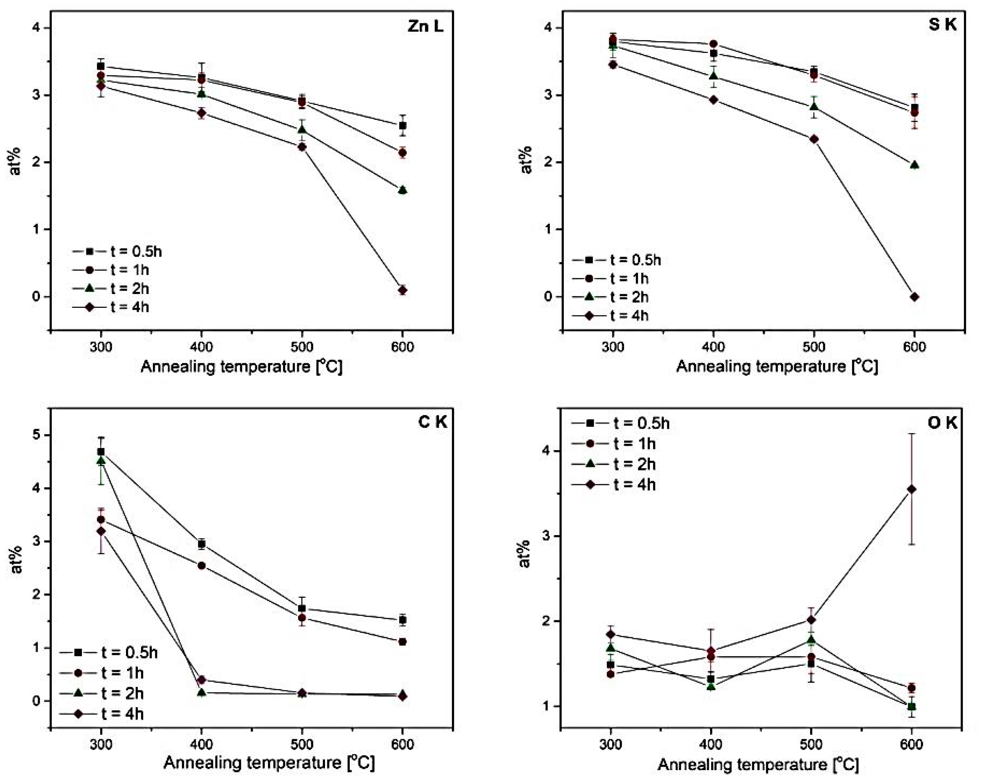
| Temp | Zn L | S K | ||||||||
|---|---|---|---|---|---|---|---|---|---|---|
| As Obtained | 0.5 h | 1 h | 2 h | 4 h | As Obtained | 0.5 h | 1 h | 2 h | 4 h | |
| − | 3.65 ± 0.04 | 8.75 ± 0.23 | ||||||||
| 300 °C | − | 3.42 ± 0.11 | 3.29 ± 0.14 | 3.22 ± 0.06 | 3.14 ± 0.15 | − | 3.80 ± 0.12 | 3.83 ± 0.06 | 3.74 ± 0.18 | 3.45 ± 0.05 |
| 400 °C | 3.26 ± 0.22 | 3.22 ± 0.11 | 3.01 ± 0.04 | 2.73 ± 0.08 | 3.62 ± 0.12 | 3.76 ± 0.02 | 3.27 ± 0.16 | 2.93 ± 0.01 | ||
| 500 °C | 2.91 ± 0.01 | 2.89 ± 0.09 | 2.48 ± 0.15 | 2.23 ± 0.05 | 3.35 ± 0.08 | 3.30 ± 0.01 | 2.82 ± 0.16 | 2.35 ± 0.04 | ||
| 600 °C | 2.55 ± 0.15 | 2.14 ± 0.08 | 1.58 ± 0.05 | 0.10 ± 0.07 | 2.81 ± 0.20 | 2.74 ± 0.23 | 1.96 ± 0.02 | 0.00 ± 0.00 | ||
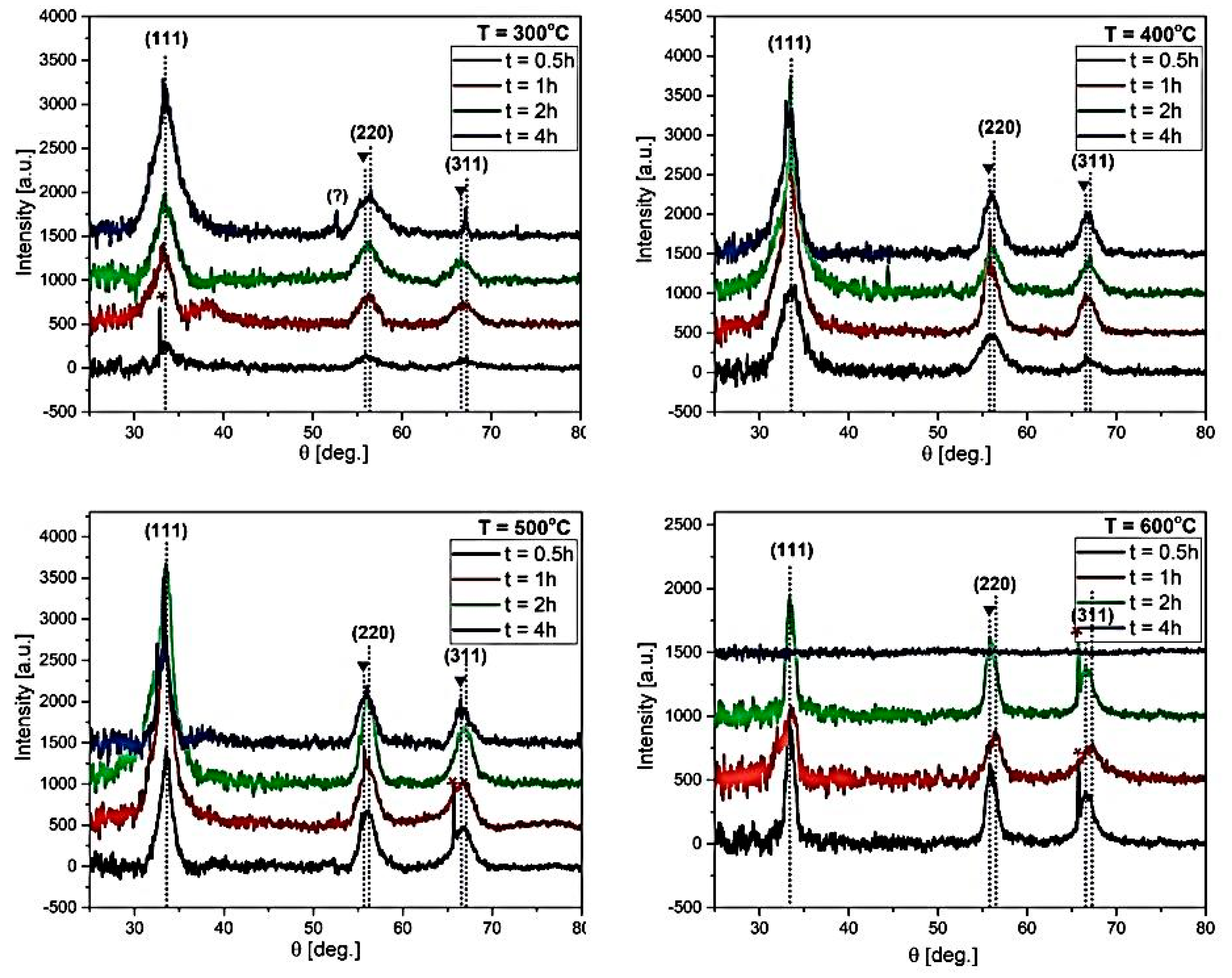
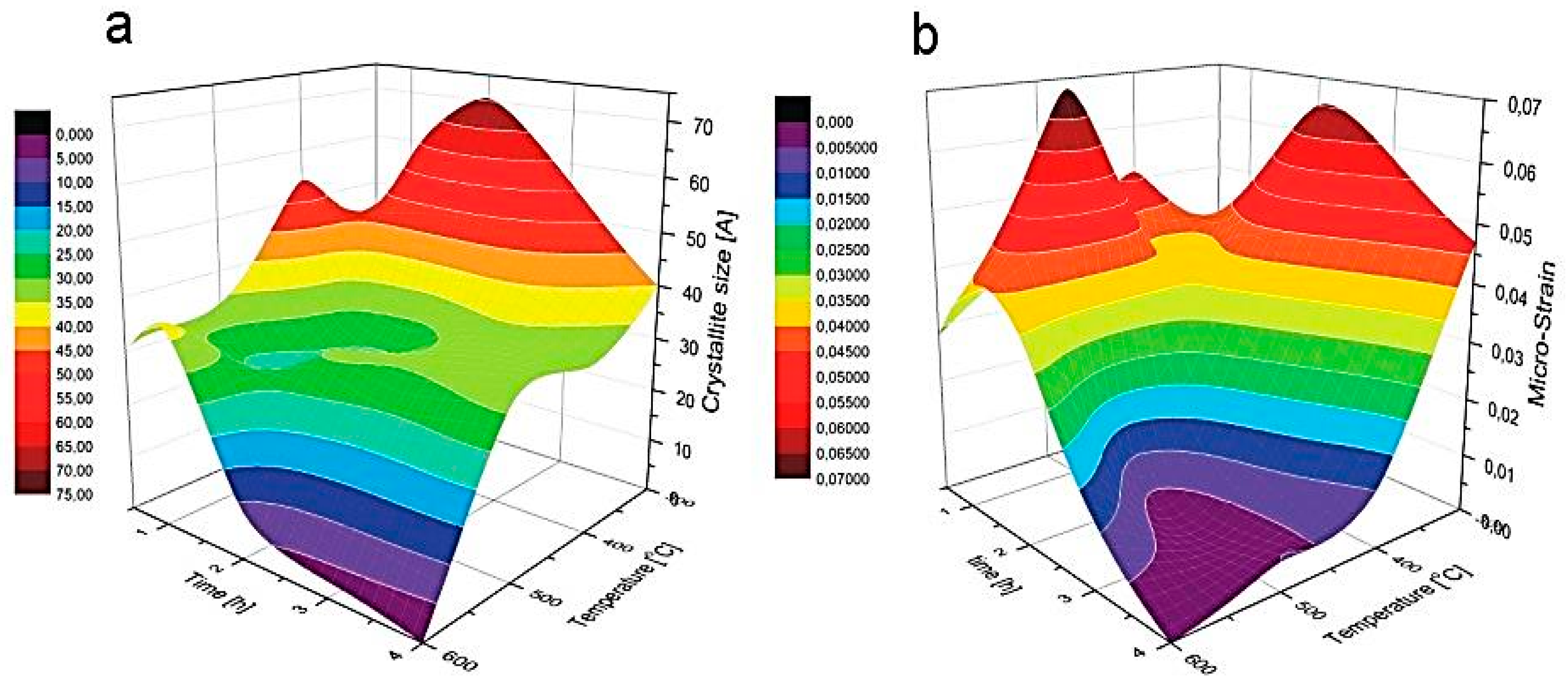
| 0.5 h | Peak Position (Broadening) [2θ] | Crystallite Size D [Å] | Micro-Strain e × 103 | ||
| (111) | (220) | (311) | |||
| 300 °C | 33.07 (2.10) | 55.84 (1.40) | 67.05 (2.50) | 37.42 | 38.97 |
| 400 °C | 33.71 (3.00) | 56.31 (02.44) | 66.56 (1.00) | 53.85 | 51.42 |
| 500 °C | 33.65 (1.89) | 55.98 (2.02) | 66.69 (1.20) | 33.73 | 36.14 |
| 600 °C | 33.36 (1.76) | 56.08 (1.90) | 66.92 (1.62) | 30.65 | 28.28 |
| 1 h | Peak position (broadening) [2θ] | Crystallite size D [Å] | Micro-Strain e × 103 | ||
| (111) | (220) | (311) | |||
| 300 °C | 33.50 (3.19) | 56.31 (2.54) | 66.84 (3.50) | 56.61 | 47.50 |
| 400 °C | 33.18 (1.99) | 55.37 (1.80) | 66.59 (2.01) | 35.07 | 36.32 |
| 500 °C | 33.28 (1.69) | 56.00 (2.07) | 66.97 (3.02) | 23.93 | 69.42 |
| 600 °C | 33.94 (2.10) | 56.57 (1.89) | 67.30 (2.08) | 37.09 | 37.91 |
| 2 h | Peak position (broadening) [2θ] | Crystallite size D [Å] | Micro-Strain e × 103 | ||
| (111) | (220) | (311) | |||
| 300 °C | 33.40 (3.85) | 56.19 (2.00) | 66.61 (2.80) | 70.52 | 65.10 |
| 400 °C | 33.45 (1.75) | 56.11 (2.12) | 66.75 (2.20) | 27.69 | 36.32 |
| 500 °C | 33.51 (1.83) | 56.04 (1.79) | 67.02 (2.28) | 30.81 | 12.50 |
| 600 °C | 33.30 (0.60) | 55.76 (0.69) | 66.50 (1.00) | 08.93 | 33.91 |
| 4 h | Peak position (broadening) [2θ] | Crystallite size D [Å] | Micro-Strain e × 103 | ||
| (111) | (220) | (311) | |||
| 300 °C | 33.27 (2.21) | 55.84 (1,80) | 67.05 (1.43) | 40.04 | 46.90 |
| 400 °C | 33.12 (1.83) | 55.89 (2.06) | 66.62 (1.97) | 30.87 | 10.61 |
| 500 °C | 33.35 (1.90) | 55.82 (2.02) | 66.41 (2.23) | 31.71 | 05.00 |
| 600 °C | − | − | − | − | − |
| Temp | As Obtained | 0.5 h | 1 h | 2 h | 4 h |
|---|---|---|---|---|---|
| − | 2.16 | − | − | − | − |
| 300 °C | − | 1.56 | 4.77 | 2.59 | 4.30 |
| 400 °C | 2.82 | 3.90 | 2.58 | 3.54 | |
| 500 °C | 2.32 | 3.54 | 2.28 | 2.12 | |
| 600 °C | 1.47 | 3.79 | 2.44 | 3.74 |
© 2019 by the authors. Licensee MDPI, Basel, Switzerland. This article is an open access article distributed under the terms and conditions of the Creative Commons Attribution (CC BY) license (http://creativecommons.org/licenses/by/4.0/).
Share and Cite
Włodarski, M.; Chodorow, U.; Jóźwiak, S.; Putkonen, M.; Durejko, T.; Sajavaara, T.; Norek, M. Structural and Optical Characterization of ZnS Ultrathin Films Prepared by Low-Temperature ALD from Diethylzinc and 1.5-Pentanedithiol after Various Annealing Treatments. Materials 2019, 12, 3212. https://doi.org/10.3390/ma12193212
Włodarski M, Chodorow U, Jóźwiak S, Putkonen M, Durejko T, Sajavaara T, Norek M. Structural and Optical Characterization of ZnS Ultrathin Films Prepared by Low-Temperature ALD from Diethylzinc and 1.5-Pentanedithiol after Various Annealing Treatments. Materials. 2019; 12(19):3212. https://doi.org/10.3390/ma12193212
Chicago/Turabian StyleWłodarski, Maksymilian, Urszula Chodorow, Stanisław Jóźwiak, Matti Putkonen, Tomasz Durejko, Timo Sajavaara, and Małgorzata Norek. 2019. "Structural and Optical Characterization of ZnS Ultrathin Films Prepared by Low-Temperature ALD from Diethylzinc and 1.5-Pentanedithiol after Various Annealing Treatments" Materials 12, no. 19: 3212. https://doi.org/10.3390/ma12193212
APA StyleWłodarski, M., Chodorow, U., Jóźwiak, S., Putkonen, M., Durejko, T., Sajavaara, T., & Norek, M. (2019). Structural and Optical Characterization of ZnS Ultrathin Films Prepared by Low-Temperature ALD from Diethylzinc and 1.5-Pentanedithiol after Various Annealing Treatments. Materials, 12(19), 3212. https://doi.org/10.3390/ma12193212