3.1. Growth Mechanism of the HEF
The HEF (sample #1) was prepared by magnetron co-sputtering deposition system with an alloy target and a pure Al target.
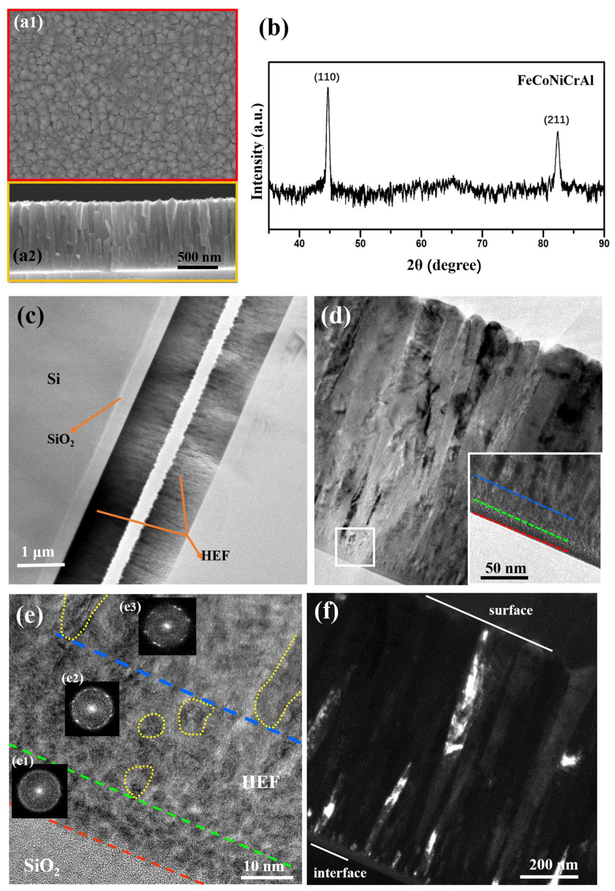
Figure 1 shows the results of the microstructure and phase of the sample. The SEM images of film surface and internal cross-section are shown in
Figure 1(a1,a2), indicating that the sample consists of irregularly-shaped columnar grains. The in-plane grains have polygon morphology and the statistical grain size is 92 ± 26 nm. The columnar crystal structure is confirmed by the cross-sectional image and the top of the columnar grains has angle shape. The thickness of the film is 978 ± 5 nm.
Figure 1b shows the XRD pattern of the HEF. Grazing incidence mode was used in the XRD measurement to avoid the interference of the substrate signal. The diffraction peaks located at 44.6° and 82.3° indicate that the FeCoNiCrAl phase with bcc structure is formed.
A cross-sectional TEM image of the HEF (
Figure 1c) shows that the film was deposited on the SiO
2/Si substrate and the thickness of the SiO
2 is about 300 nm.
Figure 1d is the enlarged image of the film and the thickness of the film measured from TEM image is 980 ± 4 nm, which is consistent with the result of SEM image. Most of the grains exhibit a columnar structure in the sample and the width of a columnar grain is related to the location. The portion of columnar grain close to the surface is wider than that close to the substrate, hence the shape of the columnar grain is like a ladder from the cross-sectional view. Besides, the partial area which is very close to the substrate has a special microstructure. The top-right inset is the enlarged image of the selected area (white box) in
Figure 1d and clearly shows the difference from columnar crystal structure. Amorphous structure (located between red line and green line) and equiaxial nanocrystalline structure (located between green line and blue line) exist in this area, and columnar crystal forms above the nanocrystalline region. The width of the amorphous region and nanocrystalline region is approximately 8 nm and 20 nm respectively.
Figure 1e is the high-resolution TEM (HRTEM) image of the region very close to the substrate, and the insets (
Figure 1(e1–e3)) are the fast Fourier transform (FFT) patterns of the corresponding area. Some domains with sizes of about 2 nm exist in the region next to the substrate and the atomic arrangement is disordered in the domains. The FFT shows the amorphous holes without diffraction points, which demonstrate the amorphous structure in this region. Above the amorphous region, some equiaxial nanograins (labeled as a yellow dotted line between a green dotted line and a blue dotted line) are observed and the FFT pattern with a polycrystalline ring also confirmed the nanocrystalline structure.
Figure 1(e3) is the FFT pattern of the area above the nanocrystalline region, which shows the diffraction points clearly. The grain shape tends to be columnar and the grain size becomes larger (labeled by a yellow dotted line above the blue dotted line). The closer to the film surface, the larger the columnar crystal grain size.
Figure 1f is dark-field TEM image of the film, and the bright areas represent grains with the same orientation. A region with gray contrast existing above the interface, between substrate and HEF, indicates the amorphous structure. Additionally, a lot of bright areas with small sizes represent the equiaxial nanograins. Above the nanocrystalline region, some large bright areas indicate the existence of columnar grains. The regions containing amorphous domains and nanocrystalline structure were also observed in other samples which are not shown here.
During the film deposition process, the atoms on the target surface were sputtered by high-energy argon ions and then were deposited onto the substrate under the effect of a dual function of magnetic and electric fields. The process of coating atoms depositing onto the substrate to form the thin film occurs in three steps: nucleation, islands growth and coalescence, and grain coarsening [
21,
22]. For the HEF, the sputtered atoms with energy interact with the surface atoms of substrate, and become loosely-bonded adatoms by transferring kinetic energy. The island structure forms by the adatoms’ aggregation and diffusion. As the number of sputtered atoms increases, the island coalesces to be a small domain under the driving force of atomic diffusion. The adatoms are composed of five kinds of atoms with different atomic radii, leading to the difficulty to form ordered crystal islands in the initial stage. Hence, the structure of the region near the substrate is amorphous.
After the amorphous domain formation, the sputtered atoms would exchange energy with the high entropy domain rather than substrate atoms. The domains support some sites with low energy to make the sputtered atoms grow extendedly, and then the nanograins with small grain size form. As the continued deposition of energetic atoms, film thickening proceeds through local epitaxy on the individual grains to form columnar grains, accompanying the recrystallization and atoms’ surface migration. In the whole process, the energy of sputtered atoms and the energy of deposited atoms on the substrates are the key factors affecting the film formation.
3.2. The Effects of Deposition Parameters on Microstructure and Elemental Uniformity
The power loaded on the target and the substrate temperature determine the energy of sputtered atoms and deposited atoms, respectively. Besides, the crystal orientation of substrate would affect the island formation during the film deposition. Therefore, the power, substrate temperature and the type of substrate are three important parameters that could affect the phase and microstructure of HEF. FeCoNiCrAl HEFs with different deposition conditions were prepared (summarized in the
Table 1) to investigate the effects of the parameters.
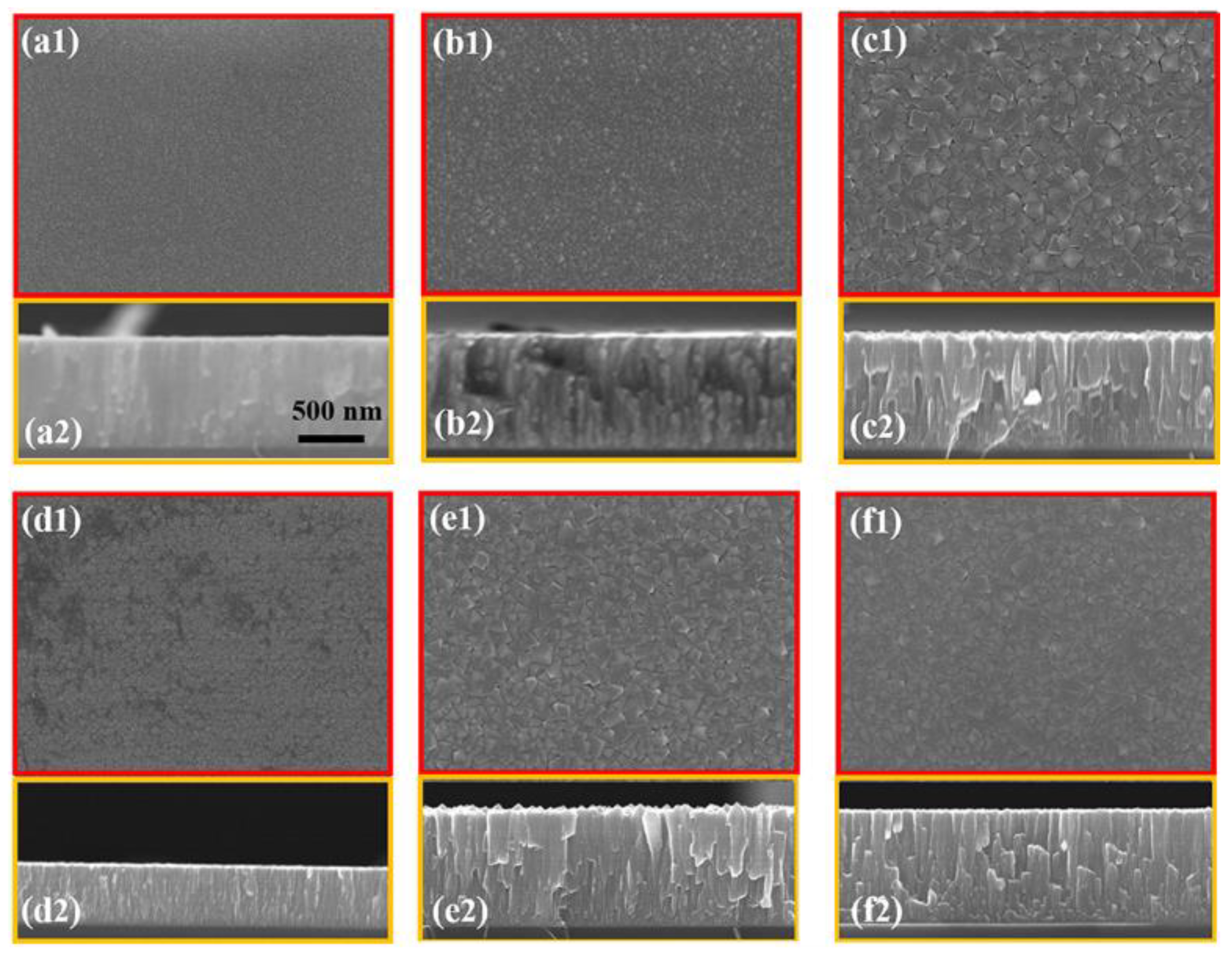
Figure 2 is the SEM images of HEF samples with different deposition parameters, including plan-view images (
Figure 2(a1–f1)) and corresponding cross-sectional images (
Figure 2(a2–f2)). All of the images have the same scale bar, as marked in
Figure 2(a2).
Figure 2a–c represent the images of the HEF samples deposited on substrate of Si (100) with the power of 300 W. The substrate temperatures (T) are room temperature (RT), 250 °C and 350 °C respectively. The surface of these samples is intact without holes or cracks, and the thickness of the films is about 975 ± 5 nm.
The edge profile of the grain is smooth when the substrate temperature is RT, as shown in
Figure 2(a1). By counting the grain size from the plan-view SEM image, the statistical grain size of the columnar crystals close to the surface is 14 ± 3 nm. The characteristic of columnar crystal is not obvious from the cross-sectional view (
Figure 2(a2)). When T = 250 °C, the sample grain size increases to 38 ± 10 nm (
Figure 2(b1)), and the anisotropic grains composed of small crystal grains are observed, as shown in
Figure 2(b2). When T = 350 °C,
Figure 2(c1) exhibits the irregularly-shaped grains with an average size of 91 ± 28 nm, and the obvious columnar crystal structure occurs (
Figure 2(c2)). This indicates that as the substrate temperature increases, the grain shape changes from round to polygon with the increase of the grain size.
Figure 2d illustrates the HEF sample deposited on Si (100) with the substrate temperature of 350 °C, and the power reduced to 100 W. Compared with sample #4 deposited with power of 300 W (as shown in
Figure 2c), the statistic grain size of this sample decreases to 25 ± 6 nm and the edge profile of the crystal is more rounded (
Figure 2(d1)). This means the power is a significant factor affecting the grain size of columnar crystal. The characteristic columnar crystals are observed in
Figure 2(d2). The film with the thickness of 247 ± 4 nm is thinner than other films due to the lower deposition rate.
Figure 2e,f show the SEM images of the samples, which were deposited on substrates of Si (110) and SiO
2/Si, respectively, and the power was 300 W with T = 350 °C. These two samples had little difference in their morphologies with the sample #4 which was deposited on substrate of Si (100) with a power of 300 W and substrate temperature of 350 °C. The statistical grain sizes are 89 ± 26 nm and 86 ± 23 nm, respectively, which are also close to the grain size of the sample #4. The results suggest that the structure of HEFs is almost unaffected by the crystal orientation of substrate.
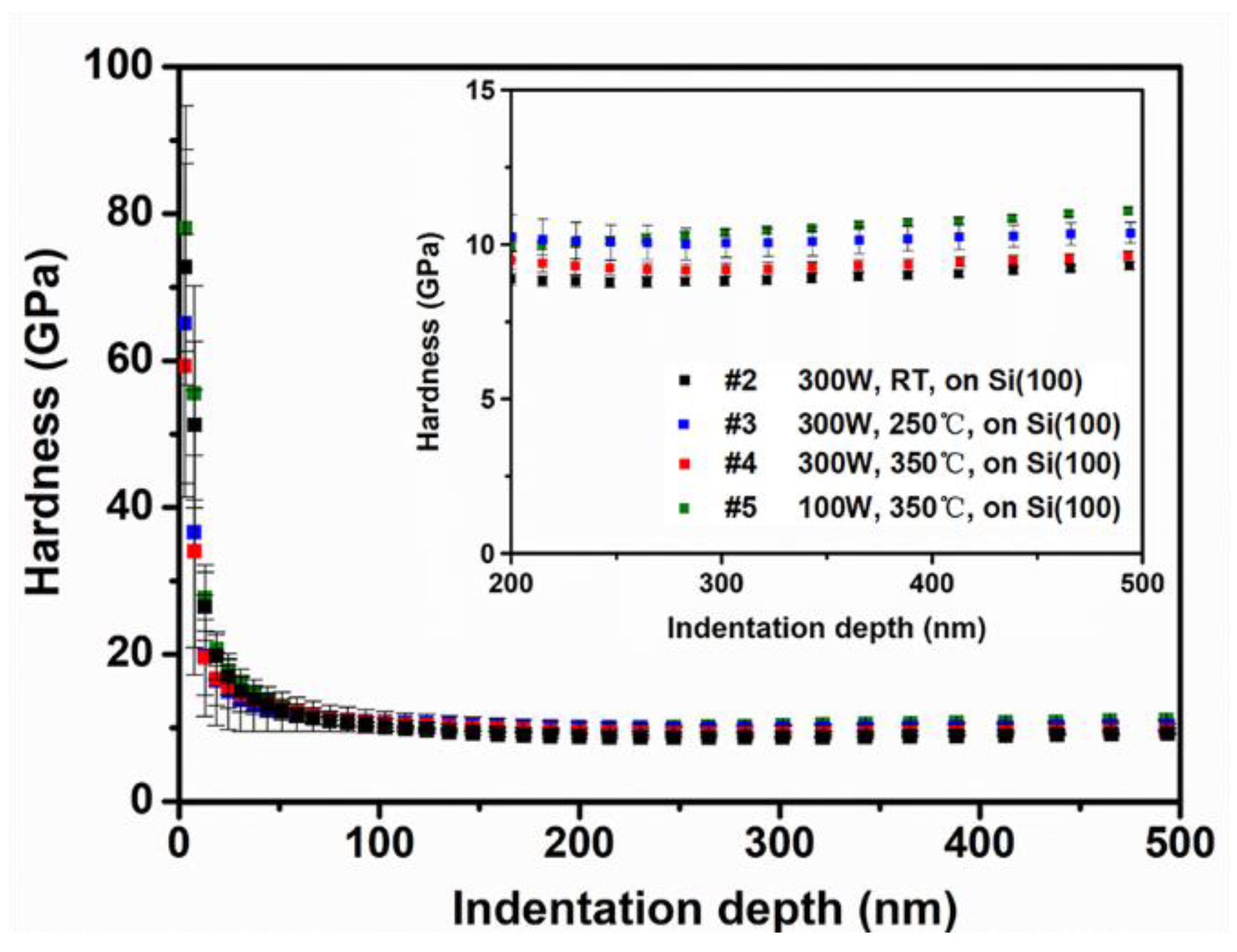
The substrate temperature and the power significantly affect the morphology and grain size of HEF. A microstructure at the atomic scale is necessary to explore.
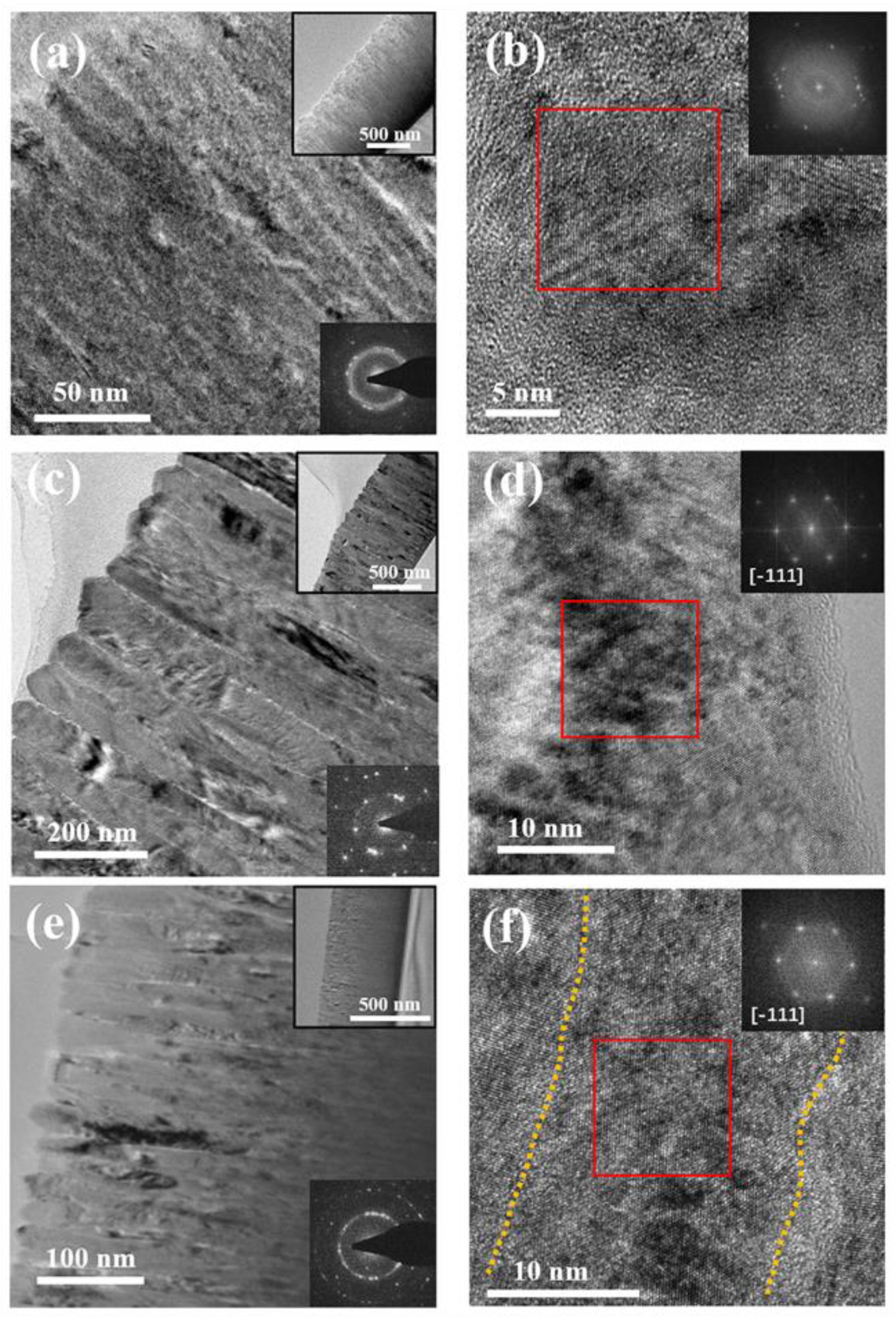
Figure 3 illustrates the detailed microstructure of HEF samples #2, #4 and #5, which were all deposited on the substrate of Si (100).
Figure 3a represents the TEM image of HEF with the substrate temperature of RT and the power of 300 W. The top-right inset is the low-magnification image to demonstrate the overall condition of the film. The grain boundary of the sample cannot be clearly observed. The bottom-right inset is the selected area electron diffraction (SAED) pattern of the sample. It exhibits amorphous holes, except for diffraction points, indicating that crystal structures together with amorphous structures exist in the film. The HRTEM image shown in
Figure 3b demonstrates the nanocrystal with small grain size and the disordered structure in some areas. The corresponding FFT pattern (top-right inset in
Figure 3b) shows multiple crystal orientations, indicating the polycrystalline structure. All of the results confirm that the crystallinity of the HEF sample deposited at room temperature is not good enough. What happens under a higher substrate temperature?
Figure 3c,d clearly shows the microstructure of HEF samples deposited at the substrate temperature of 350 °C. The depth of the columnar crystal is clearly observed in
Figure 3c and the average width of columnar grain is about 82 nm. The high aspect-radio of the columnar grains results from the anisotropy growth velocity under deposition [
23]. The edge profile of the columnar grain near the surface is choppy, resulting from the wide angular distribution of the deposition flux and atomic shadowing [
21]. The SAED pattern (bottom-right inset in
Figure 3c) shows the diffraction points without amorphous holes, implying that the sample has a relatively complete crystal structure.
Figure 3d is an HRTEM image of one columnar grain in
Figure 3c, illustrating the ordered lattice arrangement. The FFT pattern (top-right inset in
Figure 3d) of the red box area indicates that crystal orientation of this grain is [−111]. Combining with the measured lattice spacing (0.208 nm), it can be clarified that FeCoNiCrAl phase with bcc structure is formed in the film.
Figure 3e,f show the TEM images of HEF sample deposited at a substrate temperature of 350 °C with a power of 100 W. The columnar crystal structure could also be observed and the average width of the columnar grain is about 22 nm, which is smaller than that of the sample deposited using a power of 300 W. Besides, most columnar grains are closely arranged together and no distinct gaps or intra-columnar voids exist. The polycrystalline ring illustrated in the SAED pattern (bottom-right inset in
Figure 3e) indicates that the polycrystalline structure with a small grain size has more complicated crystal orientations. Detailed crystal structure is characterized by HRTEM (
Figure 3f), which is similar to the sample deposited with power of 300 W. FFT pattern (top-right inset in
Figure 3f) of the red box area indicates that the crystal orientation is [−111] and the columnar grain has a perfect single crystal structure. Meanwhile, the grain boundaries between columnar grains are clearly observed, marked by the dotted line. The edge profile of the columnar grain is more smooth than that of sample #4. These results clarify that HEF sample deposited using a power of 100 W with the substrate temperature of 350 °C has a good-crystallinity structure with small grain size.
The microstructure of the HEF deposited at room temperature is a nanocrystalline structure with some disordered structure, and no distinct columnar crystal structure is observed. In contrast, all of the films deposited at higher substrate temperature have a good crystallinity without amorphous structure. During the deposition of films, the energy of deposited adatoms affects the ability and rate of migration, which would be determined by the substrate temperature. The sputtered atoms interact with the atoms on the substrate at room temperature and become the adatoms by exchanging energy. Then, some adatoms are captured at low-energy lattice sites to form nanocrystals [
22]. When the low-energy lattice sites are filled up, the remaining adatoms do not have enough energy to migrate to the stable lattice sites, and the disordered structure forms by these adatoms. The higher substrate temperature provides energy for the deposited adatoms to support their migration to form a continuous crystal structure. As a result, the crystal quality could be improved by increasing the substrate temperature.
After the crystal structure forms in the HEF, the growth of the grain is controlled by two processes: adatom surface diffusion and recrystallization through grain boundary migration. The power of the target provides energy for sputtered atoms to interact with atoms on the substrate. The energy of sputtered atom is obtained from the energy exchange with positive ions, which is dependent on the electric field and magnetic field controlled by power. Higher power would increase the kinetic energy and the flux of sputtered atoms, which makes the surface diffusion of adatoms easier [
21], resulting in the growth of grain size. The recrystallization through grain boundary migration is affected by the substrate temperature. The grain size increases with increasing substrate temperature because of the enhanced thermal migration of grain boundary under deposition [
24,
25]. Hence, reducing the substrate temperature and power provides the opportunity to decrease the grain size. Nevertheless, the lower substrate temperature could cause the poor crystallinity. Therefore, the deposition condition of higher substrate temperature and lower power can be used to prepare HEF samples with small grain size and high crystalline quality. In general, the crystal orientation of the substrate would affect the crystallinity of the film by generating stress when the island forms. However, the structure formed in the initial stage is an amorphous domain in the HEF sample, which is less affected by the stress. As a result, the microstructure of HEFs is almost unaffected by the crystal orientation of the substrate.
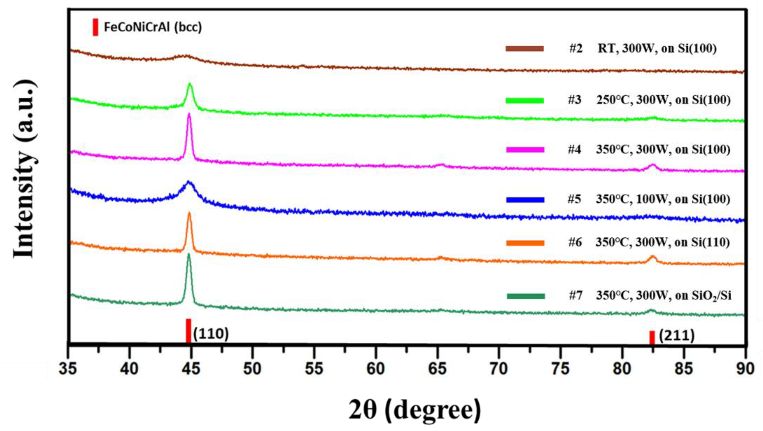
To further reveal the effect of the key parameters on phase composition of HEF, XRD experiments were conducted in grazing incidence mode.
Figure 4 illustrates the XRD patterns of the HEF samples prepared with different parameters. All of the spectrums emerge an easy-to-observe peak, which has the position of 44.6°, indicating the formation of bcc-structured FeCoNiCrAl phase with (110) plane in the film. Besides, samples #3, #4, #6 and #7 also have a small peak at the position of 82.3° representing the bcc-structure FeCoNiCrAl phase with a (211) plane. The XRD results illustrate that all the film samples have a preferred orientation of [110] with single bcc structure, which is different from the FeCoNiCrAl high entropy alloys prepared by other methods having mixed phase structures [
26,
27]. To further examine the average grain size of axial columnar crystal, the full width at half maximum (FWHM) of the main peak is given in
Table 2, and the average grain size is calculated using Scherrer formula
where the Scherrer constant K = 0.89, wavelength λ = 0.154 nm and B = FWHM. The results of samples #2, #3 and #4 illustrate that high substrate temperature would promote the growth of crystal size. Besides, the low power results in smaller grain size of the columnar crystal by comparing the results of samples #4 and #5. Meanwhile, the type of substrate has no significant effect when analyzing the results of samples #4, #6 and #7, which is consistent with previous results.
To characterize the chemical composition of the HEF samples, EDS measurements were carried out to explore the atomic ratio and distribution of the elements.
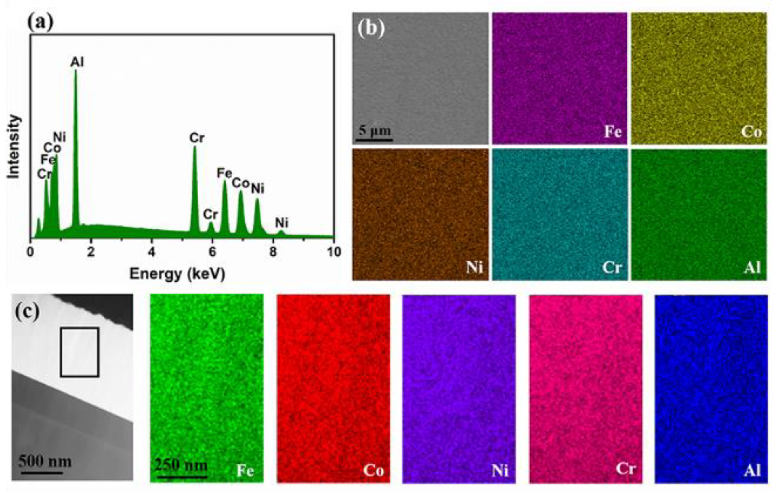
Figure 5 shows the SEM-EDS results and STEM-EDS results of HEF sample #1, illustrating the elemental distribution from plan-view and cross-sectional view, respectively. The spectroscopy (
Figure 5a) indicates that the film consists of five elements (Fe, Co, Ni, Cr and Al) in a near-equal atomic percentage (19.4:19.5:20.5:20.0:20.6) without obvious difference between the solute and solvent. The elemental distribution in plan-view was characterized by SEM-EDS (
Figure 5b) and the results show that the five elements are uniformly distributed without segregation. The EDS mapping with higher magnification was conducted, and the result is consistent.
Figure 5c shows the STEM image of the film from a cross-sectional view and the EDS mapping of the selected area, confirming that the HEF sample has a random distribution of the five elements in the cross-sectional view. The similar results are observed in other HEF samples (not shown here). The chemical composition uniformity of the sample prepared by magnetron sputtering is better than other techniques, such as art melting and hot compression [
27,
28,
29], benefiting from the process of sputtering and deposition at the atomic scale [
30].
EDS is a common method that could be used to characterize the chemical composition of materials [
29,
31]. Nevertheless, the depth that EDS detects reaches hundreds of nanometers. This means the results of EDS represent an average over the range of the certain depth. In order to investigate the elemental uniformity of the sample surface clearly, a novel method was introduced to the characterization of HEFs. Scattering-type scanning near-field optical microscopy (s-SNOM) has resolved the optical diffraction limit and exhibits the ability of imaging with nano-scale resolution [
32]. Usually, it is built as a bimodal tool comprising both s-SNOM and AFM. In a common setting, the tip of a metal-coated AFM probe is illuminated by a laser beam during the sample-scanning and the scattered light from the tip-sample interaction volume is detected using an interferometric detection scheme for suppressing the background light. The setting permits the acquisition of both AFM and s-SNOM images simultaneously. The most preferred interferometric detection scheme is known as “pseudo-heterodyne” [
33] using a modified Michelson interferometer, allowing for simultaneous acquisition of both amplitude and phase images of the scattered light.
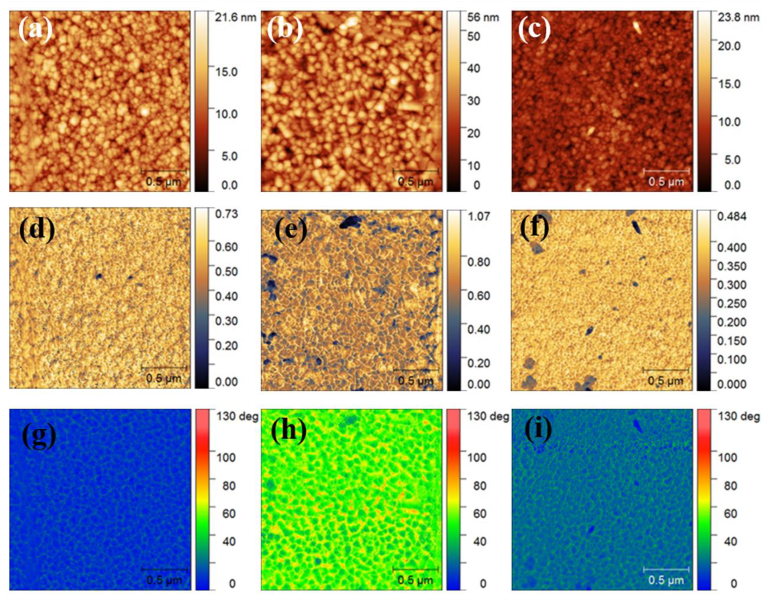
Figure 6 shows the AFM images (
Figure 6a–c), s-SNOM amplitude images (
Figure 6d–f) and phase images (
Figure 6g–i) of the HEF samples #2, #4 and #5, respectively. While the AFM images reveal the topography of the sample surface, the s-SNOM images (amplitude and phase) reveal the optical properties of the samples. According to the general conception, the amplitude signal is linked to the dispersion, while the phase signal is linked to the optical absorption [
34,
35]. The surfaces of HEF samples deposited at room temperature with the power of 300 W (sample #2) and at 350 °C with the power of 100 W (sample #5) have similar morphologies, which consist of round particles of small sizes (
Figure 6a,c). In contrast, polygonal-shaped features appear on the surface of HEF sample deposited at 350 °C with the power of 300 W (sample #4), as shown in
Figure 6b. The HEF sample #4 has the roughest surface because of the large grain size. Samples #2 and #5 have similar amplitudes and phase images (
Figure 6d–g,i), indicating the dispersion and absorption properties of the HEF samples are similar. Meanwhile, the amplitude and phase SNOM images of samples #4 are obviously different, shown in
Figure 6e,h. In general, the chemical composition and the surface topography could affect the optical properties of the sample, hence resulting in SNOM images. The larger grain size and surface roughness of sample #4 results in the obvious difference in its SNOM images compared with the images of other two samples.
In order to explain the results quantitatively, the entropy calculation which reflects the uniformity of chemical composition was conducted by using the s-SNOM data. The Shannon information entropy and the gray-level co-occurrence (GLCM) entropy were calculated. The Shannon information entropy and GLCM entropy are used to investigate the uniformity of element distribution. Set the discrete variate
X having
n possible values (
x1,
x2, …,
xn) and each value of probability is [
p(
x1),
p(
x2), …,
p(
xn)]. The Shannon information entropy of X is defined as follows:
In the case of an image, the discrete variates X are the pixel values, while p(xi) is the probability of occurrence of a pixel value xi. The calculated Shannon information entropies are 6.78 ± 0.28, 7.27 ± 0.22 and 6.91 ± 0.15 for samples #2, #4 and #5, respectively. The GLCM matrix is a second-order statistical method which provides information on the spatial relationships between intensities of the pixels in a given image. The entropy is calculated with the GLCM texture plugin in the software of ImageJ. The GLCM is constructed by counting the number of occurrences of a gray level adjacent to another gray level, at a specified pixel distance. Each result is divided by the total number of elements to obtain a probability. The matrix elements are the probability of the gray level co-occurrence between pixels, with the rows and columns of the matrix representing the gray levels in the image. The matrix can be computed for adjacent pixel either in horizontal (0°), vertical (90°) or diagonal (45°, 135°) direction. In our case, average values for the four directions were considered for the computed parameters. Thus, we proposed to calculate the entropy more precisely by examining the mentioned organization parameters.
The calculated results inform that the GLCM entropy of the sample #4 was the largest, which was 8.70 ± 0.22. The samples #2 and #5 had GLCM entropies of 8.51 ± 0.24 and 8.60 ± 0.22, respectively. Higher entropy suggests a higher disorder, indicating the better uniformity of element distribution. Combining the results of Shannon entropy, we can conclude that the chemical composition distribution of the HEF deposited at 350 °C using a power of 300 W is more uniform than that of HEF deposited at room temperature and that of HEF deposited using a power of 100 W. The deposited adatoms get more energy in the substrate with a high temperature, resulting in the faster migration rate in the HEF. On the other hand, the power determines the movement of sputtered atoms, and increasing the power could effectively increase the interaction energy. Therefore, the elemental uniformity can be optimized by using high substrate temperature and power during the film deposition.


 ,
, 


