Synthesis of Vertically Oriented Graphene Sheets or Carbon Nanowalls—Review and Challenges


Abstract
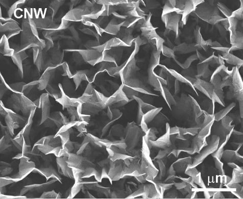
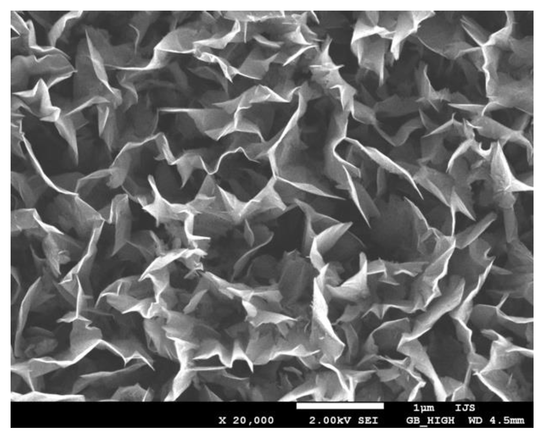
1. Introduction
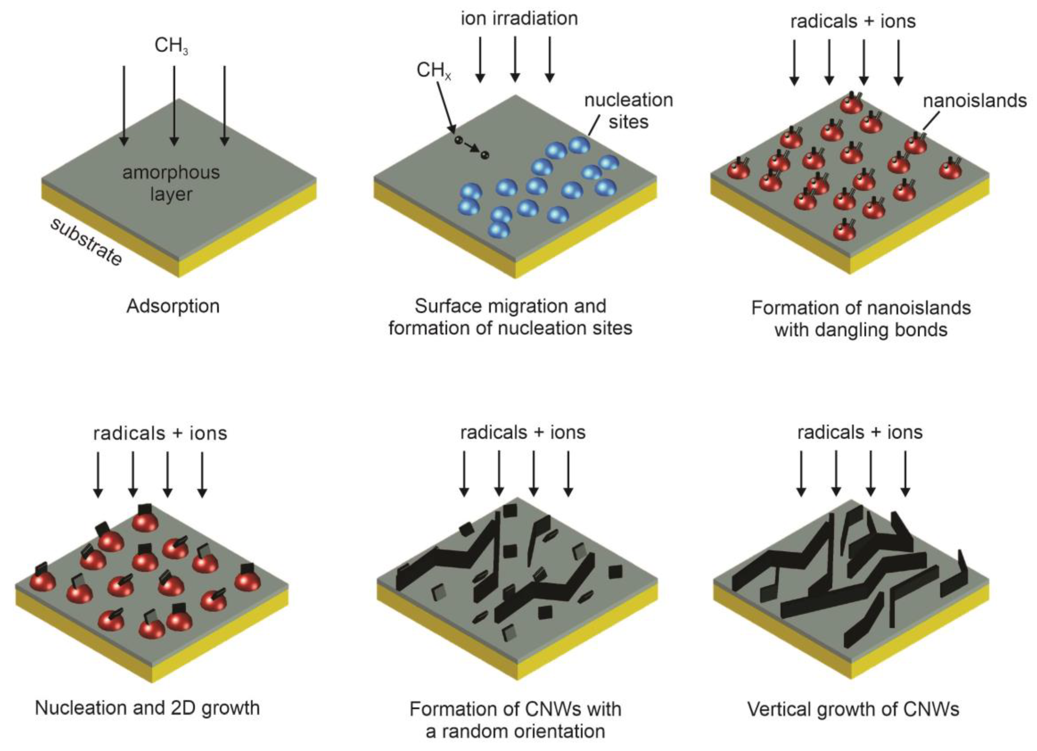
- Adsorption of CH3 radicals and formation of amorphous carbon layer on the substrate.
- Formation of defects and dangling bonds because of ion irradiation leading to the formation of nucleation sites.
- Migration of carbon species and formation of nanoislands with dangling bonds.
- Nucleation of small graphene nanosheets on dangling bonds followed by a two-dimensional growth.
- Formation of nanographene sheets with a random orientation.
- Bonding of reactive carbon species to the edge of graphene sheets. Nanosheets that are standing almost vertically preferably grow faster and shadow low-lying graphene sheets, therefore their growth is suppressed.
2. Early Scientific Documents of Plasma Synthesis of Carbon Nanowalls
3. A Brief Review of Patents
4. Summary of Literature Review on PECVD Deposition of CNWs
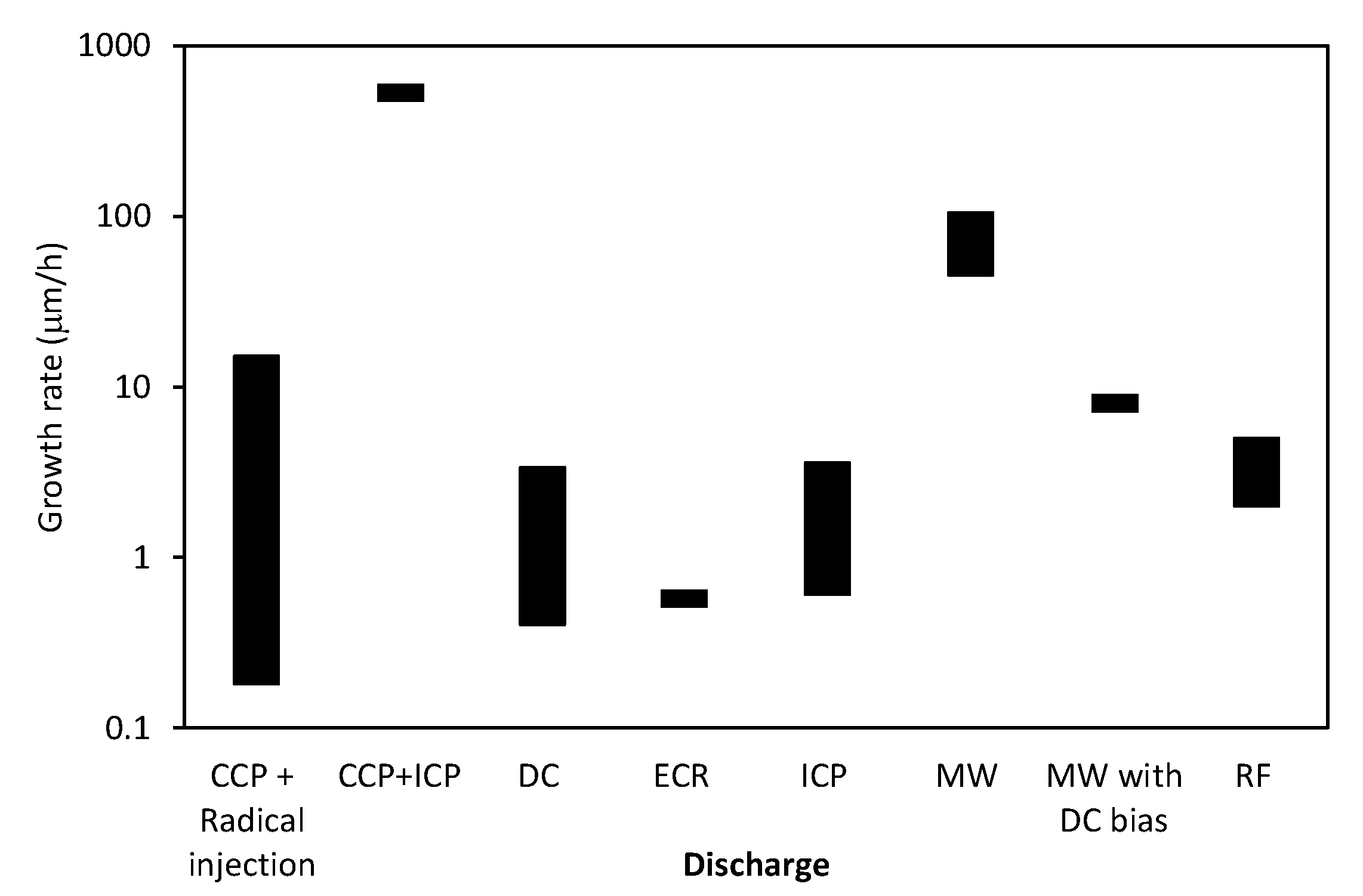
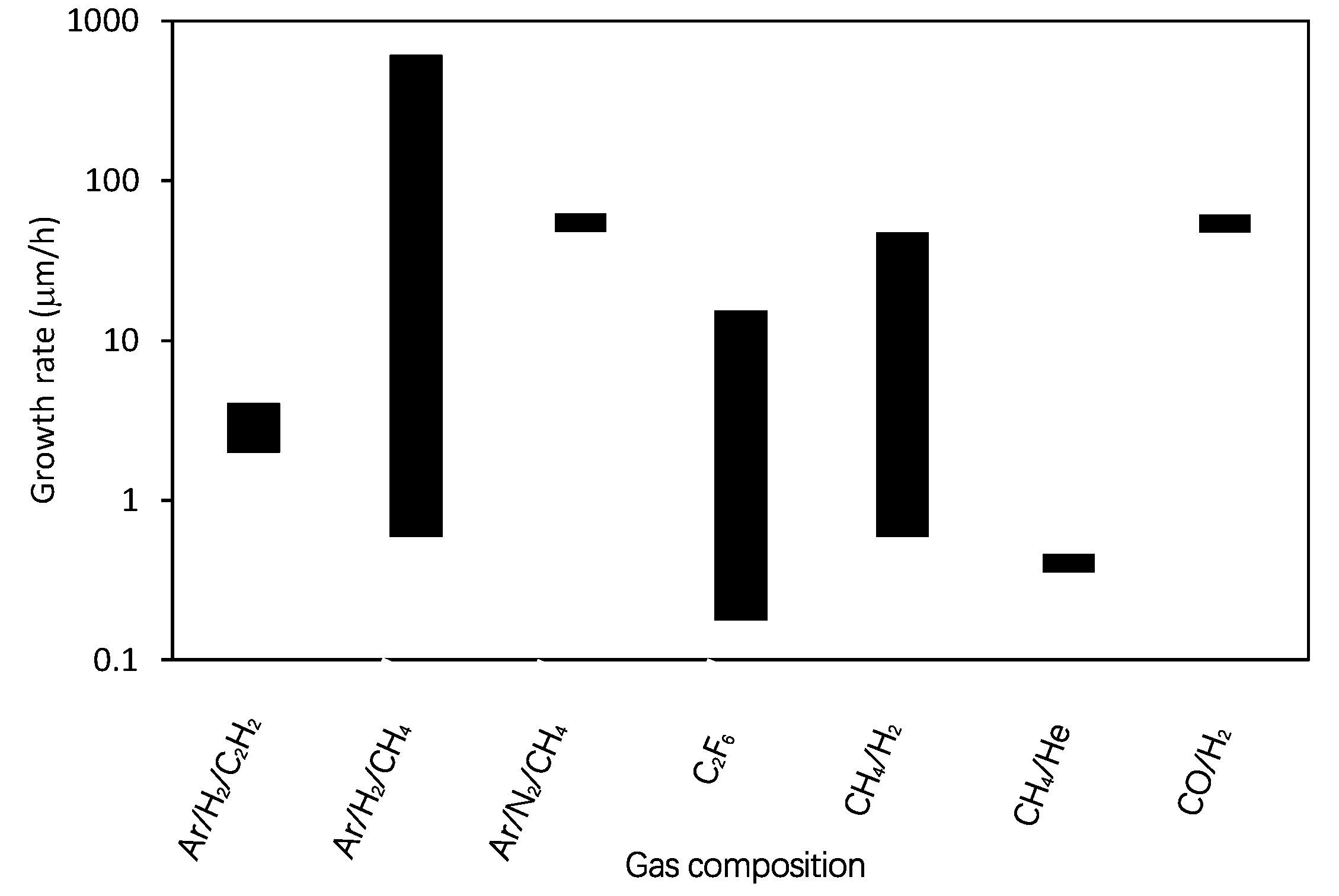
5. Comparison of Available Literature
- Either gaseous plasma or hot wires are used for production of reactive carbon-containing molecules that stick to the surface substrate and cause growing of CNWs on said substrate;
- Reactive carbon containing molecules are usually produced from hydrogenated carbon precursors, sometimes fluorinated, or from carbon oxide
- Precursors are essentially gaseous and are continuously leaked into a reaction chamber to facilitate growing of CNWs. The gases are continuously removed from the reaction chamber;
- Hydrogen is leaked into the reaction chamber simultaneously with hydrogenated carbon precursors in order to obtain good quality nanowalls. Noble gases are often added into the gas mixture leaked into the reaction chamber to alter the quality of CNWs
- Metallic catalysts were applied in early documents but have been omitted later;
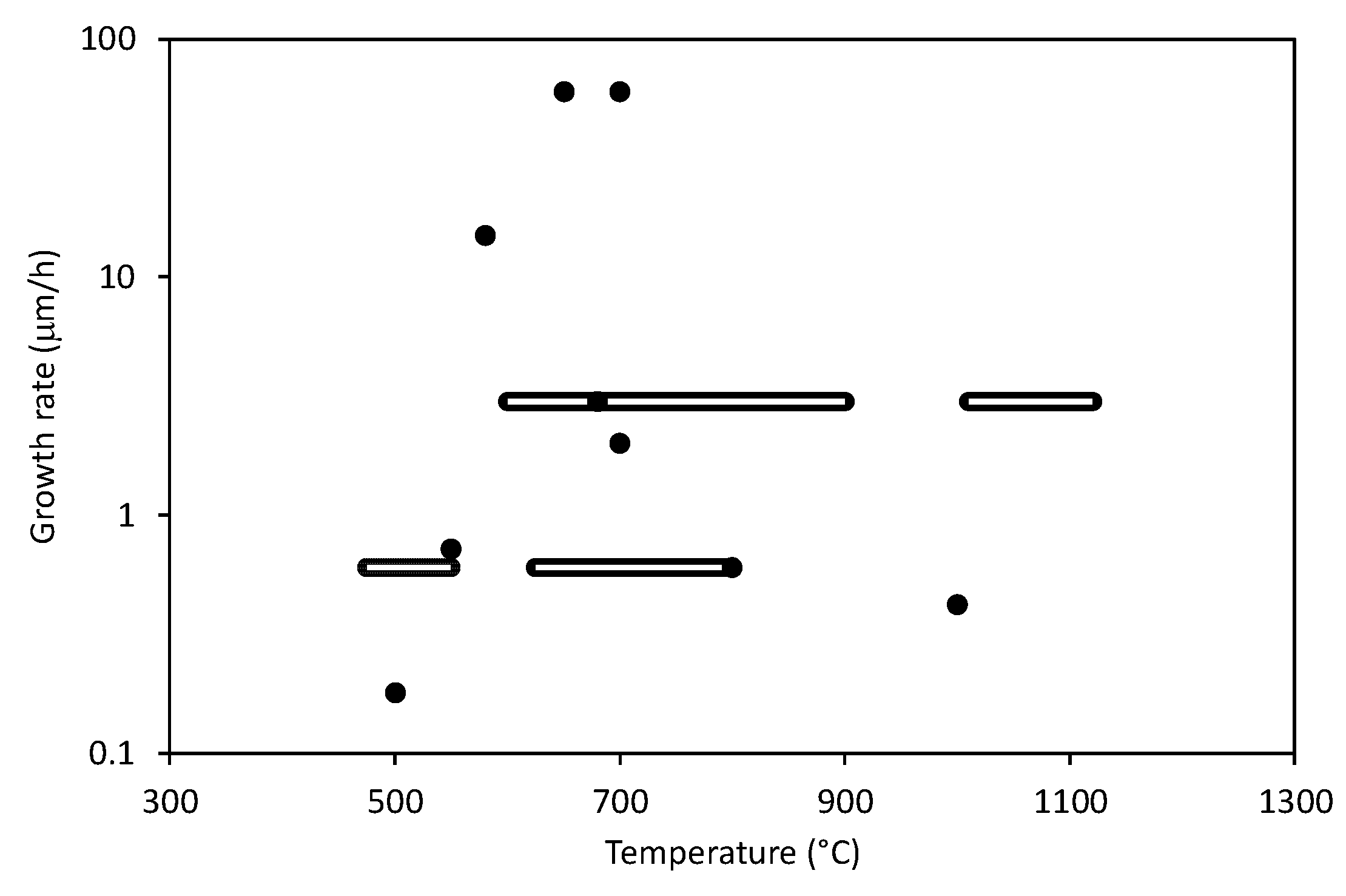
- Elevated temperatures of the substrates (usually in the range of 600–800 °C) are needed for CNWs growth.
6. Challenges and Roadmap
Author Contributions
Funding
Conflicts of Interest
References
- Kwon, S.H.; Kim, H.J.; Choi, W.S.; Kang, H. Development and performance analysis of carbon nanowall-based mass sensor. J. Nanosci. Nanotechnol. 2018, 18, 6552–6554. [Google Scholar] [CrossRef] [PubMed]
- Li, J.H.; Zhu, M.J.; An, Z.L.; Wang, Z.Q.; Toda, M.; Ono, T. Constructing in-chip micro-supercapacitors of 3D graphene nanowall/ruthenium oxides electrode through silicon-based microfabrication technique. J. Power Sources 2018, 401, 204–212. [Google Scholar] [CrossRef]
- Liu, L.L.; Guan, T.; Fang, L.; Wu, F.; Lu, Y.; Luo, H.J.; Song, X.F.; Zhou, M.; Hu, B.S.; Wei, D.P.; et al. Self-supported 3D NiCo-LDH/Gr composite nanosheets array electrode for high-performance supercapacitor. J. Alloy Compd. 2018, 763, 926–934. [Google Scholar] [CrossRef]
- Sarani, A.; Nikiforov, A.Y.; De Geyter, N.; Morent, R.; Leys, C. Surface modification of polypropylene with an atmospheric pressure plasma jet sustained in argon and an argon/water vapour mixture. Appl. Surf. Sci. 2011, 257, 8737–8741. [Google Scholar] [CrossRef]
- Shin, S.C.; Yoshimura, A.; Matsuo, T.; Mori, M.; Tanimura, M.; Ishihara, A.; Ota, K.; Tachibana, M. Carbon nanowalls as platinum support for fuel cells. J. Appl. Phys. 2011, 110, 104308. [Google Scholar] [CrossRef]
- Krivchenko, V.A.; Itkis, D.M.; Evlashin, S.A.; Semenenko, D.A.; Goodilin, E.A.; Rakhimov, A.T.; Stepanov, A.S.; Suetin, N.V.; Pilevsky, A.A.; Voronin, P.V. Carbon nanowalls decorated with silicon for lithium-ion batteries. Carbon 2012, 50, 1438–1442. [Google Scholar] [CrossRef]
- Takeuchi, W.; Kondo, H.; Obayashi, T.; Hiramatsu, M.; Hori, M. Electron field emission enhancement of carbon nanowalls by plasma surface nitridation. Appl. Phys. Lett. 2011, 98, 123107. [Google Scholar] [CrossRef]
- Wei, W.; Hu, Y.H. Highly conductive Na-embedded carbon nanowalls for hole-transport-material-free perovskite solar cells without metal electrodes. J. Mater. Chem. A 2017, 5, 24126–24130. [Google Scholar] [CrossRef]
- Hiramatsu, M.; Kondo, H.; Hori, M. Graphene Nanowalls. In New Progress on Graphene Research; Gong, J.R., Ed.; IntechOpen: Rijeka, Croatia, 2013. [Google Scholar]
- Liu, R.L.; Chi, Y.Q.; Fang, L.; Tang, Z.S.; Yi, X. Synthesis of carbon nanowall by plasma-enhanced chemical vapor deposition method. J. Nanosci. Nanotechnol. 2014, 14, 1647–1657. [Google Scholar] [CrossRef]
- Vizireanu, S.; Stoica, S.D.; Luculescu, C.; Nistor, L.C.; Mitu, B.; Dinescu, G. Plasma techniques for nanostructured carbon materials synthesis. A case study: Carbon nanowall growth by low pressure expanding RF plasma. Plasma Sources Sci. Technol. 2010, 19, 034016. [Google Scholar] [CrossRef]
- Achour, A.; Solaymani, S.; Vizireanu, S.; Baraket, A.; Vesel, A.; Zine, N.; Errachid, A.; Dinescu, G.; Pireaux, J.J. Effect of nitrogen configuration on carbon nanowall surface: Towards the improvement of electrochemical transduction properties and the stabilization of gold nanoparticles. Mater. Chem. Phys. 2019, 228, 110–117. [Google Scholar] [CrossRef]
- Hiramatsu, M.; Shiji, K.; Amano, H.; Hori, M. Fabrication of vertically aligned carbon nanowalls using capacitively coupled plasma-enhanced chemical vapor deposition assisted by hydrogen radical injection. Appl. Phys. Lett. 2004, 84, 4708–4710. [Google Scholar] [CrossRef]
- Hiramatsu, M.; Hori, M. Carbon Nanowalls: Synthesis and Emerging Applications; Springer: Wien, Austria, 2010. [Google Scholar]
- Li, J.; Liu, Z.; Guo, Q.; Yang, S.; Xu, A.; Wang, Z.; Wang, G.; Wang, Y.; Chen, D.; Ding, G. Controllable growth of vertically oriented graphene for high sensitivity gas detection. J. Mater. Chem. C 2019, 7, 5995–6003. [Google Scholar] [CrossRef]
- Kondo, S.; Kawai, S.; Takeuchi, W.; Yamakawa, K.; Den, S.; Kano, H.; Hiramatsu, M.; Hori, M. Initial growth process of carbon nanowalls synthesized by radical injection plasma-enhanced chemical vapor deposition. J. Appl. Phys. 2009, 106, 094302. [Google Scholar] [CrossRef]
- Cui, L.; Chen, J.; Yang, B.; Sun, D.; Jiao, T. RF-PECVD synthesis of carbon nanowalls and their field emission properties. Appl. Surf. Sci. 2015, 357, 1–7. [Google Scholar] [CrossRef]
- Jiang, L.; Yang, T.; Liu, F.; Dong, J.; Yao, Z.; Shen, C.; Deng, S.; Xu, N.; Liu, Y.; Gao, H.-J. Controlled Synthesis of Large-Scale, Uniform, Vertically Standing Graphene for High-Performance Field Emitters. Adv. Mater. 2013, 25, 250–255. [Google Scholar] [CrossRef] [PubMed]
- Wang, J.; Zhu, M.; Outlaw, R.A.; Zhao, X.; Manos, D.M.; Holloway, B.C. Synthesis of carbon nanosheets by inductively coupled radio-frequency plasma enhanced chemical vapor deposition. Carbon 2004, 42, 2867–2872. [Google Scholar] [CrossRef]
- Mori, S.; Ueno, T.; Suzuki, M. Synthesis of carbon nanowalls by plasma-enhanced chemical vapor deposition in a CO/H2 microwave discharge system. Diam. Relat. Mater. 2011, 20, 1129–1132. [Google Scholar] [CrossRef]
- Mori, S.; Suzuki, M. Non-catalytic low-temperature synthesis of carbon nanofibers by plasma-enhanced chemical vapor deposition in a CO/Ar/O2 DC discharge system. Appl. Phys. Express 2009, 2, 015003. [Google Scholar] [CrossRef]
- Lehmann, K.; Yurchenko, O.; Urban, G. Effect of the aromatic precursor flow rate on the morphology and properties of carbon nanostructures in plasma enhanced chemical vapor deposition. RSC Adv. 2016, 6, 32779–32788. [Google Scholar] [CrossRef]
- Meško, M.; Vretenár, V.; Kotrusz, P.; Hulman, M.; Šoltýs, J.; Skákalová, V. Carbon nanowalls synthesis by means of atmospheric dcPECVD method. Phys. Status Solidi B 2012, 249, 2625–2628. [Google Scholar] [CrossRef]
- Yu, K.H.; Bo, Z.; Lu, G.H.; Mao, S.; Cui, S.M.; Zhu, Y.W.; Chen, X.Q.; Ruoff, R.S.; Chen, J.H. Growth of carbon nanowalls at atmospheric pressure for one-step gas sensor fabrication. Nanoscale Res. Lett. 2011, 6, 202. [Google Scholar] [CrossRef] [PubMed]
- Giese, A.; Schipporeit, S.; Buck, V.; Wohrl, N. Synthesis of carbon nanowalls from a single-source metal-organic precursor. Beilstein J. Nanotechnol. 2018, 9, 1895–1905. [Google Scholar] [CrossRef] [PubMed]
- Ghosh, S.; Polaki, S.R.; Kumar, N.; Amirthapandian, S.; Kamruddin, M.; Ostrikov, K.K. Process-specific mechanisms of vertically oriented graphene growth in plasmas. Beilstein J. Nanotechnol. 2017, 8, 1658–1670. [Google Scholar] [CrossRef] [PubMed]
- Yang, Q.; Wu, J.; Li, S.; Zhang, L.; Fu, J.; Huang, F.; Cheng, Q. Vertically-oriented graphene nanowalls: Growth and application in Li-ion batteries. Diam. Relat. Mater. 2019, 91, 54–63. [Google Scholar] [CrossRef]
- Zhang, N.; Li, J.; Liu, Z.; Yang, S.; Xu, A.; Chen, D.; Guo, Q.; Wang, G. Direct synthesis of vertical graphene nanowalls on glass substrate for thermal management. Mater. Res. Express 2018, 5, 065606. [Google Scholar] [CrossRef]
- Gentoiu, M.A.; Betancourt-Riera, R.; Vizireanu, S.; Burducea, I.; Marascu, V.; Stoica, S.D.; Bita, B.I.; Dinescu, G.; Riera, R. Morphology, microstructure, and hydrogen content of carbon nanostructures obtained by PECVD at various temperatures. J. Nanomater. 2017, 2017, 1374973. [Google Scholar]
- Teii, K.; Shimada, S.; Nakashima, M.; Chuang, A.T.H. Synthesis and electrical characterization of n-type carbon nanowalls. J. Appl. Phys. 2009, 106, 084303. [Google Scholar] [CrossRef]
- Park, H.J.; Ahn, B.W.; Kim, T.Y.; Lee, J.W.; Jung, Y.H.; Choi, Y.S.; Song, Y.I.; Suh, S.J. Direct synthesis of multi-layer graphene film on various substrates by microwave plasma at low temperature. Thin Solid Films 2015, 587, 8–13. [Google Scholar] [CrossRef]
- Singh, M.; Jha, H.S.; Agarwal, P. Synthesis of vertically aligned carbon nanoflakes by hot-wire chemical vapor deposition: Influence of process pressure and different substrates. Thin Solid Films 2019, 678, 26–31. [Google Scholar] [CrossRef]
- Kalita, G.; Wakita, K.; Umeno, M. Low temperature growth of graphene film by microwave assisted surface wave plasma CVD for transparent electrode application. RSC Adv. 2012, 2, 2815–2820. [Google Scholar] [CrossRef]
- Hofmann, S.; Kleinsorge, B.; Ducati, C.; Ferrari, A.C.; Robertson, J. Low-temperature plasma enhanced chemical vapour deposition of carbon nanotubes. Diam. Relat. Mater. 2004, 13, 1171–1176. [Google Scholar] [CrossRef]
- Vizireanu, S.; Mitu, B.; Luculescu, C.R.; Nistor, L.C.; Dinescu, G. PECVD synthesis of 2D nanostructured carbon material. Surf. Coat. Technol. 2012, 211, 2–8. [Google Scholar] [CrossRef]
- Wu, Y.H.; Qiao, P.W.; Chong, T.C.; Shen, Z.X. Carbon nanowalls grown by microwave plasma enhanced chemical vapor deposition. Adv. Mater. 2002, 14, 64–67. [Google Scholar] [CrossRef]
- Shiji, K.; Hiramatsu, M.; Enomoto, A.; Nakamura, N.; Amano, H.; Hori, M. Vertical growth of carbon nanowalls using rf plasma-enhanced chemical vapor deposition. Diam. Relat. Mater. 2005, 14, 831–834. [Google Scholar] [CrossRef]
- Tanaka, K.; Yoshimura, M.; Okamoto, A.; Ueda, K. Growth of carbon nanowalls on a SiO2 substrate by microwave plasma-enhanced chemical vapor deposition. Jpn. J. Appl. Phys. 2005, 44, 2074–2076. [Google Scholar] [CrossRef]
- Dikonimos, T.; Giorgi, L.; Giorgi, R.; Lisi, N.; Salernitano, E.; Rossi, R. DC plasma enhanced growth of oriented carbon nanowall films by HFCVD. Diam. Relat. Mater. 2007, 16, 1240–1243. [Google Scholar] [CrossRef]
- Davami, K.; Shaygan, M.; Kheirabi, N.; Zhao, J.; Kovalenko, D.A.; Rümmeli, M.H.; Opitz, J.; Cuniberti, G.; Lee, J.-S.; Meyyappan, M. Synthesis and characterization of carbon nanowalls on different substrates by radio frequency plasma enhanced chemical vapor deposition. Carbon 2014, 72, 372–380. [Google Scholar] [CrossRef]
- Zhang, H.; Wu, S.; Lu, Z.; Chen, X.; Chen, Q.; Gao, P.; Yu, T.; Peng, Z.; Ye, J. Efficient and controllable growth of vertically oriented graphene nanosheets by mesoplasma chemical vapor deposition. Carbon 2019, 147, 341–347. [Google Scholar] [CrossRef]
- Hiramatsu, M.; Hori, M. Method for Producing Carbon Nanowalls, Carbon Nanowall, and Apparatus For Producing Carbon Nanowalls. Patent No. US20070184190A1, 8 August 2007. [Google Scholar]
- Hori, M.; Koaizawa, H.; Shibayama, S.; Toda, S. Production Method and Production Device for Carbon Nanostructure. Patent No. JP2008063196A, 21 March 2008. [Google Scholar]
- Hori, M.; Hiramatsu, M.; Kano, H. Method for Producing Carbon Nanowalls. Patent No. US2011045207A1, 24 February 2011. [Google Scholar]
- Ghoanneviss, M.; Eslami, A.P.; Laheghi, S.N. Method for Growing Carbon Nanowalls. Patent No. US2009274610A1, 5 November 2009. [Google Scholar]
- Ohmae, N.; Toyoshima, A. CO2 Reduction Device and CO2 Reduction Method. Patent No. WO2016024301A1, 16 February 2016. [Google Scholar]
- Hori, M.; Kano, H.; Hama, Y. Method for Refining Carbon Nanowall (CNW), Refined Carbon Nanowall, Method for Manufacturing Catalyst Layer for Fuel Cell, Catalyst Layer for Fuel Cell, and Polymer Electrolyte Fuel Cell. Patent No. JP2008239369A, 9 October 2008. [Google Scholar]
- Hori, M.; Hiramatsu, M.; Kano, H.; Yoshida, S.; Katayama, Y.; Sugiyama, T. Method and Apparatus for Producing Catalyst Layer for Fuel Cell. Patent No. US2008274392A1, 6 November 2008. [Google Scholar]
- Tachibana, M.; Tanaike, O. Negative Electrode Material for Lithium Ion Battery and Rapid Charging/Discharging Lithium Ion Battery Using the Same. Patent No. JP2010009980A, 14 January 2010. [Google Scholar]
- Yoshida, S.; Hama, Y.; Hori, M.; Hiramatsu, M.; Kano, H. Negative Electrode for Lithium Secondary Battery, Method for Preparing the Negative Electrode, Lithium Secondary Battery having the Negative Electrode, and Vehicle having the Lithium Secondary Battery. Patent No. CN102668180A, 14 November 2012. [Google Scholar]
- Izuhara, K.; Daifuku, M.; Miyata, Y. Lithium Secondary Battery Negative Electrode and Method For Manufacturing the Same. Patent No. US2014170490A1, 19 June 2014. [Google Scholar]
- Yoshida, S.; Hama, Y.; Hori, M.; Hiramatsu, M.; Kano, H. Positive Electrode for Lithium Secondary Battery, Method for Preparing the Positive Electrode, Lithium Secondary Battery having the Positive Electrode, and Vehicle having the Lithium Secondary Battery. Patent No. CN102668181A, 12 September 2012. [Google Scholar]
- Hori, M.; Sato, H.; Toyoshima, Y.; Hiramatsu, M. Sample Substrate for Laser Desorption Ionization-Mass Spectrometry, and Method and Device Both Using the Same for Laser Desorption Ionization-Mass Spectrometry. Patent No. US2012175515A1, 12 July 2012. [Google Scholar]
- Omi, S.; Kawaguchi, N.; Kondo, M.; Harasaki, O. Saturable Absorbing Element, Saturable Absorbing Element Producing Method, and Laser Apparatus. Patent No. JP2015118348A, 25 June 2015. [Google Scholar]
- Junkar, I.; Modic, M.; Vesel, A.; Mozetic, M.; Dinescu, G.; Vizireanu, S.I.; Kleinschek, K.S. Method of Growing Carbon Nanowalls on a Substrate. Patent No. WO2016059024A1, 21 April 2016. [Google Scholar]
- Zhou, M.; Yuan, X.; Wang, Y.; Wu, F. Carbon Nanowall and Graphene Nanoribbon Preparation Method. Patent No. CN103935975A, 23 July 2014. [Google Scholar]
- Zhou, M.; Yuan, X.; Wang, Y.; Wu, F. Graphene Nanoribbon Preparation Method. Patent No. CN103935982A, 15 December 2014. [Google Scholar]
- Yoshimura, A.; Matsuo, T.; Tachibana, M.; Shin, S.C. Fabrication Method for Metal-Supported Nano-Graphite. Patent No. US2014127411A1, 8 May 2014. [Google Scholar]
- Bo, Z.; Yu, K.; Lu, G.; Wang, P.; Mao, S.; Chen, J. Understanding growth of carbon nanowalls at atmospheric pressure using normal glow discharge plasma-enhanced chemical vapor deposition. Carbon 2011, 49, 1849–1858. [Google Scholar] [CrossRef]
- Lee, H.; Bratescu, M.A.; Ueno, T.; Saito, N. Solution plasma exfoliation of graphene flakes from graphite electrodes. RSC Adv. 2014, 4, 51758–51765. [Google Scholar] [CrossRef]
- Li, Y.; Chen, Q.; Xu, K.; Kaneko, T.; Hatakeyama, R. Synthesis of graphene nanosheets from petroleum asphalt by pulsed arc discharge in water. Chem. Eng. J. 2013, 215–216, 45–49. [Google Scholar] [CrossRef]
- Amano, T.; Kondo, H.; Ishikawa, K.; Tsutsumi, T.; Takeda, K.; Hiramatsu, M.; Sekine, M.; Hori, M. Rapid growth of micron-sized graphene flakes using in-liquid plasma employing iron phthalocyanine-added ethanol. Appl. Phys. Express 2017, 11, 015102. [Google Scholar] [CrossRef]
- Yu, K.H.; Wang, P.X.; Lu, G.H.; Chen, K.H.; Bo, Z.; Chen, J.H. Patterning vertically oriented graphene sheets for nanodevice applications. J. Phys. Chem. Lett. 2011, 2, 537–542. [Google Scholar] [CrossRef]
- Itoh, T.; Shimabukuro, S.; Kawamura, S.; Nonomura, S. Preparation and electron field emission of carbon nanowall by Cat-CVD. Thin Solid Films 2006, 501, 314–317. [Google Scholar] [CrossRef]
- Shimabukuro, S.; Hatakeyama, Y.; Takeuchi, M.; Itoh, T.; Nonomura, S. Effect of hydrogen dilution in preparation of carbon nanowall by hot-wire CVD. Thin Solid Films 2008, 516, 710–713. [Google Scholar] [CrossRef]
- Krivchenko, V.; Shevnin, P.; Pilevsky, A.; Egorov, A.; Suetin, N.; Sen, V.; Evlashin, S.; Rakhimov, A. Influence of the growth temperature on structural and electron field emission properties of carbon nanowall/nanotube films synthesized by catalyst-free PECVD. J. Mater. Chem. 2012, 22, 16458–16464. [Google Scholar] [CrossRef]
- Krivchenko, V.A.; Dvorkin, V.V.; Dzbanovsky, N.N.; Timofeyev, M.A.; Stepanov, A.S.; Rakhimov, A.T.; Suetin, N.V.; Vilkov, O.Y.; Yashina, L.V. Evolution of carbon film structure during its catalyst-free growth in the plasma of direct current glow discharge. Carbon 2012, 50, 1477–1487. [Google Scholar] [CrossRef]
- Zhou, H.T.; Liu, D.B.; Luo, F.; Luo, B.W.; Tian, Y.; Chen, D.S.; Shen, C.M. Preparation of graphene nanowalls on nickel foam as supercapacitor electrodes. Micro Nano Lett. 2018, 13, 842–844. [Google Scholar] [CrossRef]
- Mozetic, M.; Vesel, A.; Stoica, S.D.; Vizireanu, S.; Dinescu, G.; Zaplotnik, R. Oxygen atom loss coefficient of carbon nanowalls. Appl. Surf. Sci. 2015, 333, 207–213. [Google Scholar] [CrossRef]


| Ref. | Gas | Temperature (°C) | Growth Rate or Time | Method | Substrate Material | Important Findings |
|---|---|---|---|---|---|---|
| [36] | CH4/H2 | 650–700 | - | MW PECVD with catalyst and DC bias | Cu, GaAs, Si, SiO2, sapphire | - |
| [19] | CH4/H2 | 600–900 | ~several m/h | ICP PECVD | Si, SiO2, Al2O3, Mo, Zr, Ti, Hf, Nb, W, Ta, Cu, stainless steel 304 | The growth rate was increasing with increasing temperature and CH4 concentration. CNWs on all substrates showed the same general morphology. |
| [37] | C2F6, CH4, CF4, CHF3, or C4F8 with H2 | 500 | ~180 nm/h | CCP PECVD + ICP for H radical injection | Si | The growth rate depended on the type of gas and it was the highest for C2F6/H2 and the lowest for CF4/H2: C2F6/H2 > CHF3 > CH4 > CF4/H2. CNWs did not grow in C4F8/H2 gas. |
| [38] | CH4/H2 | - | ~8 m/h | MW PECVD with DC bias | SiO2 | The height of CNWs as a function of time obeyed the square root law. |
| [39] | CH4/He | 1000 | ~7 nm/min | DC PECVD | Si | The average size and film thickness were increasing with increasing total plasma current. |
| [30] | Ar/N2/CH4 Ar/N2/C2H2 | min. 650 | 1 µm/min | ASTex MW PECVD | Si or silica | Addition of Ar gas reduced the deposition temperature and increased the production of C2 dimers. |
| [20] | CO/H2 | 700 | 1 µm/min | ASTex MW PECVD | Si | High growth rate was obtained at a relatively low MW power of 60 W. |
| [31] | CH4/H2 | ~400 | up to 180 s | ECR-MW PECVD | SiO2, glass, Cu | Deposition temperature depended on the substrate material. |
| [26] | CH4/Ar | 625–800 | ~10 nm/min | ECR PECVD | SiO2/Si | The growth rate and quality of CNWs could be enhanced by increasing the substrate temperature, decreasing the distance between the MW source and the substrate, and increasing the MW power. Below 625 °C CNWs did not grow. |
| [16] | C2F6/H2 w/o O2 | 580 | ~25 nm/min | Radical injection CCP PECVD | Si | O2 gas addition reduced the amorphicity and disorder of CNWs and assisted in nucleation of CNWs. |
| [40] | CH4/H2 | 680 | 1 µm/20 min | RF PECVD | Cu, Si, and Si with a film of Ni or Au | Morphology of CNWs depended on the type of a substrate |
| [18] | CH4/H2 | - | 1.5 m/2 min | MW PECVD | Cu | The size of graphene sheets depended on a flow rate. A maximum was observed at 10–30 sccm. |
| [35] | Ar/H2/C2H2 | 700 | 1 µm/30 min | RF plasma beam PECVD | SiO2/Si, Ti, stainless steel, Quartz, MgO, carbon paper (all substrates covered with clustered Ni catalyst) | Type of the substrate material was not critical for CNWs growth. Quality of CNWs depended on pressure and Ar flow rate. Low pressure and high carrier flow rate was found to be optimal. |
| [41] | Ar/H2/CH4 | - | ~10 µm/min | Mesoplasma (CCP+ICP) PECVD | Si | Growth rate was increasing with increasing RF power (12–18 kW) and increasing CH4 flow rate (10–80 sccm). Various CNWs morphologies were observed. |
| [27] | Ar/CH4 | 750–900 | up to 10 min | CCP PECVD | Cu | The density of CNWs increased with substrate temperature, plasma power, and deposition time. |
| [28] | Ar/H2/CH4 | 475–550 | ~10 nm/min | ICP PECVD | glass | The size and density of CNWs increased with increasing temperature. |
| [17] | Ar/H2/C2H2 | 550, 650, 750 | - | RF PECVD | Si, Ni/Si, Al2O3, carbon fiber | CNWs did not grow at 550 °C. Morphology of CNWs depended on temperature, pressure, and gas flow. |
| [59] | Ar/CH4 | 700 | ~300 nm/min in lateral size | Atmospheric DC PECVD | Polished stainless steel | Growth rate is much higher compared to low-pressure synthesis. |
| [23] | Ar/H2/ethanol or hexane vapor | 800 | 100 nm/min | Atmospheric DC PECVD | Ni | Growth rate is much higher compared to low-pressure synthesis. |
| [24] | Ar/H2/ethanol vapor | 700 | >15 min | Atmospheric DC PECVD | Si, Cu, stainless steel | - |
| [63] | Ar/CH4 or Ar/C2H2 | - | Several min | Low-pressure PECVD | SiO2/Si with Au pattern | CNWs were grown on a substrate with a designed pattern. |
| [66,67] | H2/CH4 | ~1000 | ~50–55 nm/min | DC PECVD | Glassy carbon, Si | Substrate temperature depended on the film thickness. An increase in temperature of the substrate surface resulted in an increase in the nanowall average linear size. |
| [22] | p-xylene | 450 | 20 min | ICP PECVD | Si coated with TiN | Three types of carbon nanostructured were formed depending on the flow rate: fibers, free standing nanowalls, or interconnected nanowalls. |
| [29] | Ar/H2/C2H2 | 200–700 | 60 min | RF plasma beam PECVD | Si | Strong dependence of morphology on temperature: CNTs were observed at 200 °C, amorphous carbon nanoparticles in the range of 300–400 °C and CNWs at 500–700 °C. |
| [25] | aluminum acetyl-acetonate + Ar | 350, 425, 500 | 50 min | ICP PECVD | Stainless steel, Ni, Al, Si | Strong influence of the bias voltage, substrate temperature, and substrate material on the morphology of CNWs. Nanorods or thorny, straight, or curled CNWs were found. |
| [68] | H2/CH4 | 600 | 40 min | RF PECVD | Ni foam, copper, glass | - |
| [2] | Ar/H2/CH4 | 520–550 | 12 nm/min | ICP PECVD | SiO2 | Quality of CNWs increased with plasma power and temperature. |
© 2019 by the authors. Licensee MDPI, Basel, Switzerland. This article is an open access article distributed under the terms and conditions of the Creative Commons Attribution (CC BY) license (http://creativecommons.org/licenses/by/4.0/).
Share and Cite
Vesel, A.; Zaplotnik, R.; Primc, G.; Mozetič, M. Synthesis of Vertically Oriented Graphene Sheets or Carbon Nanowalls—Review and Challenges. Materials 2019, 12, 2968. https://doi.org/10.3390/ma12182968
Vesel A, Zaplotnik R, Primc G, Mozetič M. Synthesis of Vertically Oriented Graphene Sheets or Carbon Nanowalls—Review and Challenges. Materials. 2019; 12(18):2968. https://doi.org/10.3390/ma12182968
Chicago/Turabian StyleVesel, Alenka, Rok Zaplotnik, Gregor Primc, and Miran Mozetič. 2019. "Synthesis of Vertically Oriented Graphene Sheets or Carbon Nanowalls—Review and Challenges" Materials 12, no. 18: 2968. https://doi.org/10.3390/ma12182968
APA StyleVesel, A., Zaplotnik, R., Primc, G., & Mozetič, M. (2019). Synthesis of Vertically Oriented Graphene Sheets or Carbon Nanowalls—Review and Challenges. Materials, 12(18), 2968. https://doi.org/10.3390/ma12182968