Nanocarbon/Poly(Lactic) Acid for 3D Printing: Effect of Fillers Content on Electromagnetic and Thermal Properties

 ,
,  ,
,  ,
,  ,
,  , ,
, , 
 , ,
, , 
Abstract
1. Introduction
2. Materials and Methods
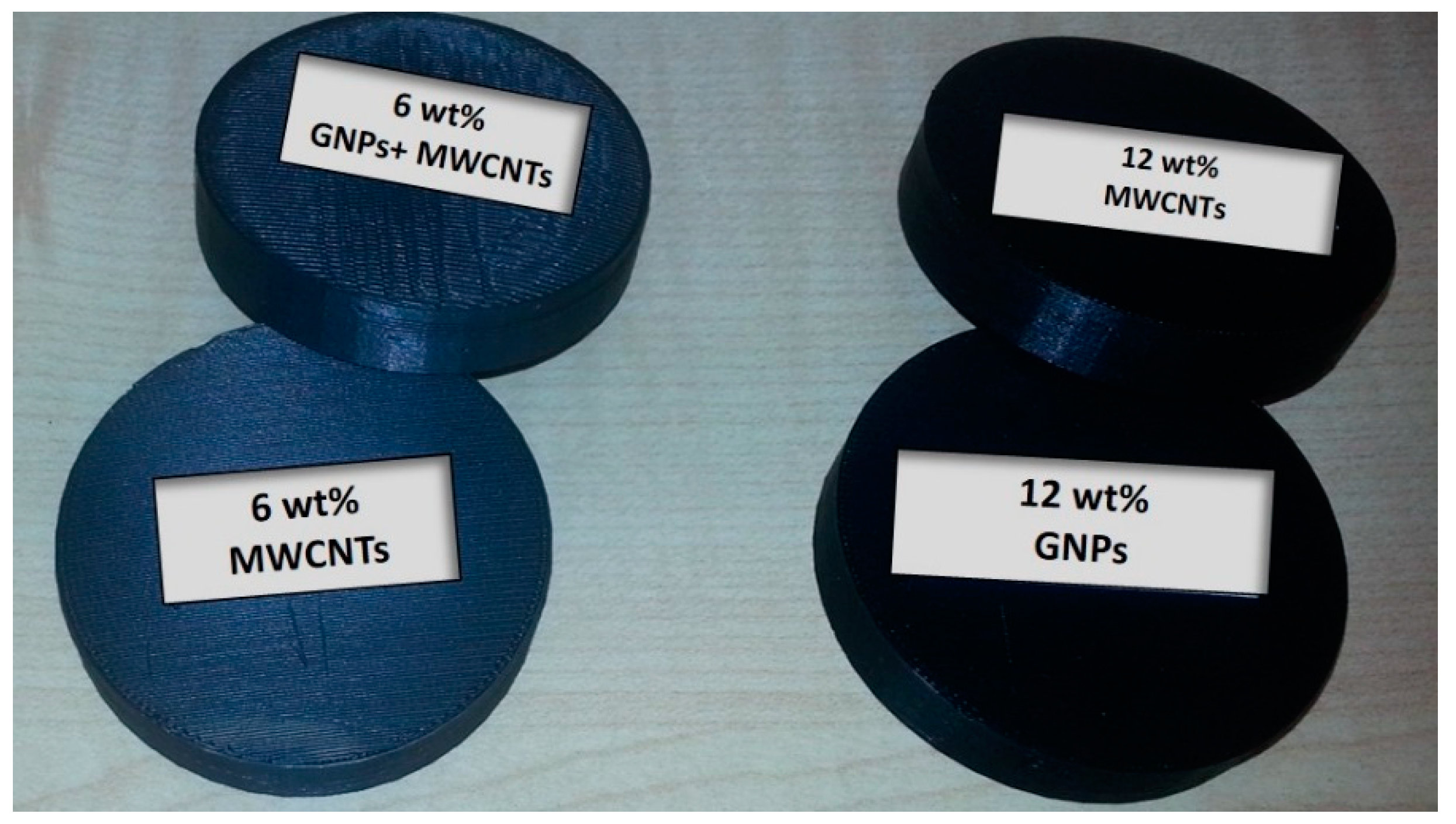
2.1. Preparation of Nanocomposites
2.2. 3D Printing (FDM) for Sample Preparation
2.3. Experimental Methods
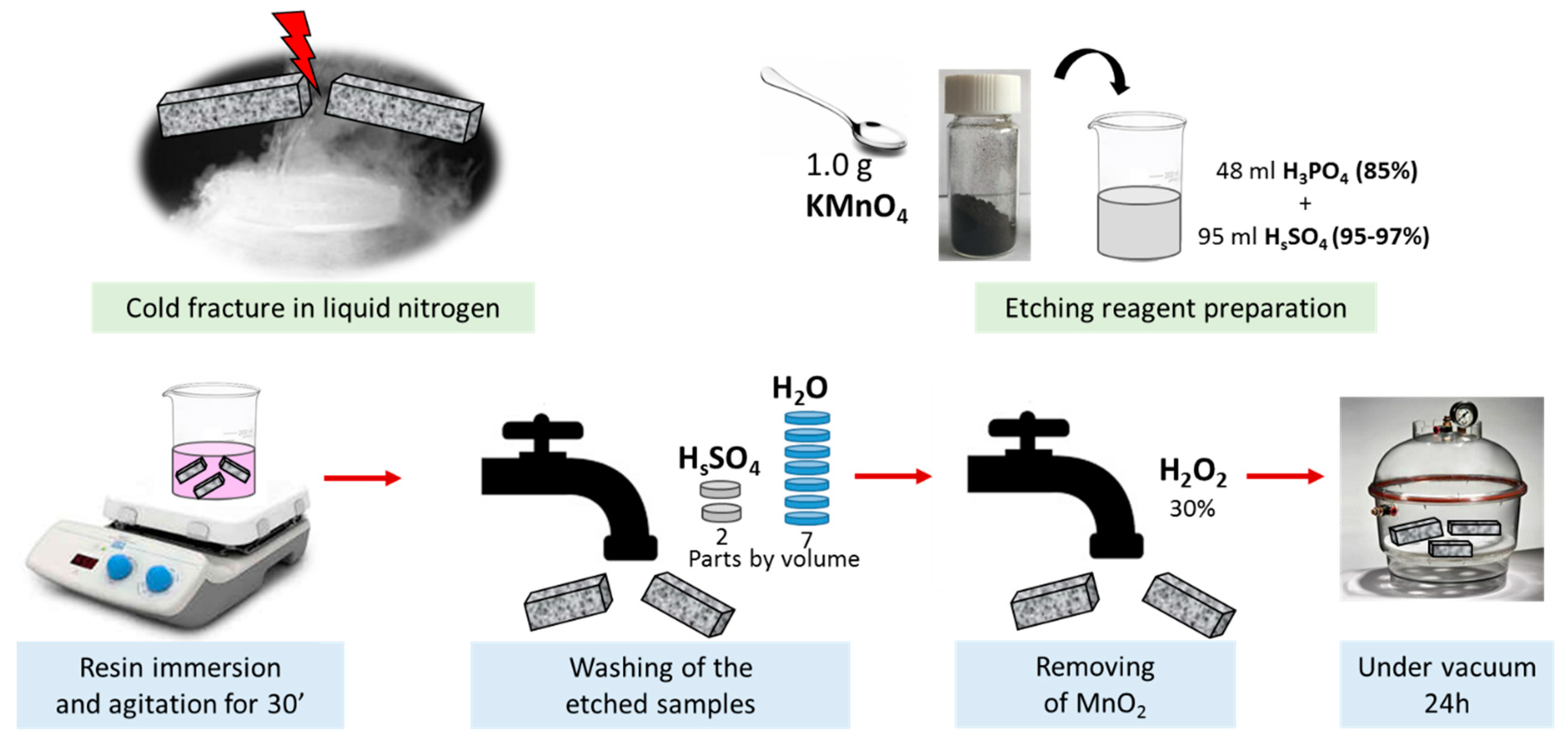
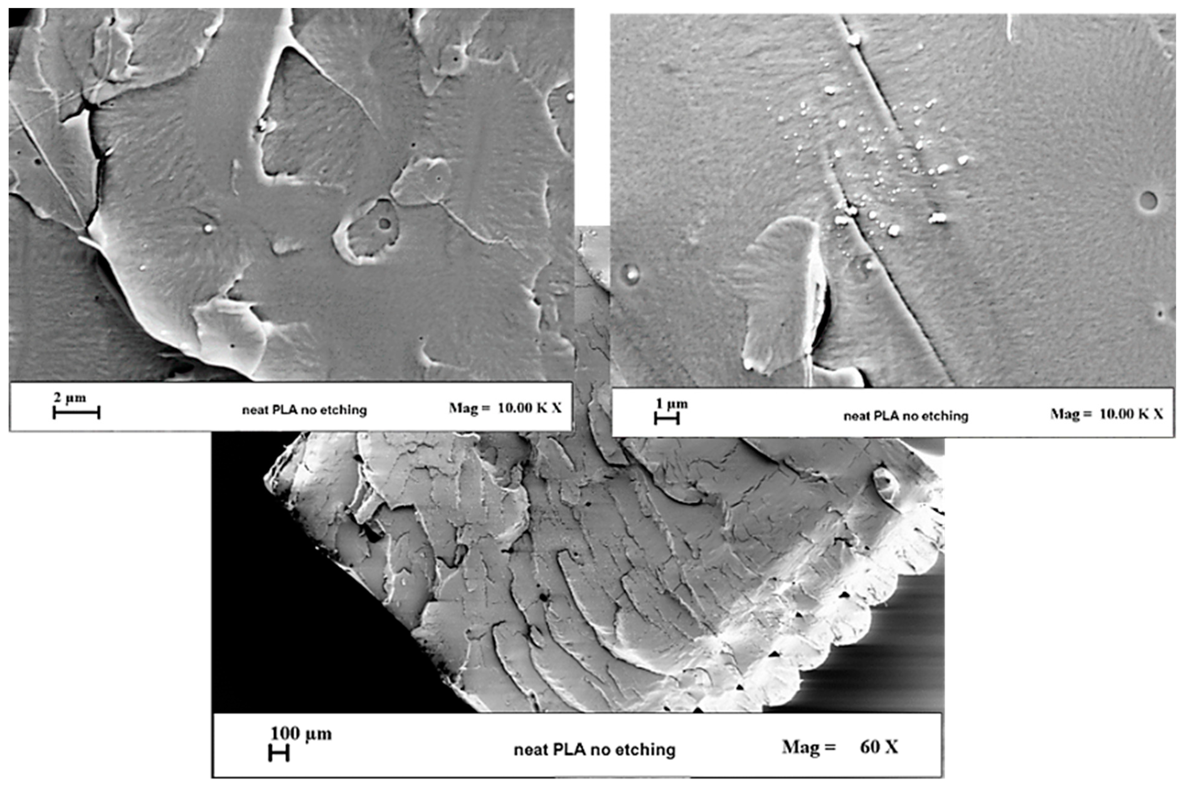
2.3.1. Scanning Electron Microscopy (SEM)
2.3.2. Thermal Measurements
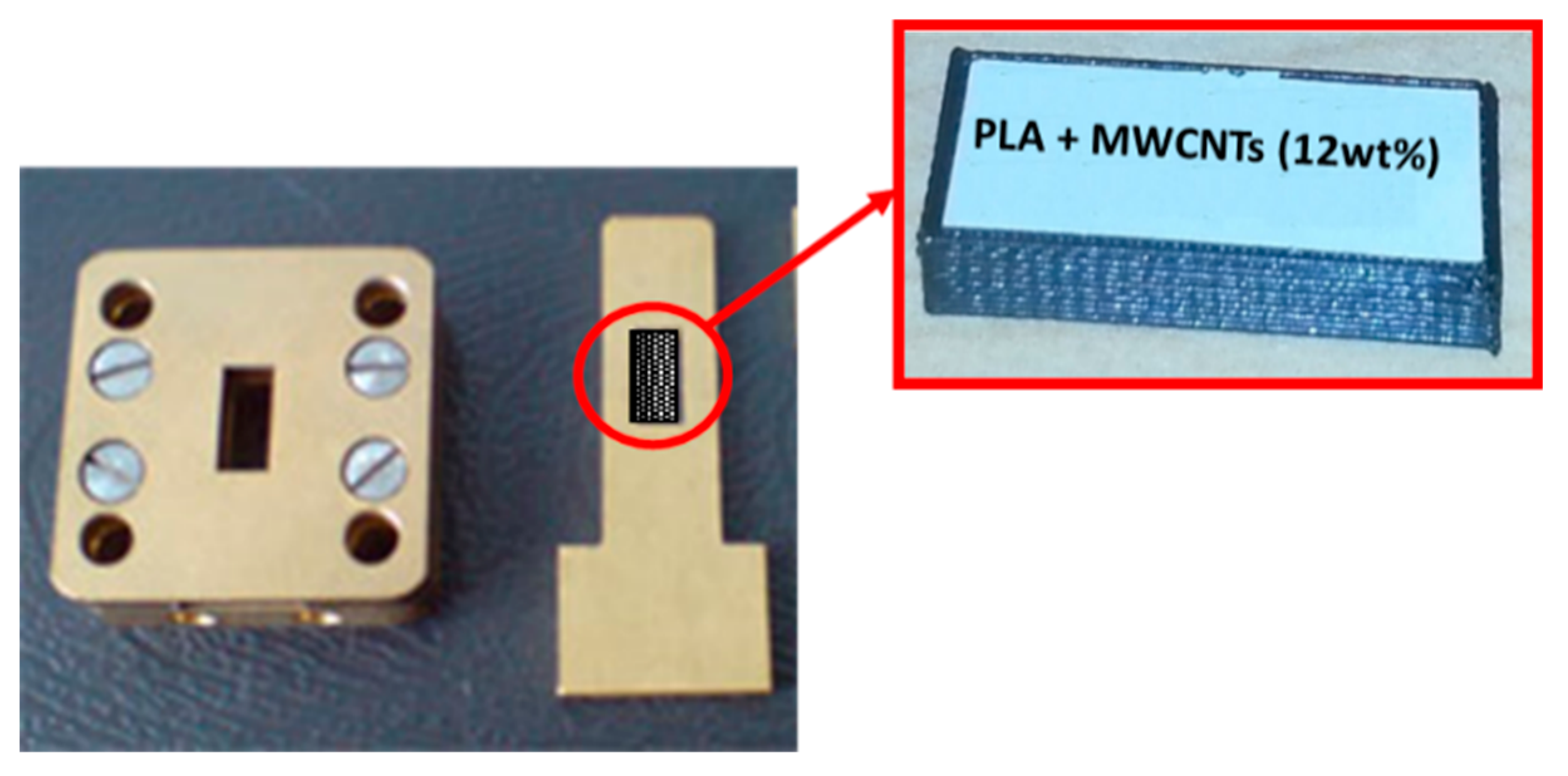
2.3.3. Electrical Measurements
2.3.4. Electromagnetic Measurements
3. Results
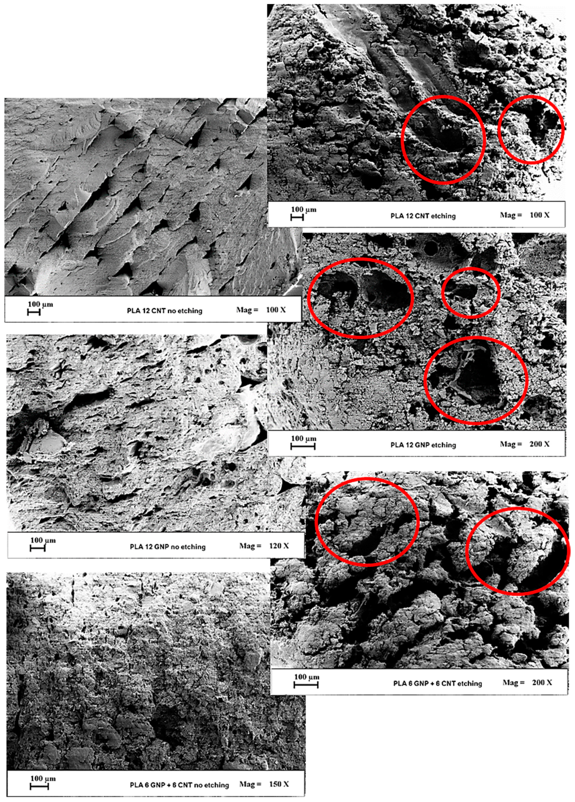
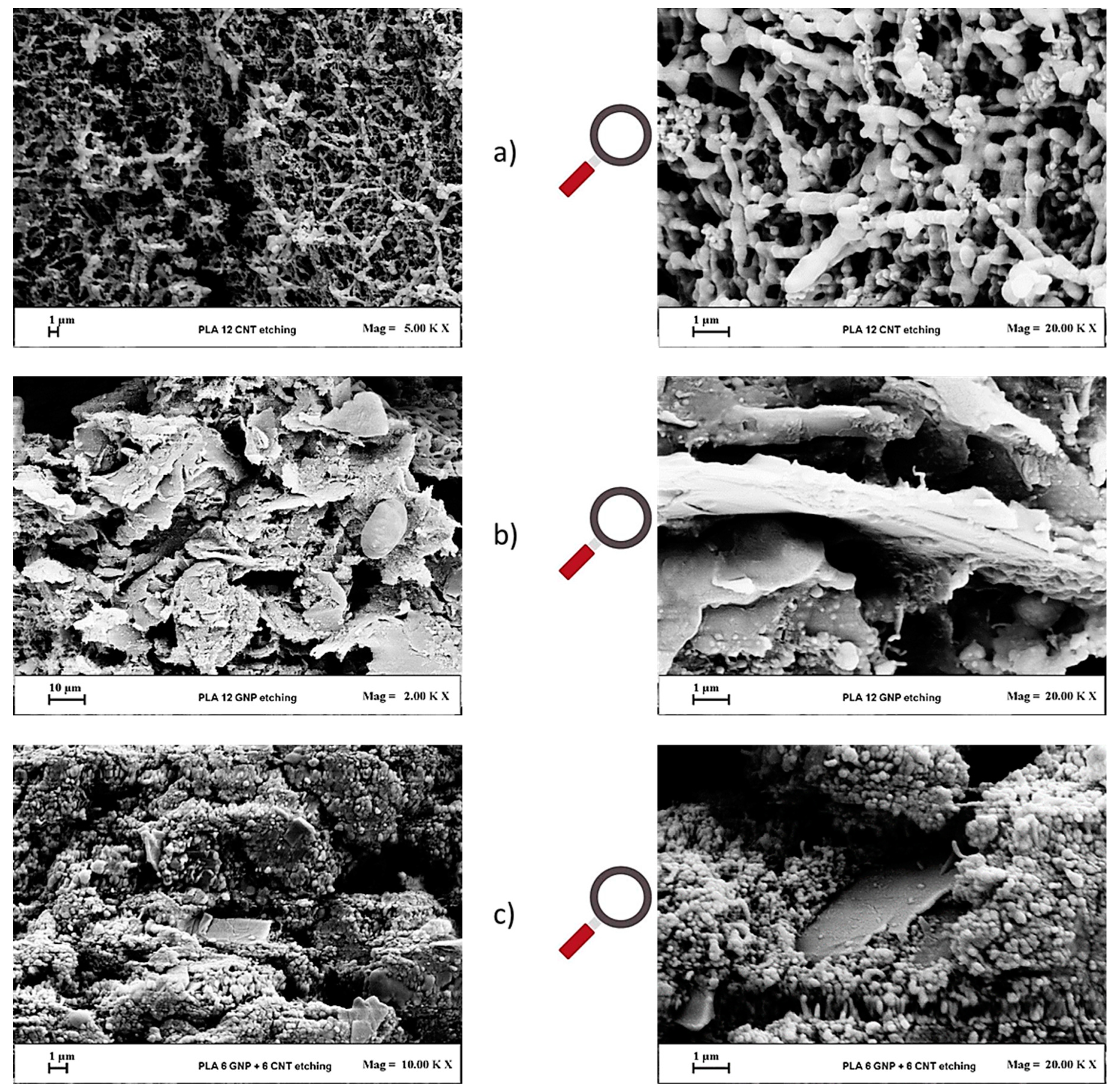
3.1. Morphological Investigation
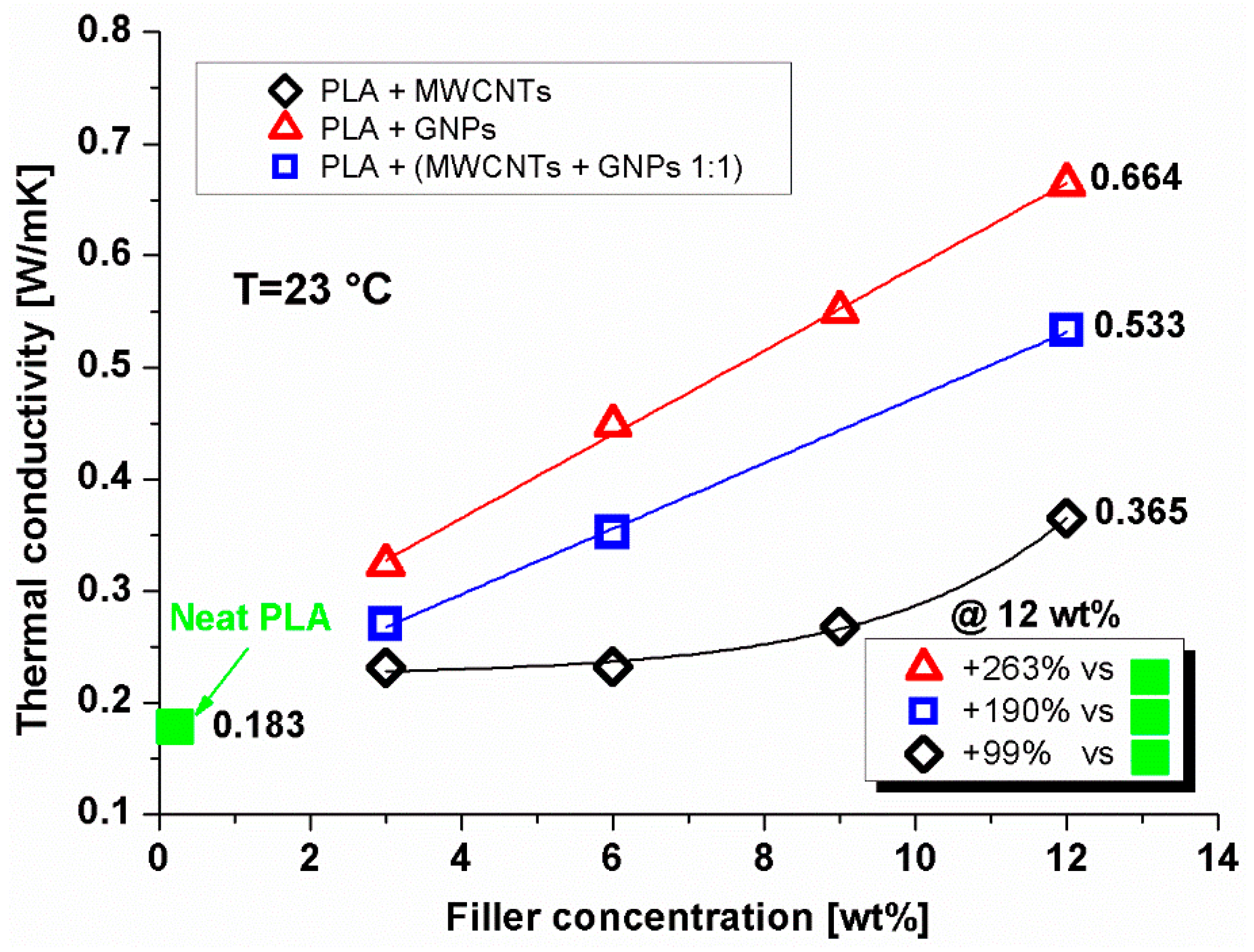
3.2. Thermal Conductivity
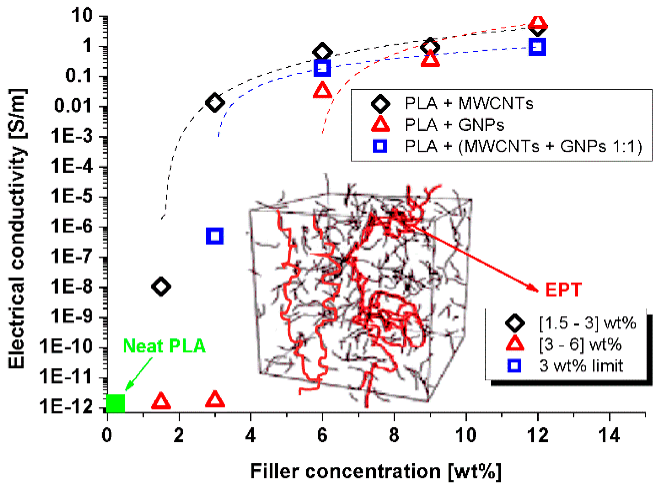
3.3. Preliminary DC Electrical Properties
3.4. Electromagnetic Properties in Ka-Band Frequency Range
3.4.1. Dielectric Spectroscopy
3.4.2. Electromagnetic Properties: Transmission, Reflection, Absorption, and Shielding Efficiency
4. Conclusions
Author Contributions
Funding
Acknowledgments
Conflicts of Interest
References
- Xin, W.; Man, J.; Zuowan, Z.; Jihu, G.; David, H. 3D printing of polymer matrix composites: A review and prospective. Compos. B Eng. 2017, 110, 442–458. [Google Scholar] [CrossRef]
- Ngo, T.D.; Kashani, A.; Imbalzano, G.; Nguyen, K.T.Q.; Hui, D. Additive manufacturing (3D printing): A review of materials, methods, applications and challenges. Compos. B Eng. 2018, 143, 172–196. [Google Scholar] [CrossRef]
- Kruth, J.P.; Leu, M.C.; Nakagawa, T. Progress in additive manufacturing and rapid prototyping. CIRP Ann. 1998, 47, 525–540. [Google Scholar] [CrossRef]
- Wong, K.V.; Hernandez, A. A review of additive manufacturing. ISRN Mech. Eng. 2012, 208760. [Google Scholar] [CrossRef]
- Surange, V.G.; Punit, V.G. 3D printing process using fused deposition modelling (FDM). Int. J. Res. Eng. Technol. (IRJET) 2016, 3, 1403–1406. [Google Scholar]
- Tofail, S.A.; Koumoulos, E.P.; Bandyopadhyay, A.; Bose, S.; O’Donoghue, L.; Charitidis, C. Additive manufacturing: Scientific and technological challenges, market uptake and opportunities. Mater. Today 2018, 21, 22–37. [Google Scholar] [CrossRef]
- Ivanova, O.; Williams, C.; Campbell, T. Additive manufacturing (AM) and nanotechnology: Promises and challenges. Rapid Prototyp. J. 2013, 19, 353–364. [Google Scholar] [CrossRef]
- Rouhollah, D.; Farahani, R.D.; Dubé, M.; Therriault, D. Three-Dimensional Printing of Multifunctional Nanocomposites: Manufacturing Techniques and Applications. Adv. Mater. 2016, 28, 5794–5821. [Google Scholar] [CrossRef]
- Angjellari, M.; Tamburri, E.; Montaina, L.; Natali, M.; Passeri, D.; Rossi, M.; Terranova, M.L. Beyond the concepts of nanocomposite and 3D printing: PVA and nanodiamonds for layer-by-layer additive manufacturing. Mater. Des. 2017, 119, 12–21. [Google Scholar] [CrossRef]
- Viskadourakis, Z.; Vasilopoulos, K.C.; Economou, E.N.; Soukoulis, C.M.; Kenanakis, G. Electromagnetic shielding effectiveness of 3D printed polymer composites. Appl. Phys. A 2017, 123, 736. [Google Scholar] [CrossRef]
- Adams, J.J.; Slimmer, S.C.; Lewis, J.A.; Bernhard, J.T. 3D-printed spherical dipole antenna integrated on small RF node. Electron. Lett. 2015, 51, 661–662. [Google Scholar] [CrossRef]
- Mirzaee, M.; Noghanian, S.; Chang, Y. Low-pro le bowtie antenna with 3D printed substrate. Microw. Opt. Technol. Lett. 2017, 59, 706–710. [Google Scholar] [CrossRef]
- Kim, O.S. 3D printing electrically small spherical antennas. In 2013 IEEE Antennas and Propagation Society International Symposium (APSURSI); IEEE: Piscataway, NJ, USA, 2013; pp. 776–777. [Google Scholar] [CrossRef]
- Ahn, B.Y.; Duoss, E.B.; Motala, M.J.; Guo, X.; Park, S.I.; Xiong, Y.; Yoon, J.; Nuzzo, R.G.; Rogers, J.A.; Lewis, J.A. Omnidirectional Printing of Flexible, Stretchable, and Spanning Silver Microelectrodes. Microw. Opt. Technol. Lett. 2017, 59, 706–710. [Google Scholar] [CrossRef] [PubMed]
- Kestilä, A.; Nordling, K.; Miikkulainen, V.; Kaipio, M.; Tikka, T.; Salmi, M.; Auer, A.; Leskelä, M.; Ritala, M. Towards space-grade 3D-printed, ALD-coated small satellite propulsion components for fluidics. Addit. Manuf. 2018, 22, 31–37. [Google Scholar] [CrossRef]
- Bychanok, D.; Angelova, P.; Paddubskaya, A.; Meisak, D.; Shashkova, L.; Demidenko, M.; Plyushch, A.; Ivanov, E.; Krastev, R.; Kotsilkova, R.; et al. Terahertz absorption in graphite nanoplatelets/polylactic acid composites. J. Phys. D Appl. Phys. 2018, 51, 145307. [Google Scholar] [CrossRef]
- Gnanasekaran, K.; Heijmans, T.; van Bennekom, S.; Woldhuis, H.; Wijnia, S.; de With, G.; Friedrich, H. 3D printing of CNT- and graphene-based conductive polymer nanocomposites by fused deposition modeling. Appl. Mater. Today 2017, 9, 21–28. [Google Scholar] [CrossRef]
- Sagias, V.D.; Giannakopoulos, K.I.; Stergiou, C. Mechanical properties of 3D printed polymer specimens. Procedia Struct. Integr. 2018, 10, 85–90. [Google Scholar] [CrossRef]
- Taufik, M.; Jain, P.K. Role of build orientation in layered manufacturing: A review. Int. J. Manuf. Technol. Manag. 2013, 27, 47–73. [Google Scholar] [CrossRef]
- Flaata, T.; Michna, G.J.; Letcher, T. Thermal conductivity testing apparatus for 3D printed materials. In Proceedings of the ASME 2017 Summer Heat Transfer Conference, Bellevue, WA, USA, 9–12 July 2017. [Google Scholar] [CrossRef]
- Sonsalla, T.; Moore, A.L.; Meng, W.J.; Radadia, A.D.; Weiss, L. 3-D printer settings effects on the thermal conductivity of acrylonitrile butadiene styrene (ABS). Polym. Test. 2018, 70, 389–395. [Google Scholar] [CrossRef]
- Weiss, K.-P.; Bagrets, N.; Lange, C.; Goldacker, W.; Wohlgemuth, J. Thermal and mechanical properties of selected 3D printed thermoplastics in the cryogenic temperature regime. IOP Conf. Ser. Mater. Sci. Eng. 2015, 102, 012022. [Google Scholar] [CrossRef]
- Gao, W.; Zhang, Y.; Ramanujan, D.; Ramani, K.; Yong Chen, Y.; Williams, C.B.; Wange, C.L.; Shin, Y.C.; Zhang, S.; Zavattieri, P.D. The status, challenges, and future of additive manufacturing in engineering. Comput. Aided Des. 2015, 69, 65–89. [Google Scholar] [CrossRef]
- Utela, B.; Storti, D.; Anderson, R.; Ganter, M. A review of process development steps for new material systems in three dimensional printing (3DP). J Manuf Process 2008, 10, 96–104. [Google Scholar] [CrossRef]
- Spinelli, G.; Lamberti, P.; Tucci, V.; Kotsilkova, R.; Tabakova, S.; Ivanova, R.; Angelova, P.; Angelov, V.; Ivanov, E.; Di Maio, R.; et al. Morphological, Rheological and Electromagnetic Properties of Nanocarbon/Poly(lactic) Acid for 3D Printing: Solution Blending vs. Melt Mixing. Materials 2018, 11, 2256. [Google Scholar] [CrossRef] [PubMed]
- Spinelli, G.; Lamberti, P.; Tucci, V.; Ivanova, R.; Tabakova, S.; Ivanov, E.; Kotsilkova, R.; Cimmino, S.; Di Maio, R.; Silvestre, C. Rheological and electrical behaviour of nanocarbon/poly(lactic) acid for 3D printing applications. Compos. B Eng. 2019, 167, 467–476. [Google Scholar] [CrossRef]
- Lamberti, P.; Spinelli, G.; Kuzhir, P.; Guadagno, L.; Naddeo, C.; Romano, V.; Kotsilkova, R.; Angelova, P.; Georgiev, V. Evaluation of Thermal and Electrical Conductivity of Carbon-based PLA Nanocomposites for 3D Printing. AIP Conf. Proc. 2018, 1981, 020158. [Google Scholar] [CrossRef]
- Kotsilkova, R.; Petrova-Doycheva, I.; Menseidov, D.; Ivanov, E.; Paddubskaya, A.; Kuzhir, P. Exploring thermal annealing and graphene-carbon nanotube additives to enhance crystallinity, thermal, electrical and tensile properties of aged poly(lactic) acid-based filament for 3D printing. Compos. Sci. Tech. 2019, 181, 107712. [Google Scholar] [CrossRef]
- Batakliev, T.; Petrova-Doycheva, I.; Angelov, V.; Georgiev, V.; Ivanov, E.; Kotsilkova, R.; Casa, M.; Cirillo, C.; Adami, R.; Sarno, M.; et al. Effects of Graphene Nanoplatelets and Multiwall Carbon Nanotubes on the Structure and Mechanical Properties of Poly(lactic acid) Composites: A Comparative Study. Appl. Sci. 2019, 9, 469. [Google Scholar] [CrossRef]
- Batakliev, T.; Georgiev, V.; Ivanov, E.; Kotsilkova, R.; Di Maio, R.; Silvestre, C.; Cimmino, S. Nanoindentation analysis of 3D printed poly(lactic acid)-based composites reinforced with graphene and multiwall carbon nanotubes. J. Appl. Polym. Sci. 2018, 136, 74260. [Google Scholar] [CrossRef]
- Stoof, D.; Pickering, K. Sustainable composite fused deposition modelling filament using recycled pre-consumer polypropylene. Compos. B Eng. 2018, 135, 110–118. [Google Scholar] [CrossRef]
- Gonçalves, J.; Lima, P.; Krause, B.; Pötschke, P.; Lafont, U.; Gomes, J.R.; Abreu, C.S.; Paiva, M.C.; Covas, J.A. Electrically conductive polyetheretherketone nanocomposite filaments: From production to fused deposition modeling. Polymers 2018, 10, 925. [Google Scholar] [CrossRef]
- Guadagno, L.; Raimondo, M.; Vertuccio, L.; Mauro, M.; Guerra, G.; Lafdi, K.; De Vivo, B.; Lamberti, P.; Spinelli, G.; Tucci, V. Optimization of graphene-based materials outperforming host matrices. RSC Adv 2015, 5, 36969–36978. [Google Scholar] [CrossRef]
- Gustafsson, S.E. Transient plane source techniques for thermal conductivity and thermal diffusivity measurements of solid materials. Rev. Sci. Instrum. 1991, 62, 797–804. [Google Scholar] [CrossRef]
- Ghosh, S.; Teweldebrhan, D.; Morales, J.R.; Garay, J.E.; Balandin, A.A. Thermal properties of the optically transparent pore-free nanostructured yttria-stabilized zirconia. J. Appl. Phys. 2009, 106, 113507. [Google Scholar] [CrossRef]
- Romano, V.; Naddeo, C.; Vertuccio, L.; Lafdi, K.; Guadagno, L. Experimental Evaluation and Modelling of Thermal Conductivity of Tetrafunctional Epoxy Resin Containing Different Carbon Nanostructures. Pol. Eng. Sci. 2017, 57, 779–786. [Google Scholar] [CrossRef]
- (ISO 22007-2:2015), Plastics—Determination of Thermal Conductivity and Thermal Diffusivity—Part 2: Transient Plane Heat Source (Hot Disc) Method; Swedish Standards Institute: Stockholm, Sweden, 2015.
- Dupleix, A.; Kusiak, A.; Hughes, M.; Rossi, F. Measuring the thermal properties of green wood by the transient plane source (TPS) technique. Holzforschung 2012, 67, 1–9. [Google Scholar] [CrossRef]
- Zhang, H.; Li, T.-M.; Tao, W.-Q. Theoretical accuracy of anisotropic thermal conductivity determined by transient plane source method. Int. J. Heat Mass Transf. 2017, 108, 1634–1644. [Google Scholar] [CrossRef]
- Bychanok, D.; Plyushch, A.; Piasotski, K.; Paddubskaya, A.; Voronovich, S.; Kuzhir, P.; Baturkin, S.; Klochkov, A.; Korovin, E.; Letellier, M.; et al. Electromagnetic properties of polyurethane template-based carbon foams in Ka-band. Phys. Scr. 2015, 90, 094019. [Google Scholar] [CrossRef]
- Hone, J.; Whitney, M.; Piskoti, C.; Zettl, A. Thermal conductivity of single-walled carbon nanotubes. Phys. Rev. B 1999, 59, 2514–2516. [Google Scholar] [CrossRef]
- Balandin, A.A. Thermal properties of graphene and nanostructured carbon materials. Nat. Mater. 2001, 10, 569–581. [Google Scholar] [CrossRef]
- Noh, Y.J.; Kim, H.K.; Ku, B.-C.; Khil, M.-S.; Kim, S.Y. Thermal conductivity of polymer composites with geometric characteristics of carbon allotropes. Adv. Eng. Mat. 2016, 18, 1127–1132. [Google Scholar] [CrossRef]
- Kim, S.H.; Bae, H.S.; Yu, J.; Kim, S.Y. Thermal conductivity of polymer composites with geometrical characteristics of graphene nanoplatelets. Sci. Rep. 2016, 6, 26825. [Google Scholar] [CrossRef] [PubMed]
- Yan, H.; Tang, Y.; Lang, W.; Li, Y. Enhanced thermal conductivity in polymer composites with aligned graphene nanosheets. J. Mat. Sci. 2014, 49, 5256–5264. [Google Scholar] [CrossRef]
- Stauffer, D.; Aharony, A. Introduction to Percolation Theory; Taylor & Francis: London, UK, 2003. [Google Scholar]
- De Vivo, B.; Lamberti, P.; Spinelli, G.; Tucci, V. A morphological and structural approach to evaluate the electromagnetic performances of composites based on random networks of carbon nanotubes. J. Appl. Phys. 2014, 15, 154311. [Google Scholar] [CrossRef]
- Nan, C.-W.; Shen, Y.; Ma, J. Physical properties of composites near percolation. Annu. Rev. Mater. Res. 2010, 40, 131–151. [Google Scholar] [CrossRef]
- De Vivo, B.; Lamberti, P.; Spinelli, G.; Tucci, V.; Guadagno, L.; Raimondo, M. The effect of filler aspect ratio on the electromagnetic properties of carbon-nanofibers reinforced composites. J. Appl. Phys. 2015, 118, 064302. [Google Scholar] [CrossRef]
- Urquijo, J.; Dadreou, S.; Echevarria, G.; Eguiazabal, J.I. Morphology and properties of electrically and rheologically percolated PLA/PCL/CNT nanocompoistes. J. Appl. Polym. SCi. 2017, 134, 45265. [Google Scholar] [CrossRef]
- Tamura, R.; Lim, E.; Manaka, T.; Iwamoto, M. Analysis of pentacene field effect transistor as a Maxwell-Wagner effect element. J. Appl. Phys. 2006, 100, 114515. [Google Scholar] [CrossRef]
- Arjmand, M.; Mahmoodi, M.; Park, S.; Sundarara, U.T. An innovative method to reduce the energy loss of conductive filler/polymer composites for charge storage applications. Compos. Sci. Technol. 2013, 78, 24–29. [Google Scholar] [CrossRef]
- Panwar, V.; Park, J.O.; Park, S.H.; Kumar, S.; Mehra, R.M. Electrical, dielectric, and electromagnetic shielding properties of polypropylene-graphite composites. J. Appl. Polym. Sci. 2010, 115, 1306–1314. [Google Scholar] [CrossRef]
- Yuan, J.-K.; Yao, S.-H.; Dang, Z.-M.; Sylvestre, A.; Genestoux, M.; Bai, J. Giant Dielectric Permittivity Nanocomposites: Realizing True Potential of Pristine Carbon Nanotubes in Polyvinylidene Fluoride Matrix through an Enhanced Interfacial Interaction. J. Phys. Chem. C 2011, 115, 5515–5521. [Google Scholar] [CrossRef]
- Ameli, A.; Wang, S.; Kazemi, Y.; Park, C.B.; Pötschke, P. A facile method to increase the charge storage capability of polymer nanocomposites. Nano Energy 2015, 15, 54–65. [Google Scholar] [CrossRef]
- Arjmand, M.; Mahmoodi, M.; Gelves, G.A.; Park, S.; Sundararaj, U. Electrical and electromagnetic interference shielding properties of flow-induced oriented carbon nanotubes in polycarbonate. Carbon 2011, 49, 3430–3440. [Google Scholar] [CrossRef]
- Clayton, R.P. Introduction to Electromagnetic Compatibility; John Wiley & Sons, Inc.: Hoboken, NJ, USA, 2006. [Google Scholar]
- Celozzi, S.; Araneo, R.; Lovatr, G.; Clayton, P. Electromagnetic Shielding; John Wiley & Sons, Inc.: Hoboken, NJ, USA, 2008. [Google Scholar]
- Zhang, Y.; Wang, Z.; Zhang, B.; Zhao, G.-L.; Guo, S.M. The electromagnetic interference shielding effectiveness of high aspect-ratio SiC nanofibers/epoxy composites. RSC Adv. 2015, 5, 93499–93506. [Google Scholar] [CrossRef]
- De Vivo, B.; Lamberti, P.; Spinelli, G.; Tucci, V.; Guadagno, L.; Raimondo, M.; Vertuccio, L.; Vittoria, V. Improvement of the electrical conductivity in multiphase epoxy-based MWCNT nanocomposites by means of an optimized clay content. Comp. Sci. Technol. 2013, 89, 69–76. [Google Scholar] [CrossRef]


| Property | Phase | ||
|---|---|---|---|
| Polymer | GNP | MWCNT-OH | |
| Commercial code | PLA-3D850 | TNIGNP | TNIMH4 |
| Purity (wt %) | x | 90 | 95 |
| Thickness (nm) | x | <30 | x |
| Peak melt temperature (°C) | 165–180 | x | x |
| Glass transition Temp. (°C) | 55–60 | x | x |
| MFR, g/10 min * | 7–9 | x | x |
| Average size (µm) | x | 5–7 | x |
| External diameter, (nm) | x | x | 10–30 |
| Length (µm) | x | x | 10–30 |
| OH-content (%) | x | x | 2.48 |
| Aspect ratio | x | ~240 | ~1000 |
| Density (g/cm3) | x | 2.2 | 2.1 |
| Filler (wt %) |  Neat PLA | Δ PLA + GNPs | ◊ PLA + MWCNTs |  PLA + (MWCNTs + GNPs 1:1) |
|---|---|---|---|---|
| 0 | 0.183 | x | x | x |
| 3.0 | x | 0.323 | 0.231 | 0.270 |
| 6.0 | x | 0.448 | 0.232 | 0.352 |
| 9.0 | x | 0.550 | 0.268 | x |
| 12.0 | x | 0.664 | 0.365 | 0.533 |
| Filler (wt %) | Neat PLA | Δ PLA+GNPs | ◊ PLA+MWCNTs | PLA+(MWCNTs+GNPs 1:1) |
|---|---|---|---|---|
| 0 | 1 × 10⁻¹² | x | x | x |
| 1.5 | x | 1.50 × 10⁻¹² | 1.08 × 10⁻⁸ | x |
| 3.0 | x | 1.70 × 10⁻¹² | 1.40 × 10⁻² | 5.02 × 10⁻⁷ |
| 6.0 | x | 3.12 × 10⁻² | 6.57 × 10⁻¹ | 1.85 × 10⁻¹ |
| 9.0 | x | 3.47 × 10⁻¹ | 9.40 × 10⁻¹ | x |
| 12.0 | x | 6.27 | 4.54 | 9.50 × 10⁻¹ |
| Composite | T | R | A | SE (dB) | SE (%) |
|---|---|---|---|---|---|
| Neat PLA | 0.96 | 0.02 | 0.02 | 0.20 | 4 |
| Δ PLA+GNPs | 0.09 | 0.71 | 0.19 | 10.22 | 89 |
| ◊ PLA+MWCNTs | 0.09 | 0.71 | 0.19 | 10.22 | 89 |
| PLA+(MWCNTs+GNPs 1:1) | 0.05 | 0.79 | 0.16 | 13.45 | 95 |
© 2019 by the authors. Licensee MDPI, Basel, Switzerland. This article is an open access article distributed under the terms and conditions of the Creative Commons Attribution (CC BY) license (http://creativecommons.org/licenses/by/4.0/).
Share and Cite
Spinelli, G.; Lamberti, P.; Tucci, V.; Kotsilkova, R.; Ivanov, E.; Menseidov, D.; Naddeo, C.; Romano, V.; Guadagno, L.; Adami, R.; et al. Nanocarbon/Poly(Lactic) Acid for 3D Printing: Effect of Fillers Content on Electromagnetic and Thermal Properties. Materials 2019, 12, 2369. https://doi.org/10.3390/ma12152369
Spinelli G, Lamberti P, Tucci V, Kotsilkova R, Ivanov E, Menseidov D, Naddeo C, Romano V, Guadagno L, Adami R, et al. Nanocarbon/Poly(Lactic) Acid for 3D Printing: Effect of Fillers Content on Electromagnetic and Thermal Properties. Materials. 2019; 12(15):2369. https://doi.org/10.3390/ma12152369
Chicago/Turabian StyleSpinelli, Giovanni, Patrizia Lamberti, Vincenzo Tucci, Rumiana Kotsilkova, Evgeni Ivanov, Dzhihan Menseidov, Carlo Naddeo, Vittorio Romano, Liberata Guadagno, Renata Adami, and et al. 2019. "Nanocarbon/Poly(Lactic) Acid for 3D Printing: Effect of Fillers Content on Electromagnetic and Thermal Properties" Materials 12, no. 15: 2369. https://doi.org/10.3390/ma12152369
APA StyleSpinelli, G., Lamberti, P., Tucci, V., Kotsilkova, R., Ivanov, E., Menseidov, D., Naddeo, C., Romano, V., Guadagno, L., Adami, R., Meisak, D., Bychanok, D., & Kuzhir, P. (2019). Nanocarbon/Poly(Lactic) Acid for 3D Printing: Effect of Fillers Content on Electromagnetic and Thermal Properties. Materials, 12(15), 2369. https://doi.org/10.3390/ma12152369