1. Introduction
The human brain’s neocortex covers the brain’s surficial area, which is known to carry out the most intelligence functions. The thickness of neocortex has been observed as thin as 2.5 mm, where six layers are stacked one-by-one [
1,
2,
3]. The six neocortical layers seem to be columnar, in which the complicated vertical and horizontal synaptic connections are intertwined among neurons to form the 3-dimensional neuronal architecture [
4,
5]. The neocortical neurons collectively respond to human’s sensory information from retina, cochlea, and olfactory organ [
6]. The collective activation of neocortical neurons are trained over and over with respect to time, by changing the synaptic connection’s strength according to the sensory stimuli. The neuronal activation and synaptic plasticity can be thought of as a fundamental aspect of human perception and cognition, which are computed in a different way from the conventional Von Neumann machines.
As a software framework, Hierarchical Temporal Memory (HTM) has been developed to model the cognitive functions of neocortex [
7,
8,
9,
10,
11]. By doing so, HTM can recognize and interpret various spatiotemporal patterns, mimicking how the human brain’s neocortex understands human’s sensory stimuli. The software framework of HTM is divided into two functional blocks: Spatial Pooler (SP) and Temporal Memory (TM). The role of SP is receiving and learning the sensory information. In SP, the sensory information is transformed into the collective activation of neocortical neurons. From the biological experiments, the neocortical neurons have been observed to be activated sparsely, not densely, in response to human sensory stimuli. The sparse activation of neocortical neurons is mathematically described as Sparse Distributed Representation (SDR) in HTM [
1]. After SP learning the spatial features of the sensory stimuli, TM responds to the temporal sequences of SDR patterns generated from SP. By learning the temporal sequences of SDR patterns, TM can perform recognition and prediction for them.
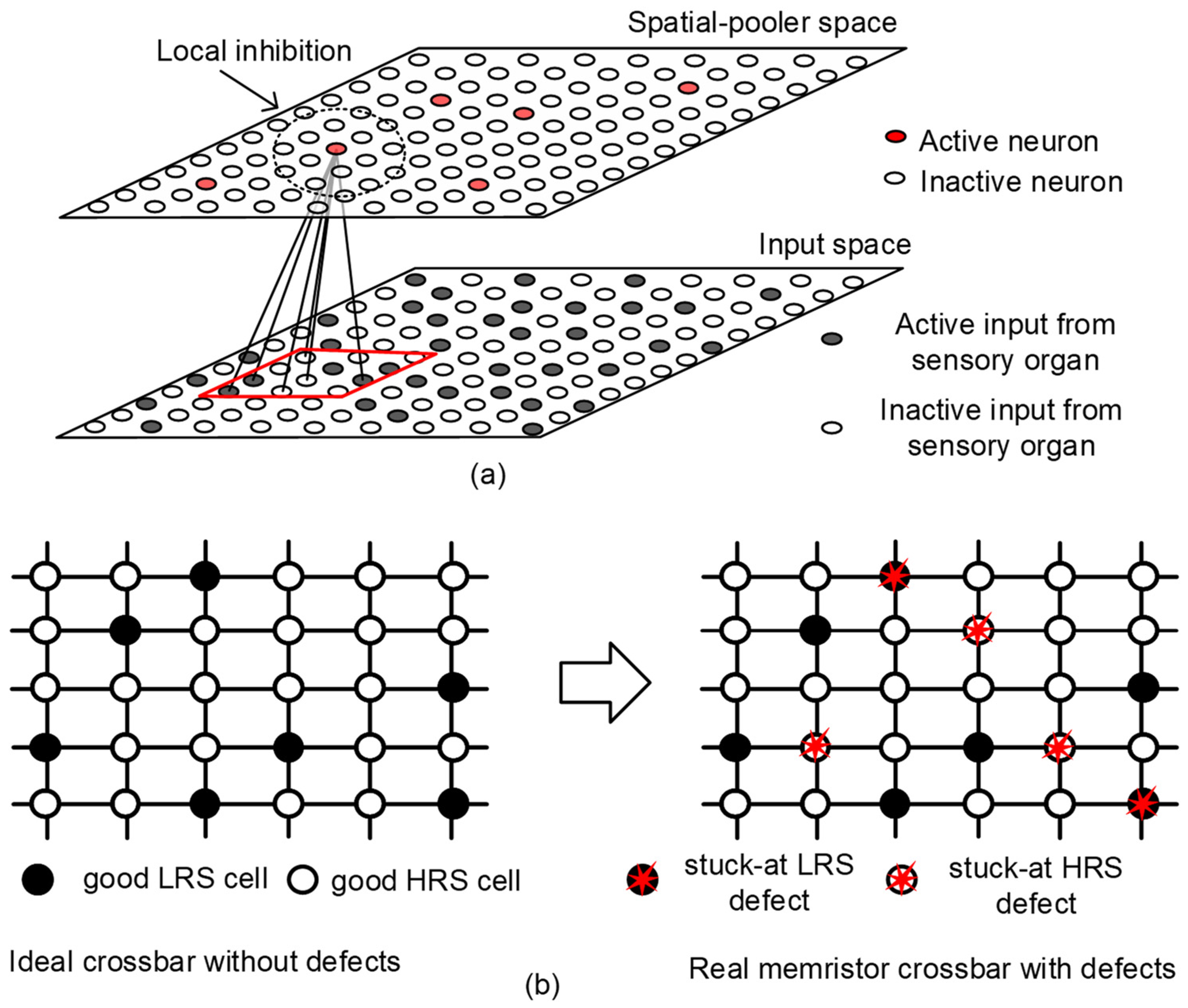
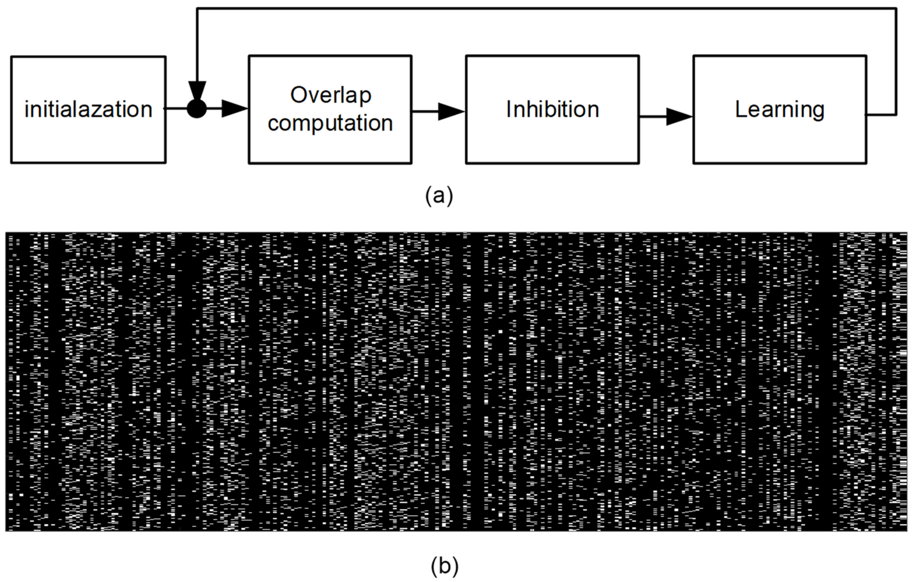
Figure 1a shows a conceptual diagram of SP operation, where the input-space neurons are mapped to the SP neurons [
8]. Here, the input-space and SP neurons refer to the neurons of sensory organ and neocortex, respectively. The sensory stimuli generated from the input-space neurons are connected with the neocortical neurons, as indicated in
Figure 1a. The lines between the input and the SP spaces represent the synaptic connections. Synaptic weights of the connections are trained according to Hebbian learning rule in HTM [
8]. If an SP neuron becomes active, in response to an input-space stimulus, the synaptic weights belonging to this neuron are strengthened, and weakened otherwise [
8]. The circle zone in the SP space represents a local inhibition area, within which only few neurons are allowed to be active. In HTM, the size of inhibition zone in the SP space can be decided to control the sparsity of neuronal activation. It has been known that the percentage of neuronal activation is as sparse as 2% on average in the brain’s neocortex. This low sparsity of neuronal activation may have something to do with high energy-efficiency of neocortical cognitive operation.
In the previous publications, we developed hybrid CMOS-memristor circuits for implementing HTM, which was developed as the software framework originally, as mentioned earlier [
12,
13]. Memristors have been studied intensively for many years for their potential in neuromorphic hardware, since the first experimental demonstration [
14,
15]. This is because the memristive behaviors seem very similar with the experimental synaptic plasticity observed from biological neurons. From the biological experiments, the synaptic connections have been observed to be strengthened or weakened dynamically by electrical spiking signals applied to them [
16].
Moreover, memristors can be fabricated to build 3-dimensional crossbar architecture using the CMOS-compatible Back-End-Of-Line (BEOL) process [
17,
18]. The 3-dimensional connectivity of memristor-synapses is very similar to the anatomical structure of the biological neocortex. In terms of cognitive functions, the memristor crossbar can perform vector-matrix multiplications in parallel, which can be considered very important in implementing energy-efficient computing like human brain’s cognition, unlike the state-of-the-art Von Neumann based computers [
19,
20].
One important thing to consider in the memristor crossbar is defects, as shown in
Figure 1b. In the real memristor crossbar, there are stuck-defects, such as stuck-at-0, stuck-at-1, etc. [
21]. In addition, variation-related defects can also be considered, where each memristor can have different LRS and HRS values due to process variations [
22]. Here, LRS and HRS mean Low Resistance State and High Resistance State, respectively.
Figure 1b compares the ideal crossbar (without defects) and the real one (with defects). The solid and open red circles with stars represent stuck-at-LRS and stuck-at-HRS defects, respectively. For the memristor defects such as stuck-at-faults and variations, these defects may be caused from the random nature of filamentary current path which can be formed or erased by the applied current and voltage to the memristor. The filamentary current path created or erased during the memristor programming can have statistical distributions like FLASH memory. Various statistical distributions by device-to-device, wafer-to-wafer, lot-to-lot, and process-to-process lead to the variations in memristance and stuck-at-faults [
21].
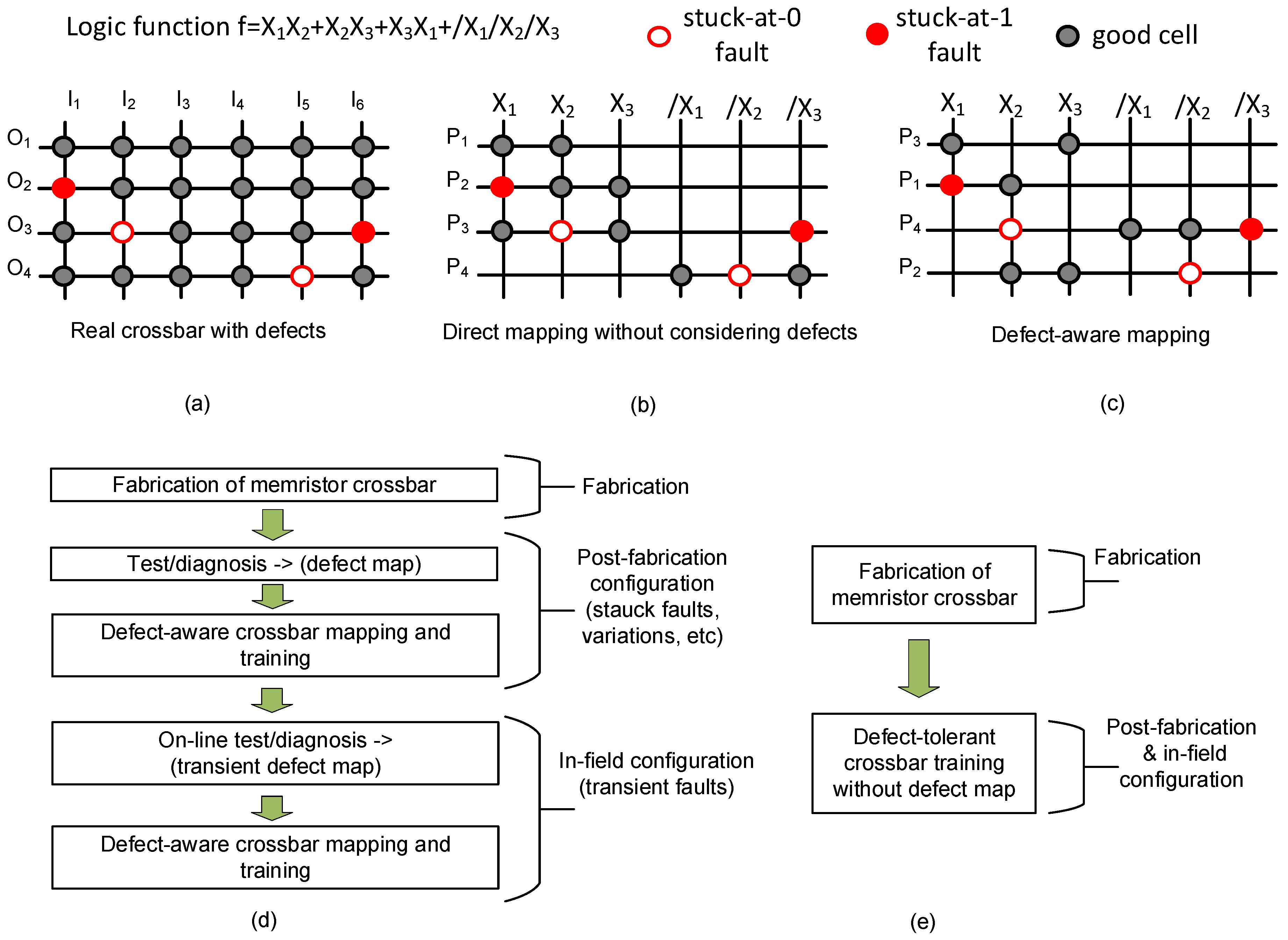
To minimize a loss of recognition rate due to these memristor defects, we can consider the defect-tolerance scheme based on the conventional defect-aware mapping [
21]. To explain the previous defect mapping scheme, the following logic function is assumed,
is implemented in the crossbar [
21].
In the logic function, /X
1 means the inversion of X
1.
Figure 2a shows the real memristor crossbar (with defects). Here, I
1, I
2, etc. represent input columns. O
1, O
2, etc. are output rows. The gray circle indicates a good memristor cell, which can be programmed with HRS or LRS. The solid and open red circles represent stuck-at-1 and stuck-at-0 defects, respectively.
Figure 2b shows the direct mapping without considering the defect map. P
1, P
2, P
3, and P
4 indicate the first, second, third, and fourth partial products in the target logic function. P
1 calculates X
1X
2. However, P
2 calculates X
1X
2X
3, not X
2X
3 defined in the logic function, because of the stuck-at-1 fault on the crossing point between X
1 and P
2. P
4 also calculates the wrong partial product. The stuck-at-0 fault is found at the crossing point between /X
2 and P
4. By doing so, P
4 calculates /X
1/X
3 instead of the target product of /X
1/X
2/X
3.
Figure 2c shows the defect-aware mapping, where the defects can be used in implementing the logic function according to the defect type and location. To do so, the crossbar’s rows in
Figure 2c are reordered to consider the defect type and location in calculating the partial products. For example, the first row in
Figure 2c is assigned to P
3, not P
1. P
1 is assigned to the second row to calculate X
1X
2. The stuck-at-1 fault on the second row can be used in calculating P
1 = X
1X
2. Similarly, the stuck-at-1 fault on P
4 can be employed to calculate P
4 = /X
1/X
2/X
3. Moreover, the stuck-at-0 faults on P
2 and P
4 do not cause a wrong result for the calculation of partial products of P
2 and P
4. As shown in
Figure 2c, the defects can be employed in implementing the target logic function according to the defect type and location. However, the defect-aware mapping scheme demands very complicated circuits, such as memory, processor, controller, etc., to be implemented in hardware.
Figure 2d shows the flowchart of crossbar training using the conventional defect-aware mapping. After fabricating the memristor crossbar, the defect map should be obtained by measuring the crossbar. As a post-fabrication configuration, the trained synaptic weighs can be transferred to the crossbar using the defect-aware mapping, as explained in
Figure 2c. To do so, however, the complicated digital circuits, such as memory, controller, processor, etc., are needed for implementing the defect-aware mapping in hardware, as mentioned earlier.
Not using the defect-aware mapping, in this paper, we propose a simple memristor-CMOS hybrid circuit of defect-tolerant spatial-pooling, which does not need the complicated circuits of memory, controller, processor, etc., as shown in
Figure 2e, where, unlike in
Figure 2d, the crossbar’s defect map is not used. For developing the hybrid circuit of memristor-CMOS, we first show that the spatial-pooling based on Hebbian learning can be defect-tolerant, owing to the boost-factor adjustment, in
Section 2. Additionally, we propose a new memristor-CMOS hybrid circuit, where the winner-take-all circuit is implemented not using capacitors occupying large area. In
Section 3, the proposed hybrid circuit is verified to be able to recognize well Modified subset of National Institute of Standards and Technology (MNIST) hand-written digits, in spite of memristor defects such as stuck-at-faults, variations, etc. In
Section 4, we discuss and compare the following three cases: (1) Spatial-pooling without both the boost-factor adjustment and the defect-aware mapping, (2) spatial-pooling with the defect-aware mapping, and (3) spatial pooling with the boost-factor adjustment, in terms of hardware implementation, energy consumption, and recognition rate. Finally, in
Section 5, we summarize this paper.
2. Materials and Methods
To develop a memristor-CMOS hybrid circuit for realizing HTM’s SP function by hardware, memristor defects such as stuck-at-faults and variations should be considered. To consider the memristor defects in developing the hybrid circuit of the SP function, we explain the memristor fabrication and its behavioral model in the following sub-section of ‘a. Materials’. Then, we describe the boost-factor adjustment in HTM’s SP operation can make it defect-tolerant, because the false activation of defective columns in the crossbar are suppressed, in the sub-section of ‘b. Methods (scheme)’. In the sub-section of ‘c. Method (circuit)’, we propose the memristor-CMOS hybrid circuit by explaining its schematic and operation in detail. The hybrid circuit with the boost-factor adjustment is discussed and compared with the previous techniques without the boost-factor adjustment, later in this paper. The simulation result and comparison indicates that the memristor-CMOS hybrid circuit with the boost-factor adjustment can improve the recognition rate by more than ~20%, than the previous defect-map-based technique. This hybrid circuit can be very useful for energy-efficient computing in future IoT systems, where many IoT sensors are connected to a cloud of centralized data processing, as explained later.
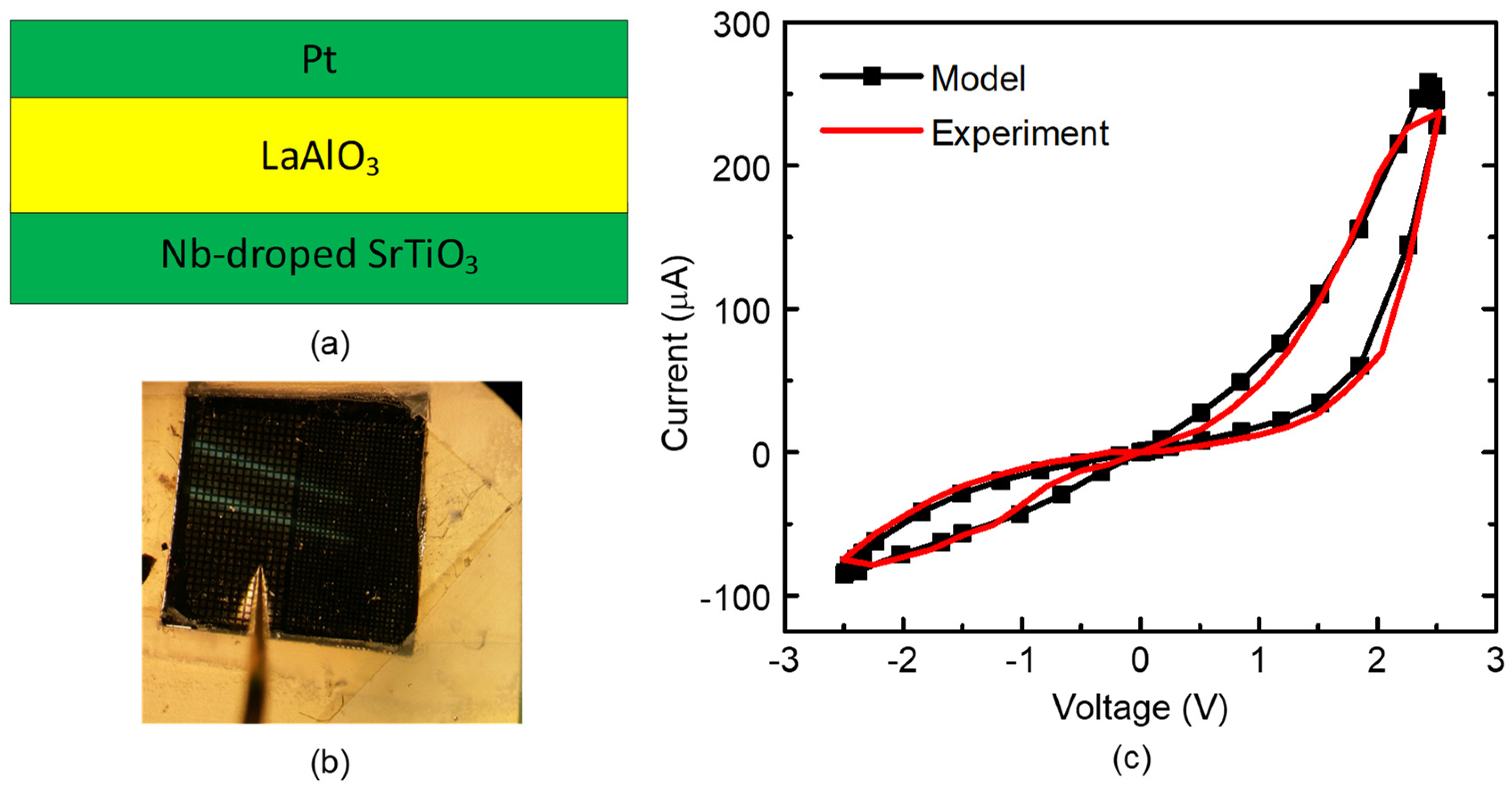
a. Materials
Figure 3a shows a cross-sectional view of the fabricated memristor in this paper. The fabricated memristor has a film structure made of a Pt/LaAlO
3/Nb-doped SrTiO
3 stacked layer [
23]. A microscope picture of the measured device is shown in
Figure 3b, where the top electrode area is 100 µm × 100 µm [
24]. The top and bottom electrodes were formed by Platinum (Pt) and SrTiO3, in the measured device, respectively [
23].
Figure 3c shows current–voltage relationships of the fabricated memristor and the Verilog-A model, respectively [
23]. The measurement was performed by Keithley-4200 (Semiconductor Characterization System, Tektronix, Inc., Beaverton, OR, USA) [
23]. Here, the HRS/LRS ratio in
Figure 3c was observed as large as 100. The black and red lines in
Figure 3c represent the behavioral model of memristors and the measured data, respectively. The behavioral model described by Verilog-A in
Figure 3c was used in the circuit simulation of the memristor-CMOS hybrid circuit in this paper.
b. Methods (scheme): boost-factor adjustment scheme for defect-tolerant spatial-pooling
The spatial-pooling in HTM software framework is composed of initialization, overlap computation, inhibition, and learning, as shown in
Figure 4a [
8,
12]. After the initialization step (Phase 1), three steps: Overlap computation (Phase 2), inhibition (Phase 3), and learning (Phase 4), are repeated sequentially [
8,
12]. In Phase 1, random sets of inputs are selected from the input space, as indicated in
Figure 1a. The number of random sets of inputs per training vector is the same with the number of crossbar’s columns. Each input in this random set can be connected to an output neuron in the SP via a synapse [
8,
12]. In Phase 2, an amount of overlap of each output neuron with the chosen set of inputs from the input space is calculated [
8,
12] The amount of overlap of each neuron in the SP can be calculated with the number of the connected synapses with the active inputs, multiplied by each column’s boost factor. In Phase 3, we decide which columns can be winners within the inhibition radius [
8,
12]. By doing so, the sparsity regarding the percentage of activation in the neocortical neurons can be controlled to not exceed a certain limit. In the case of the human brain’s neocortex, only 2% of neocortical neurons have been observed to be activated in response to human sensory stimuli. In Phase 4, Hebbian learning is performed to strengthen and weaken synaptic connections [
8,
12]. For the winners chosen in Phase 3, the synaptic permanence values for the active inputs are increased by p+. For the inactivate inputs, the permanence values are decreased by p-. p+ and p- represent the increment and decrement of synaptic permanence, respectively. The permanence value is allowed to vary between 0 and 1. If it reaches 1 or 0, the synaptic weight is changed to LRS or HRS, respectively.
One more parameter needed to be updated after the activation of each neuron is a boost factor. The boost factor can be defined with the following inverse relationship with the activity ratio [
8]:
Here, b
i means the boost factor of column, i. β is a positive parameter that controls the strength of the adaptation effect. a
i is the activity ratio of column i, and < a
i, neighbor > means the average activity ratio of the column’s neighborhood. For given M test vectors, the activity ratio of column, i, can be calculated with
Here, ai is the activity ratio of column i. M is the number of test vectors. The activation function defined with ‘activation(column, i)’ in Equation (2) becomes one, if the column, i, is activated. If the column is not activated, the activation function should be zero. For a neuron activated very frequently, its boost factor should be adjusted to be very small to lower the probability of activation. On the contrary, if a neuron is chosen very rarely, its boost factor should be increased. As explained just earlier, by adjusting each column’s boost factor according to each column’s activity ratio, the number of activations can be distributed more evenly for all columns in the crossbar.
We now discuss how each column’s activity ratio can be affected by memristor defects.
Figure 4b shows a defect map of 400 × 256 memristor crossbar. Here, we assume random defects = 10% in the crossbar. The random defects can be stuck-at-HRS and stuck-at-LRS. Because the HRS defects do not cause erroneous activation of neurons, we focus on the LRS defects here.
In
Figure 5a, the number of defects per column is ranked from the largest to the smallest. The number of columns in the crossbar is assumed to be 256 in
Figure 5a. Each column is assumed to have 400 cells. Among the 400 cells per column, the most defective column has almost ~90 defects. The smallest number of defects per column is ~0.
Figure 5b and c compare the simulated boost factors of the crossbars without and with the boost-factor adjustment, respectively. In
Figure 5b, all 256 columns have the same boost factor, fixed by 50. On the contrary, in
Figure 5c, each column’s boost factor is adjusted between 0 and 100, according to each column’s activity ratio.
Figure 5d and e compare the activity ratios of the crossbars without and with the boost-factor adjustment. Here, each column’s activity ratio is shown on the y-axis with respect to the ranked column number according to the number of defects.
Figure 5d clearly indicates that a large number of defects in a defective column causes frequent activation of the column. The small number of defects results in the rare activation of the column. The frequent activation due to the defective column is very likely to be false and should be suppressed not to happen.
Figure 5e shows that the frequent activation of the defective columns can be suppressed, by decreasing the boost factor of the defective columns lower than the neighbors. By doing so, we can reduce the false activation of the defective columns. Thus, the recognition rate loss due to the defective columns can be minimized by the boost-factor adjustment.
In
Figure 5f, the crossbar’s entropy is compared without and with the boost-factor adjustment. The entropy of the crossbar with N columns is calculated with Equation (3) [
8].
In Equation (3), ‘Entropy’ means the calculated amount of entropy. N is the number of columns in the crossbar. a
i is the activity ratio of column i. ‘log’ means the logarithmic function.
Figure 5f indicates that the crossbar with the boost-factor adjustment shows much larger entropy than the crossbar without the boost-factor adjustment. The better entropy can result in a better recognition rate, as shown later in this paper.
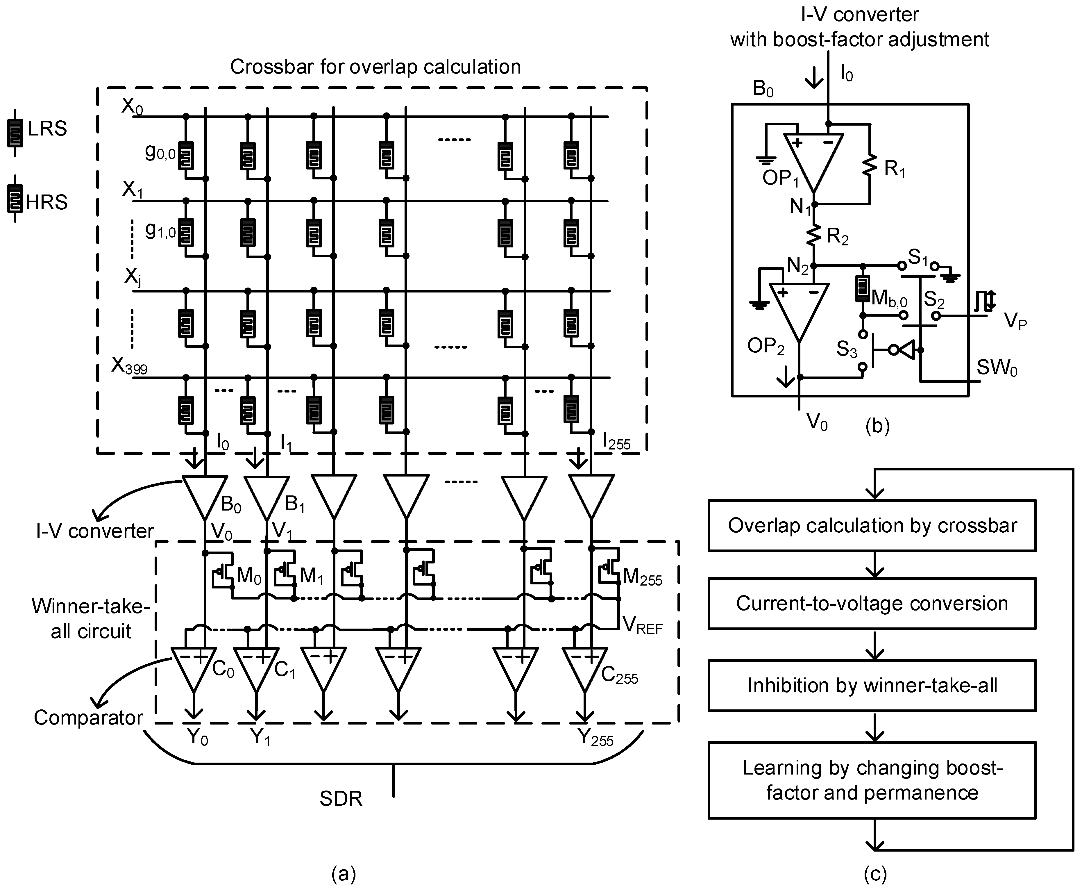
c. Methods (circuit): memristor-CMOS hybrid circuit of defect-tolerant spatial pooling
Figure 6a shows a schematic of the memristor-CMOS hybrid circuit of defect-tolerant spatial pooling, where each column’s boost factor can be adjusted to make each column’s activity ratio more even. The memristor crossbar is composed of 400 rows and 256 columns for recognizing the MNIST hand-written digits. The 400 rows can receive 20 × 20 input pixels of each MNIST test vector. The 256 columns correspond to the 256 output neurons of the SP. In
Figure 6a, X
0 and X
1 are the first and second row, respectively. g
0,0 means memristor’s conductance of row #0 and column #0. Similarly, g
1,0 means memristor’s conductance of row, #1, and column, #0. I
0 and I
1 represent the currents of columns, #0 and #1, respectively. I
0 and I
1 enter the current–voltage converters of B
0 and B
1, respectively, where each column’s boost factor can be adjusted according to each column’s activity ratio. Here, V
0 and V
1 are the converted voltages of columns #0 and #1, respectively. The converted voltages, V
0 and V
1, enter the comparators of C
0 and C
1, respectively, where V
0 and V
1 are compared with V
REF. V
REF is obtained from the maximum output voltage among the neighbors using the diode-connected MOSFETs of M
0, M
1, etc. If we assume the diode ‘ON’ voltage is very small, V
REF can be very similar with the maximum voltage among all the output voltages such as V
0, V
1, etc. If V
0 or V
1 is very close to V
REF, then column #0 or column #1 will be activated as a winner, inhibiting the neighboring columns from being activated. One thing to note here is that the V
REF for selecting the winner columns is obtained dynamically by extracting the largest output voltage among the neighbors. If a new input vector is applied to the crossbar, the output voltages are changed, too. Thus, we can obtain a new maximum voltage for the new input vector dynamically. Comparing each column’s output voltage with the new maximum, we can choose the next winner columns that are very close to the new maximum voltage. Y
0 and Y
1 refer to the output SDR bits for columns #0 and #1, respectively.
The circuit proposed in this paper does not use any capacitor for realizing the winner-take-all function, as shown in
Figure 6a. This is different from the previous publications [
12,
20], where the capacitor was used to integrate the column current over time to accumulate the charge. The accumulated charge can be represented by the capacitor’s voltage. If one column’s voltage reaches a certain level at the earliest time, then that column is chosen as the winner [
12,
20]. Instead of capacitors occupying a very large area, the diode-connected MOSFETs are used here to obtain the maximum voltage among all output voltages, as shown in
Figure 6a. The winning column can be chosen by comparing each column’s output voltage with the maximum voltage extracted from the diode-connected MOSFETs. The diode-connected MOSFETs in
Figure 6a can occupy a much smaller area than the capacitors used in the previous publications [
12,
20].
One problem with the winner-take-all circuit using the diode-connected MOSFETs in
Figure 6a is that the winner may be multiple, not single, in some cases. To investigate the number of winning columns per input vector, the statistical sparsity distribution is compared between the previous winner-take-all and the proposed circuit in
Figure 6a. To do so, the average and variance of sparsity distribution are calculated for the previous winner-take-all and the proposed circuit in
Figure 6a. The average sparsity of the previous winner-take-all and the proposed circuit in
Figure 6a, are 2.2% and 2.3%, respectively. The calculated variance values are 0.09 and 0.11, respectively. The small difference in variance between the previous and proposed indicates that the winner-take-all can be implemented with the diode-connected MOSFETs and voltage comparators, not using the capacitors occupying a very large area.
Figure 6b shows a detailed schematic of the current-to-voltage converter, B
0, with the boost-factor adjustment. OP
1 and OP
2 are OP amplifiers. The column current, I
0, goes though R
1. The node voltage, N
1, becomes–I
0 × R
1. The converted voltage from I
0 is given to R
2. Thereby, the current though R
2 goes to M
b,0 and is finally converted to V
0. V
0 is the output voltage of the current–voltage converter. Here, we used R
1 = 5 kΩ and R
2 = 100 MΩ, respectively. For the boost-factor adjustment, M
b,0 should be changed according to the activity ratio of column #0, with respect to the activity ratios of the neighbors. S
1, S
2, and S
3 are the switches controlled by SW
0. SW
0 is applied by the boost-factor adjustment controller. V
P means the memristor programming pulse. V
P is applied to M
b,0, through S
1 and S
2, to change the memristor’s conductance. V
P is applied to the boost-factor memristor for the boost-factor adjustment, when SW
0 is high. On the contrary, when SW
0 is low, S
3 becomes ‘ON’ and V
0 is compared with the other output voltages such as V
1, V
2, etc.
Figure 6c shows the operational diagram of the proposed memristor-CMOS hybrid circuit illustrated in
Figure 6a,b. As indicated in
Figure 6c, the crossbar performs the overlap calculation, in which the input voltage is multiplied with the memristor’s conductance. Then, each column’s current can be calculated by summating all the cell currents belonging to the column. The column current enters the current-to-voltage converter. The converted voltage from each column is delivered to the winner-take-all, where the winning column is chosen. Based on the winning column, the learning controller adjusts each column’s boost factor and the permanence values of the cells belonging to the column, according to Hebbian rule. The steps indicated in the operational diagram in
Figure 6c are repeated again, when a new input vector is applied to the crossbar.
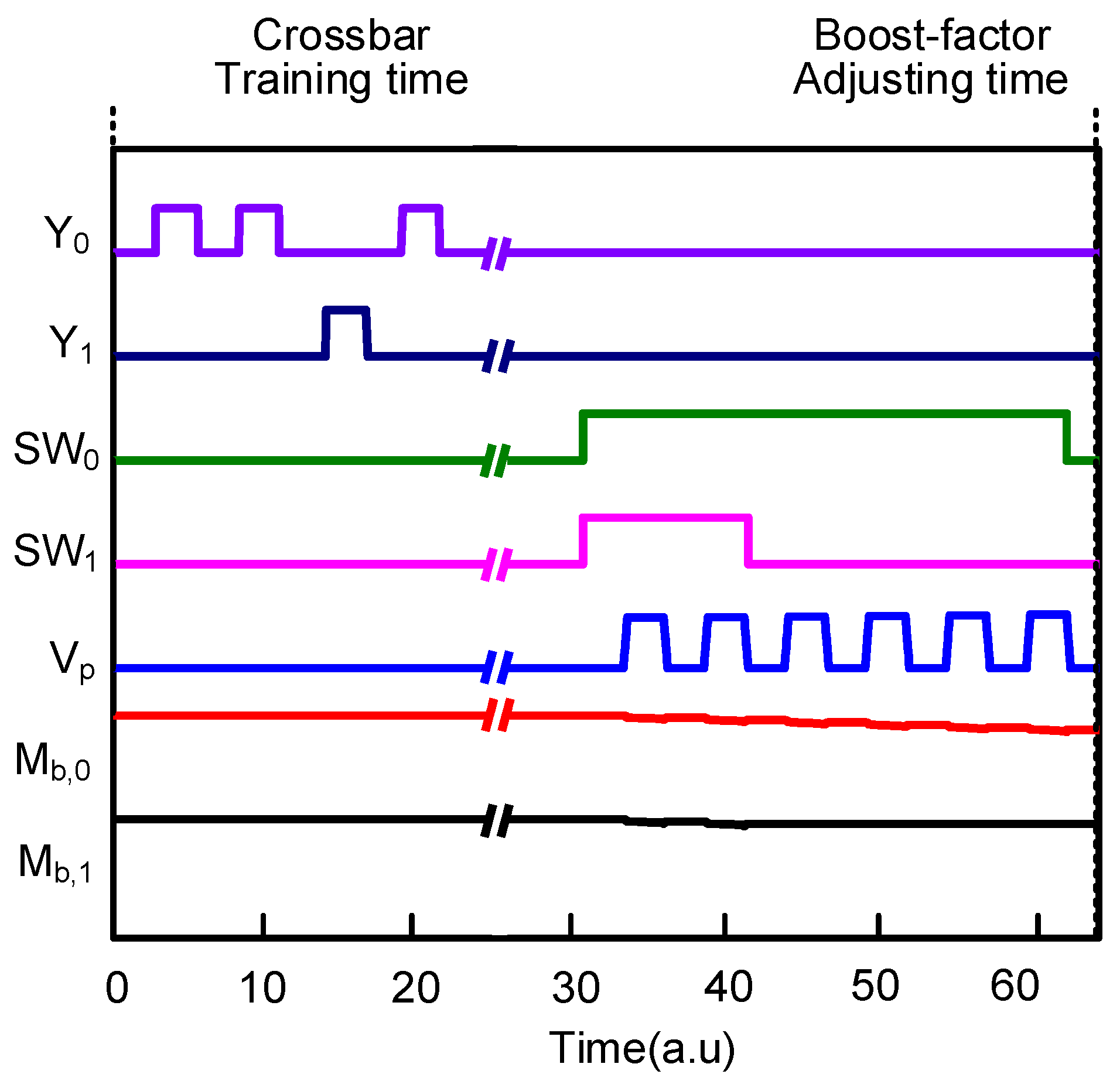
The simulated waveforms in
Figure 7 demonstrate the operation of the proposed memristor-CMOS hybrid circuit with the boost-factor adjustment. Here, the circuit simulation was performed using CADENCE SPECTRE (Cadence Design Systems, Inc., San Jose, CA, USA) and SAMSUNG 0.13-µm circuit simulation parameters [
25]. The mathematical equations of the Verilog-A model of memristors used in the circuit simulation were explained in-detail in a previous publication [
23]. In the simulation, we assumed the memristor crossbar of SP with 400 rows and 256 columns. The number of synaptic memristors per column is 25 among 400 cells. It means the 25 cells can be activated at the maximum among 400 cells per column in the crossbar. The increment and decrement of permanence are +0.01 and −0.01, respectively. The initial permanence values are assumed to be random between 0 and 1. The minimum amount of overlap between the input-space and spatial-pooler space can start from zero. The amount of overlap can be calculated by multiplying the input voltages with the memristor synaptic weights. The size of inhibition circuit zone is 64 columns in the crossbar. The number of winning columns is allowed not to exceed 2 among 64 columns. Thereby, the sparsity in
Figure 6a can be controlled within 2%, as the brain’s neocortex does.
In
Figure 7, during the crossbar training time, each column’s activity ratio is calculated by counting the number of activation of each column. If column #0 becomes activated, Y
0 becomes high. Similarly, if column #1 becomes activated, Y
1 is high. After the crossbar training time, the boost factor can be adjusted according to each column’s activity ratio, as described in Equation (1). The more frequent activation of column #0 leads to decrease the boost factor more. The less frequent activation of column #1 reduces the boost factor little, as shown in
Figure 7. For adjusting the boost factors of columns #0 and #1, the pulse widths of SW
0 and SW
1, respectively, are modulated. M
b,0 can be decreased more than M
b,1 by many programming pulses of V
P, because SW
0 is high for a longer time than SW
1. On the contrary, M
b,1 is changed little, due to the fact that SW
1 is high only for a very short time. The pulse modulation of SW
0 and SW
1 can be controlled very easily by counting the number of activations of each column during the crossbar training time.
3. Simulation Results
For calculating the recognition rate, we tested MNIST vectors [
26,
27] with the proposed memristor-CMOS hybrid circuit. To reflect the real crossbar with non-ideal effects, we considered source resistance, neuron resistance, wire resistance, etc., in the recognition-rate simulation [
22].
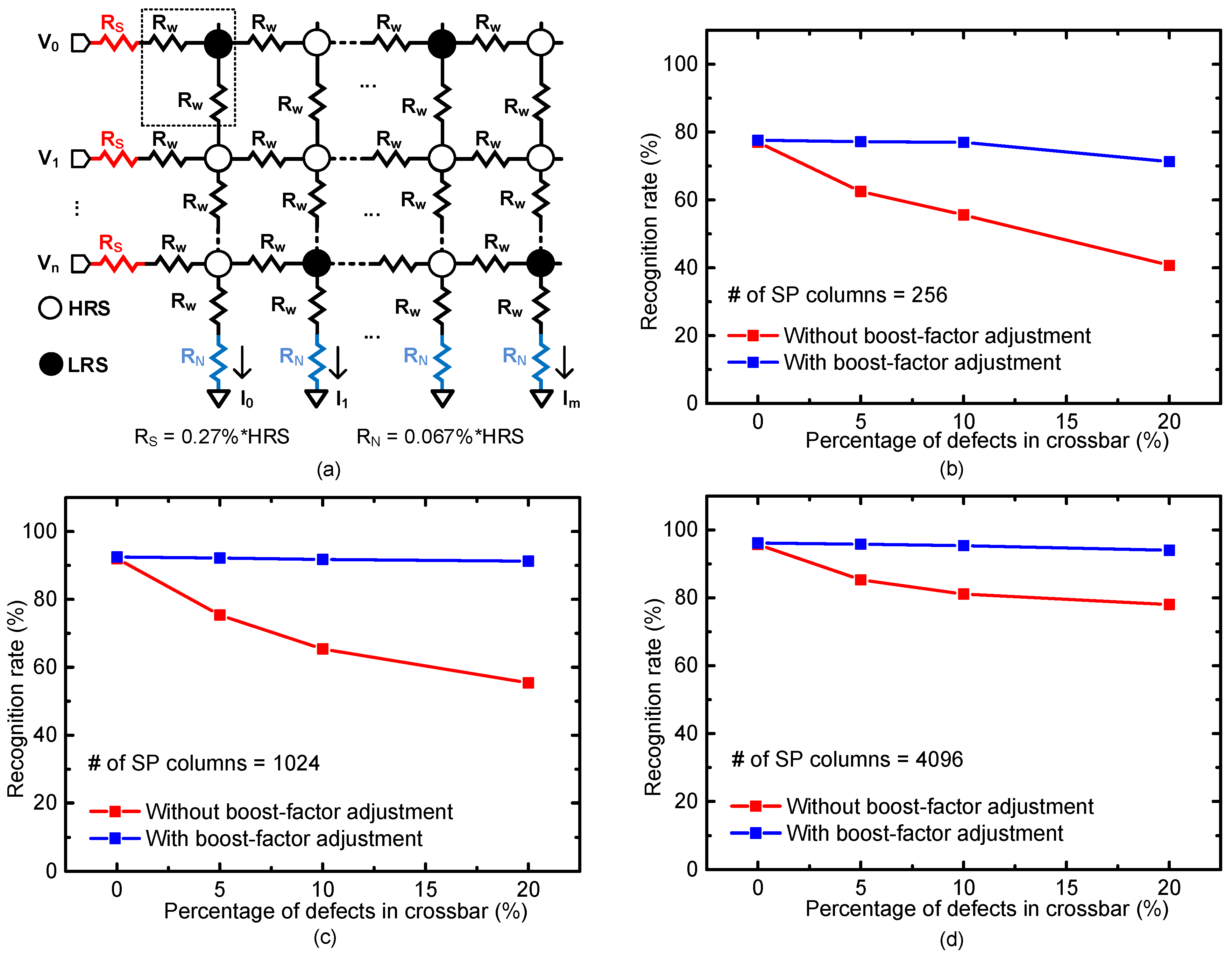
Figure 8a shows a schematic of memristor crossbar that includes these non-ideal parasitic effects. Here, R
S and R
N represent source resistance and neuron resistance, respectively [
2]. R
W represents wire resistance from metal layers. In the non-ideal crossbar, R
N and R
S are assumed to be 0.27% of HRS and 0.067% of HRS, respectively [
22]. R
W is assumed to be ~1Ω per cell in this paper. These R
S and R
N, which are 0.27% of HRS and 0.067% of HRS, respectively, are the worst-case values of the source and neuron resistance observed from the fabricated real crossbars [
22]. In
Figure 8a, V
0, V
1, and V
n represent the input voltages. I
0, I
1, and I
m represent the column currents.
We now explain the crossbar architecture for recognizing the MNIST vectors. Here, the number of rows in the crossbar should be 400, which should be the same with the number of input voltages. Each MNIST vector is composed of 20 × 20 = 400 pixels. Thus, the number of input voltages is 400 for recognizing the MNIST vector. For the number of columns of the SP crossbar, 256, 1024, and 4096 columns are used in
Figure 8b, c, and d, respectively. It is known that having more SP columns can result in a better recognition rate [
12]. This is because each SP column can store a specific feature of tested vectors. If the number of SP columns becomes larger, then more features can be stored in the columns. Thereby, the recognition rate for the tested images can be improved with increasing the number of SP columns. The number of SP columns = 256 is the same condition for the memristor-implemented Convolutional Neural Network, where the testing image has 20 × 20 pixels, the kernel size is 5 × 5, and the number of kernels = 1. Similarly, the number of SP columns = 1024 is the same condition of Convolutional Neural Network, with 20 × 20 image, 5 × 5 kernel, and the number of kernels = 4. The number of SP columns = 4096 is the same condition of Convolutional Neural Network, with 20 × 20 image, 5 × 5 kernel, and the number of kernels = 16. In this simulation, we did not simulate the crossbars with SP columns more than 4096, because we do not use the number of kernels more than 16 for recognizing the MNSIT vectors, in Convolutional Neural Network.
Figure 8b shows MNIST recognition rate of the memristor crossbar with SP columns = 256. Here, the percentage of defects in the crossbar is changed from 0% to 20%. The percentage σ of memristance variation of HRS and LRS is assumed to be zero. For the percentage of defects = 0%, the crossbars without and with the boost-factor adjustment show the recognition rates of 77.3% and 77.6%, respectively. When the percentage of defects is very small, the boost-factor adjustment affects the recognition rate very little. However, if the percentage increases, the boost-factor adjustment plays an important role to keep the recognition rate as high as the rate of defects = 0%, as shown in
Figure 8b. For the defects = 20%, the boost-factor adjustment can show the recognition rate better by as much as 30.6%, compared to the crossbar without the boost-factor adjustment.
Figure 8c is for the SP columns = 1024. As mentioned earlier, the crossbar with the SP columns = 1024 recognizes MNIST vectors better than the SP columns = 256. For the percentage of defects = 0%, the recognition rates of 256 and 1024 SP columns are 77.6% and 92.5%, respectively. As indicated in
Figure 8b, the boost-factor adjustment in
Figure 8c can maintain this good recognition rate, even though the percentage of defects is increased to 20%. For the percentage = 20%, the gap of recognition rates without and with the boost-factor adjustment is as much as 35.9%.
Figure 8d is for the SP columns = 4096. If the percentage of defects is 0%, the recognition rate of the crossbar is as high as 96.2%. In spite of the percentage of defects = 20%, the boost-factor adjustment can keep the rate as high as 94%, whereas the crossbar without the boost-factor adjustment is as low as 78%.
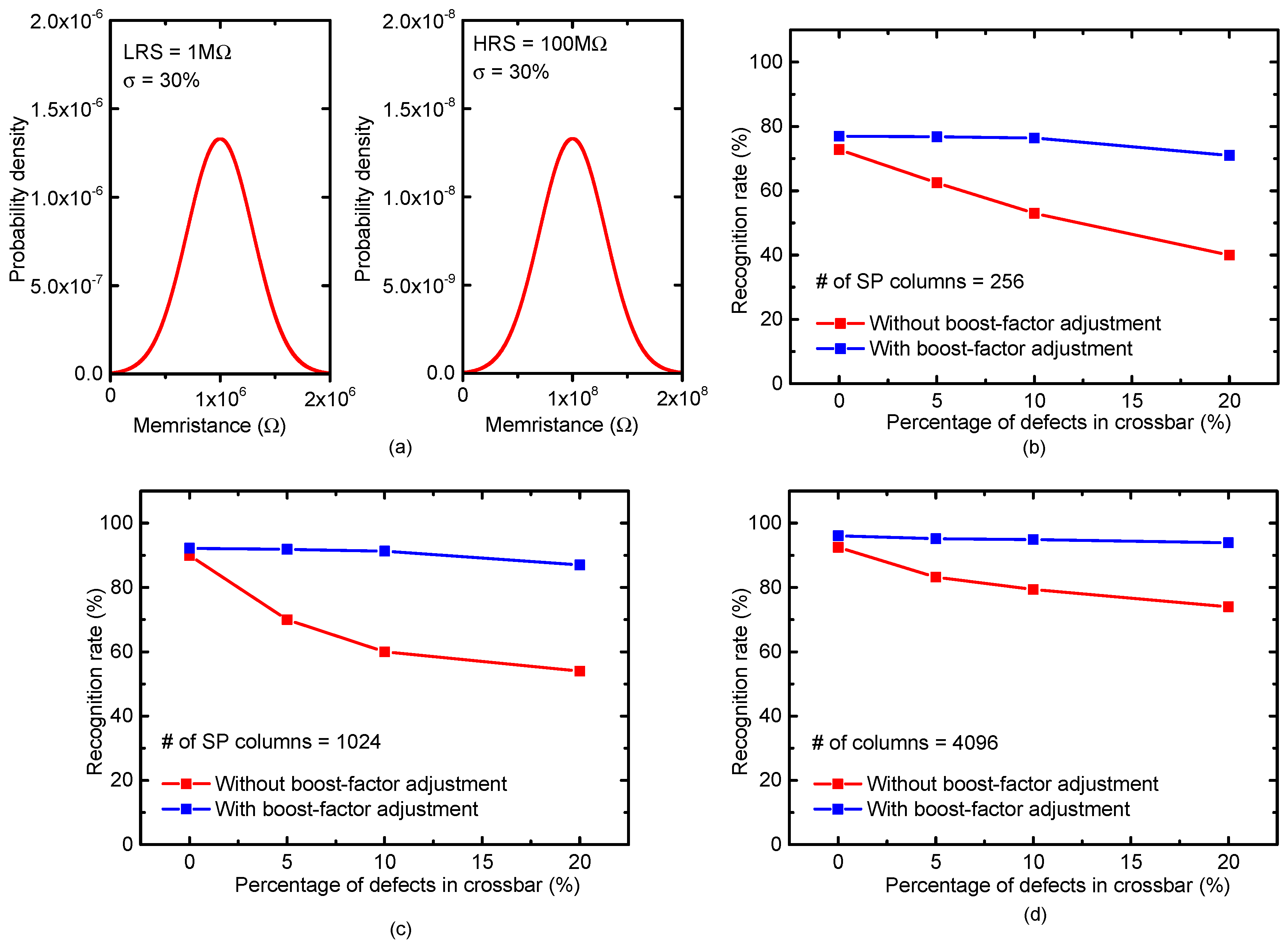
Figure 9a shows the statistical distributions of HRS and LRS, where the percentage σ of memristance variation is assumed to be 30%.
Figure 9 b, c, and d are for the SP columns = 256, 1024, and 4096, respectively. As indicated in
Figure 9, the more SP columns can result in the better recognition rate. In
Figure 9b, the percentage of defects is changed from 0% to 20%. For the percentage of defects = 0%, the boost-factor adjustment affects the recognition rate very little. However, if the percentage of defects is increased to 20%, the boost-factor adjustment can improve the recognition rate significantly compared to the crossbar without the boost-factor adjustment. Similarly, in
Figure 9c with the SP columns = 1024, the recognition rates without and with the boost-factor adjustment are 54% and 87%, respectively, when the defects = 20%. In
Figure 9d with the SP columns = 4096, the recognition rates without and with the boost-factor adjustment are 74% and 93.9%, respectively, when the defects = 20%.
4. Discussion
In this session, to understand the benefit of the proposed circuit exactly, we discuss and compare the following three SP schemes in
Table 1: (1) Spatial-pooling without both the boost-factor adjustment and the defect-aware mapping, (2) spatial-pooling with the defect-aware mapping, and (3) spatial-pooling with the boost-factor adjustment.
First, we discuss the possibility of hardware implementation in
Table 1. As mentioned earlier, (1) and (3) can be implemented in hardware. However, the defect-aware mapping of (2), as indicated in
Figure 2d, demands very complicated circuits such as memory, processor, controller, etc.
Second, the energy consumptions of the crossbar programming are compared among (1), (2), and (3) in
Table 1. The amount of programming energy is simulated during the training time of 10,000 MNIST vectors (1) and (2) consume 3.9 mJ for programming the crossbar with HRS and LRS, according to Hebbian learning rule, as explained in
Figure 4a. The energy overhead due to the boost-factor adjustment is less than ~0.05% of the crossbar programming energy. This is because each column has only one memristor for the boost-factor adjustment, compared to 400 cells per column for Hebbian learning.
For the recognition rate, in
Table 1 (1), without the boost-factor adjustment and defect-aware mapping, shows MNIST recognition rates of 77.3% and 55.6%, when the defects = 0% and 10%, respectively. Similarly, (2), with only the defect-aware mapping, shows the rates of 77.3% and 56.3%, when the defects = 0% and 10%, respectively. Without the boost-factor adjustment, the defective columns necessarily become activated frequently. The frequent activation of defective columns degrades the recognition rate significantly, as shown in (2) in
Table 1. On the contrary, (3) with the boost-factor adjustment shows the rates of 77.6% and 77%, when the defects = 0% and 10%, respectively. It has very little loss of the recognition rate, in spite of the defects = 10%. The gap between the defects = 0% and 10% is negligibly small for the crossbar with the boost-factor adjustment.
We now discuss the relationship of this work to the previous works performed in HTM hardware realization. Actually, as a previous works of this paper, we developed the memristor crossbar circuits for performing the SP and TM operations of HTM, respectively [
12,
13]. However, in the previous works, we did not consider the memristor defects, which should be taken into account in the real memristor crossbar having defects of stuck-at-faults and variations. Thus, the SP hardware implemented with the real defective memristor crossbar can be an essential part of future HTM’s hardware system. Additionally, as a further work, we try to fabricate the crossbar having more than 100 memristors and combine the fabricated crossbar with the CMOS circuit to verify the SP operation by hardware, for testing the MNSIT vectors.
Finally, we discuss possible applications of the memristor-CMOS hybrid circuit of HTM’s hardware. As Internet of Things (IoT) sensors become more popular in human life and environment, an amount of data generated from the sensors becomes enormous [
28,
29,
30]. To handle this huge amount of data from the physical world, we can think of the integration of IoT sensors and memristor-CMOS hybrid circuit into one chip [
31,
32]. By doing so, the unstructured data from the sensors can be pre-processed and interpreted near the sensors by the integrated memristor-CMOS hybrid circuit of HTM hardware. If we deliver all the data generated from the IoT sensors to the cloud, without any pre-processing of the unstructured data near the IoT sensors, an amount of computing energy demanded at the cloud may be huge [
33]. Thus, the memristor-CMOS hybrid circuit that can perform the pre-processing of the unstructured data from the IoT sensors can be very useful for energy-efficient computing in future.


