Growth of U-Shaped Graphene Domains on Copper Foil by Chemical Vapor Deposition


 and
and 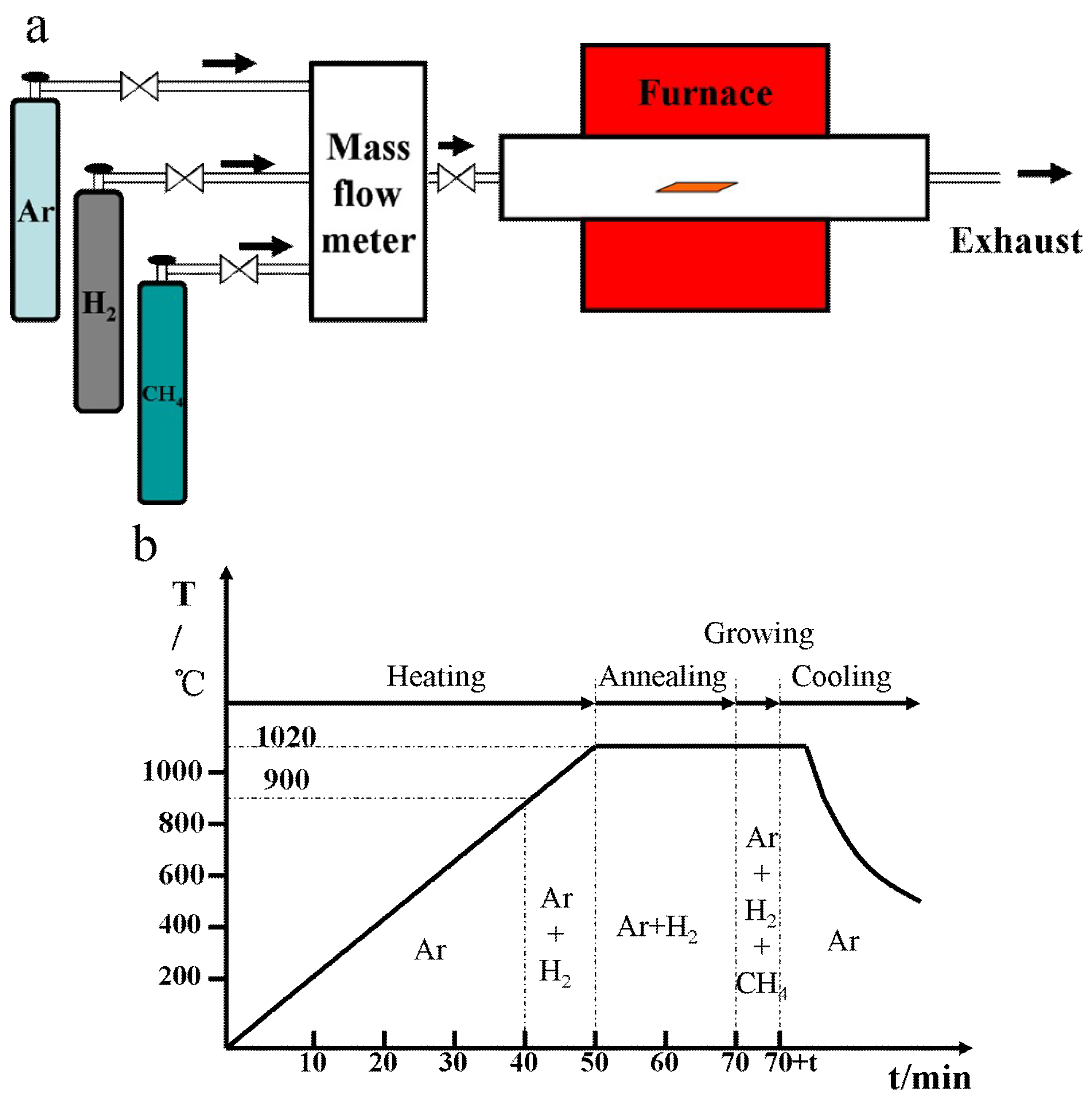
Abstract
1. Introduction
2. Experimental Section
2.1. Synthesis of Graphene Domains by CVD
2.2. Transfer of Graphene
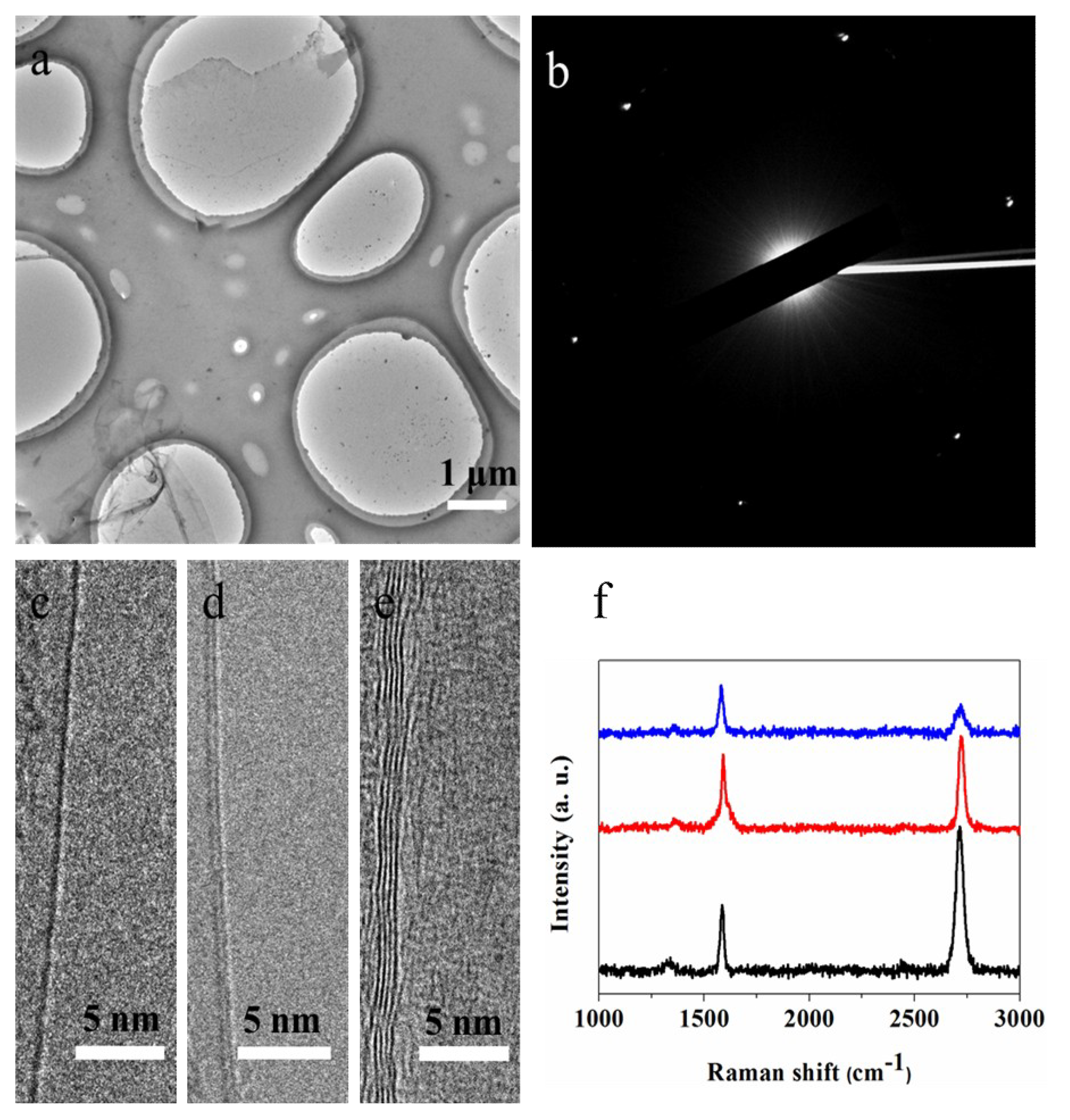
2.3. Graphene Characterization
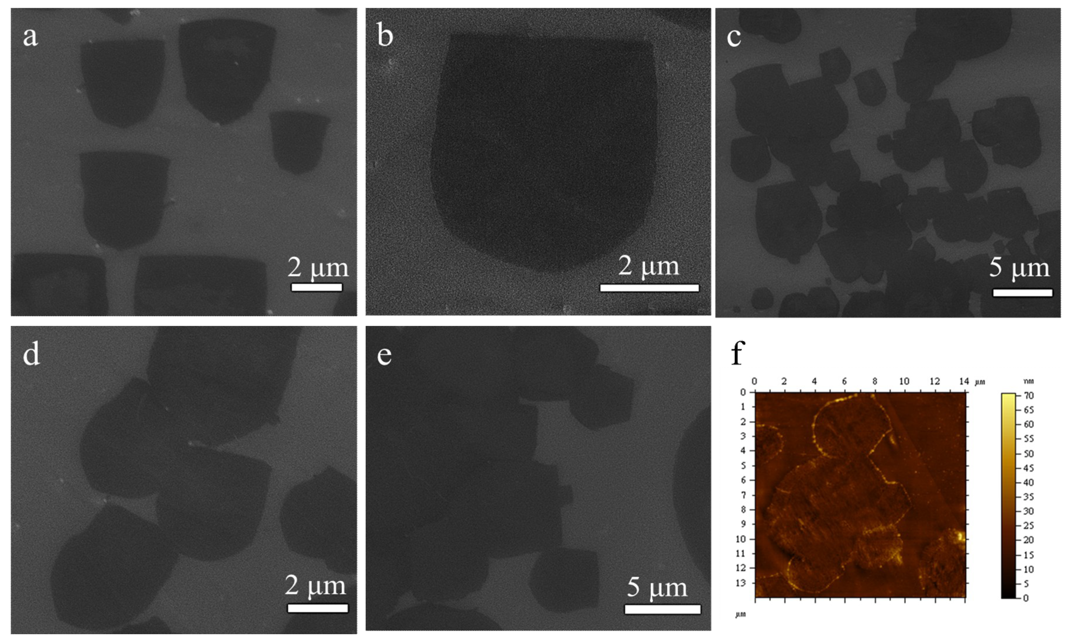
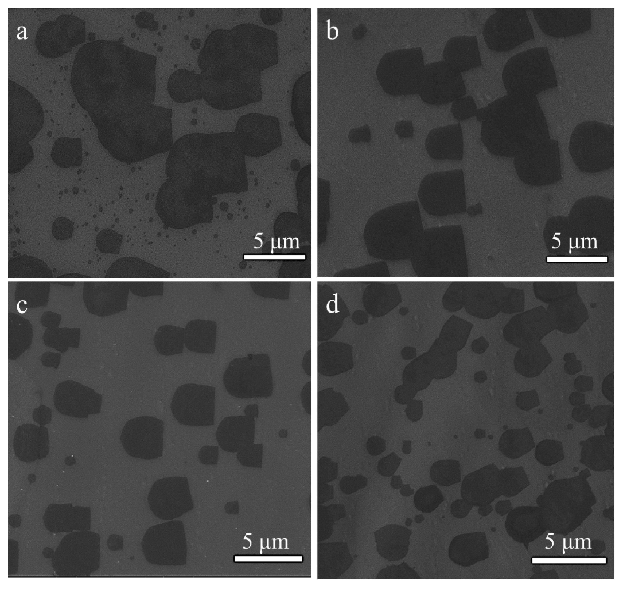
3. Results and Discussion
4. Conclusions
Author Contributions
Funding
Acknowledgments
Conflicts of Interest
References
- Huang, P.Y.; Ruiz-Vargas, C.S.; Van der Zande, A.M.; Whitney, W.S.; Levendorf, M.P.; Kevek, J.W.; Garg, S.; Alden, J.S.; Hustedt, C.J.; Zhu, Y.; et al. Grains and grain boundaries in single-layer graphene atomic patchwork quilts. Nature 2011, 463, 389–392. [Google Scholar] [CrossRef] [PubMed]
- Lee, C.; Wei, X.D.; Kysar, J.W.; Hone, J. Measurement of the elastic properties and intrinsic strength of monolayer graphene. Science 2008, 321, 385–388. [Google Scholar] [CrossRef] [PubMed]
- Bagri, A.; Kim, S.P.; Ruoff, R.S.; Shenoy, V.B. Thermal transport across twin grain boundaries in polycrystalline graphene from nonequilibrium molecular dynamics simulations. Nano Lett. 2011, 11, 3917–3921. [Google Scholar] [CrossRef] [PubMed]
- Novoselov, K.S.; Geim, A.K.; Morozov, S.V.; Jiang, D.; Zhang, Y.; Dubonos, S.V.; Grigorieva, I.V.; Firsov, A.A. Electric field effect in atomically thin carbon films. Science 2004, 306, 666–669. [Google Scholar] [CrossRef] [PubMed]
- Schniepp, H.C.; Li, J.L.; McAllister, M.J.; Sai, H.; Herrera-Alonso, M.; Adamson, D.H.; Prud’homme, P.K.; Car, R.; Saville, D.A.; Aksay, I.A. Functionalized single graphene sheets derived from splitting graphite oxide. J. Phys. Chem. B 2006, 110, 8535–8539. [Google Scholar] [CrossRef] [PubMed]
- Eda, G.; Fanchini, G.; Chhowalla, M. Large-area ultrathin films of reduced graphene oxide as a transparent and flexible electronic material. Nat. Nanotechnol. 2008, 3, 270–274. [Google Scholar] [CrossRef]
- Yan, Z.; Lin, J.; Peng, Z.W.; Sun, Z.Z.; Li, L.; Xiang, C.S.; Samuel, E.L.; Kittrell, C.; Tour, J.M. Toward the synthesis of wafer-scale single-crystal graphene on copper foils. ACS Nano 2013, 7, 2872. [Google Scholar] [CrossRef]
- Berger, C.; Song, Z.M.; Li, T.B.; Ogbazghi, A.Y.; Feng, R.; Dai, Z.T.; Marchenkov, A.N.; Conrad, E.H.; First, P.N.; et al. Ultrathin epitaxial graphite: 2D electron gas properties and a route toward graphene-based nanoelectronics. J. Phys. Chem. B 2004, 108, 19912–19916. [Google Scholar] [CrossRef]
- Li, X.S.; Cai, W.W.; An, J.H.; Kim, S.; Nah, J.; Yang, D.X.; Piner, R.; Velamakanni, A.; Jung, I.; Tutuc, E.; et al. Large-area synthesis of high-quality and uniform graphene films on copper foils. Science 2009, 324, 1312–1314. [Google Scholar] [CrossRef]
- Reina, A.; Jia, X.T.; Ho, J.; Nezich, D.; Son, H.B.; Bulovic, V.; Dresselhaus, M.S.; Kong, J. Large area, few-layer graphene films on arbitrary substrates by chemical vapor deposition. Nano Lett. 2009, 9, 30–35. [Google Scholar] [CrossRef]
- Li, X.S.; Cai, W.W.; Colombo, L.; Ruoff, R.S. Evolution of graphene growth on Ni and Cu by carbon isotope labeling. Nano Lett. 2009, 9, 4268–4272. [Google Scholar] [CrossRef]
- Yu, Q.K.; Lian, J.; Siriponglert, S.; Li, H.; Chen, Y.P.; Pei, S.S. Graphene segregated on Ni surfaces and transferred to insulators. Appl. Phys. Lett. 2008, 93, 113103. [Google Scholar] [CrossRef]
- Grantab, R.; Shenoy, V.B.; Ruoff, R.S. Anomalous strength characteristics of tilt grain boundaries in graphene. Science 2010, 330, 946–948. [Google Scholar] [CrossRef] [PubMed]
- Yu, Q.K.; Jauregui, L.A.; Wu, W.; Colby, R.; Tian, J.F.; Su, Z.H.; Cao, H.L.; Liu, Z.H.; Pandey, D.; Wei, D.; et al. Control and characterization of individual grains and grain boundaries in graphene grown by chemical vapor deposition. Nat. Mater. 2011, 10, 443–449. [Google Scholar] [CrossRef]
- Robertson, A.W.; Warner, J.H. Hexagonal single crystal domains of few-layer graphene on copper foils. Nano Lett. 2011, 11, 1182–1189. [Google Scholar] [CrossRef]
- Wu, B.; Geng, D.C.; Guo, Y.L.; Huang, L.P.; Xue, Y.Z.; Zheng, J.; Chen, J.Y.; Yu, G.; Liu, Y.Q.; Jiang, L.; et al. Equiangular hexagon-shape-controlled synthesis of graphene on copper surface. Adv. Mater. 2011, 23, 3522. [Google Scholar] [CrossRef] [PubMed]
- Wu, B.; Geng, D.C.; Xu, Z.P.; Guo, Y.P.; Huang, L.P.; Xue, Y.Z.; Chen, J.Y.; Yu, G.; Liu, Y.Q. Self-organized graphene crystal patterns. NPG Asia Mater. 2013, 5, e36. [Google Scholar] [CrossRef]
- Vlassiouk, I.; Regmi, M.; Fulvio, P.F.; Dai, S.; Datskos, P.; Eres, G.; Smirnov, S. Role of hydrogen in chemical vapor deposition growth of large single-crystal graphene. ACS Nano 2011, 5, 6069–6076. [Google Scholar] [CrossRef] [PubMed]
- Geng, D.C.; Wu, B.; Guo, Y.L.; Huang, L.P.; Xue, Y.Z.; Chen, J.Y.; Yu, G.; Jiang, L.; Hu, W.P.; Liu, Y. Uniform hexagonal graphene flakes and films grown on liquid copper surface. Proc. Natl. Acad. Sci. USA 2012, 109, 7992–7996. [Google Scholar] [CrossRef] [PubMed]
- Zhou, H.L.; Yu, W.J.; Liu, L.X.; Cheng, R.; Chen, Y.; Huang, X.Q.; Liu, Y.; Wang, Y.; Huang, Y.; Duan, X. Chemical vapour deposition growth of large single crystals of monolayer and bilayer graphene. Nat. Commun. 2013, 4, 2096. [Google Scholar] [CrossRef] [PubMed]
- Wofford, J.M.; Nie, S.; McCarty, K.F.; Bartelt, N.; Dubon, O.D. Graphene islands on Cu foils: The interplay between shape, orientation, and defects. Nano Lett. 2010, 10, 4890–4896. [Google Scholar] [CrossRef]
- Li, X.S.; Magnuson, C.W.; Venugopal, A.; Venugopal, A.; An, J.H.; Suk, J.W.; Han, B.Y.; Borysiak, M.; Cai, W.W.; Velamakanni, A.; et al. Graphene films with large domain size by a two-step chemical vapor deposition process. Nano Lett. 2010, 10, 4328–4334. [Google Scholar] [CrossRef] [PubMed]
- Geng, D.C.; Gao, E.L.; Wang, H.P.; Xu, J.; Xu, Z.P.; Yu, G. Large-area growth of five-lobed and triangular graphene grains on textured Cu substrate. Adv. Mater. Interfaces 2016, 3, 1600347. [Google Scholar] [CrossRef]
- Liu, J.W.; Wu, J.; Edwards, C.M.; Berrie, C.L.; Moore, D.; Chen, Z.J.; Maroni, V.A.; Paranthaman, M.P.; Goyal, A. Triangular graphene grain growth on cube-textured Cu substrates. Adv. Funct. Mater. 2011, 21, 3868–3874. [Google Scholar] [CrossRef]
- Wu, Y.A.; Robertson, A.W.; Schaffel, F.; Speller, S.C.; Warner, J.H. Aligned rectangular few-layer graphene domains on copper surfaces. Chem. Mater. 2011, 23, 4543–4547. [Google Scholar] [CrossRef]
- Dai, G.P.; Wu, M.H.; Taylor, D.K.; Vinodgopal, K. Square-shaped, single-crystal, monolayer graphene domains by low-pressure chemical vapor deposition. Mater. Res. Lett. 2013, 1, 67–76. [Google Scholar] [CrossRef]
- Wang, H.; Wang, G.Z.; Bao, P.F.; Yang, S.L.; Zhu, W.; Xie, X.; Zhang, W.J. Controllable synthesis of submillimeter single-crystal monolayer graphene domains on copper foils by suppressing nucleation. J. Am. Chem. Soc. 2012, 134, 3627–3630. [Google Scholar] [CrossRef] [PubMed]
- Liu, W.; Li, H.; Xu, C.; Khatami, Y.; Banerjee, K. Synthesis of high-quality monolayer and bilayer graphene on copper using chemical vapor deposition. Carbon 2011, 49, 4122–4130. [Google Scholar] [CrossRef]
- Jung, D.H.; Kang, C.; Yoon, D.; Cheong, H.; Lee, J.S. Anisotropic behavior of hydrogen in the formation of pentagonal graphene domains. Carbon 2015, 89, 242–248. [Google Scholar] [CrossRef]
- Geng, D.C.; Meng, L.; Chen, B.Y.; Gao, E.L.; Yan, W.; Yan, H.; Luo, B.R.; Xu, J.; Wang, H.P.; Mao, Z.; et al. Controlled growth of single-crystal twelve-pointed graphene grains on a liquid Cu surface. Adv. Mater. 2014, 26, 6423–6429. [Google Scholar] [CrossRef]
- Nguyen, V.L.; Shin, B.G.; Duong, D.L.; Kim, S.T.; Perello, D.; Lim, Y.J.; Yuan, Q.H.; Ding, F.; Jeong, H.Y.; Shin, H.S.; et al. Seamless stitching of graphene domains on polished copper. Adv. Mater. 2015, 27, 1376–1382. [Google Scholar] [CrossRef] [PubMed]
- Xue, R.W.; Abidi, I.H.; Luo, Z.T. Domain size, layer number and morphology control for graphene grown by chemical vapor deposition. Funct. Mater. Lett. 2017, 10, 1730003. [Google Scholar] [CrossRef]
- Zhang, Z.Y.; Lagally, M.G. Atomistic processes in the early stages of thin-film growth. Science 1997, 276, 377–383. [Google Scholar] [CrossRef] [PubMed]


© 2019 by the authors. Licensee MDPI, Basel, Switzerland. This article is an open access article distributed under the terms and conditions of the Creative Commons Attribution (CC BY) license (http://creativecommons.org/licenses/by/4.0/).
Share and Cite
Pan, M.; Wang, C.; Li, H.-F.; Xie, N.; Wu, P.; Wang, X.-D.; Zeng, Z.; Deng, S.; Dai, G.-P. Growth of U-Shaped Graphene Domains on Copper Foil by Chemical Vapor Deposition. Materials 2019, 12, 1887. https://doi.org/10.3390/ma12121887
Pan M, Wang C, Li H-F, Xie N, Wu P, Wang X-D, Zeng Z, Deng S, Dai G-P. Growth of U-Shaped Graphene Domains on Copper Foil by Chemical Vapor Deposition. Materials. 2019; 12(12):1887. https://doi.org/10.3390/ma12121887
Chicago/Turabian StylePan, Ming, Chen Wang, Hua-Fei Li, Ning Xie, Ping Wu, Xiao-Di Wang, Zheling Zeng, Shuguang Deng, and Gui-Ping Dai. 2019. "Growth of U-Shaped Graphene Domains on Copper Foil by Chemical Vapor Deposition" Materials 12, no. 12: 1887. https://doi.org/10.3390/ma12121887
APA StylePan, M., Wang, C., Li, H.-F., Xie, N., Wu, P., Wang, X.-D., Zeng, Z., Deng, S., & Dai, G.-P. (2019). Growth of U-Shaped Graphene Domains on Copper Foil by Chemical Vapor Deposition. Materials, 12(12), 1887. https://doi.org/10.3390/ma12121887