Metamorphic Integration of GaInAsSb Material on GaAs Substrates for Light Emitting Device Applications


Abstract
1. Introduction
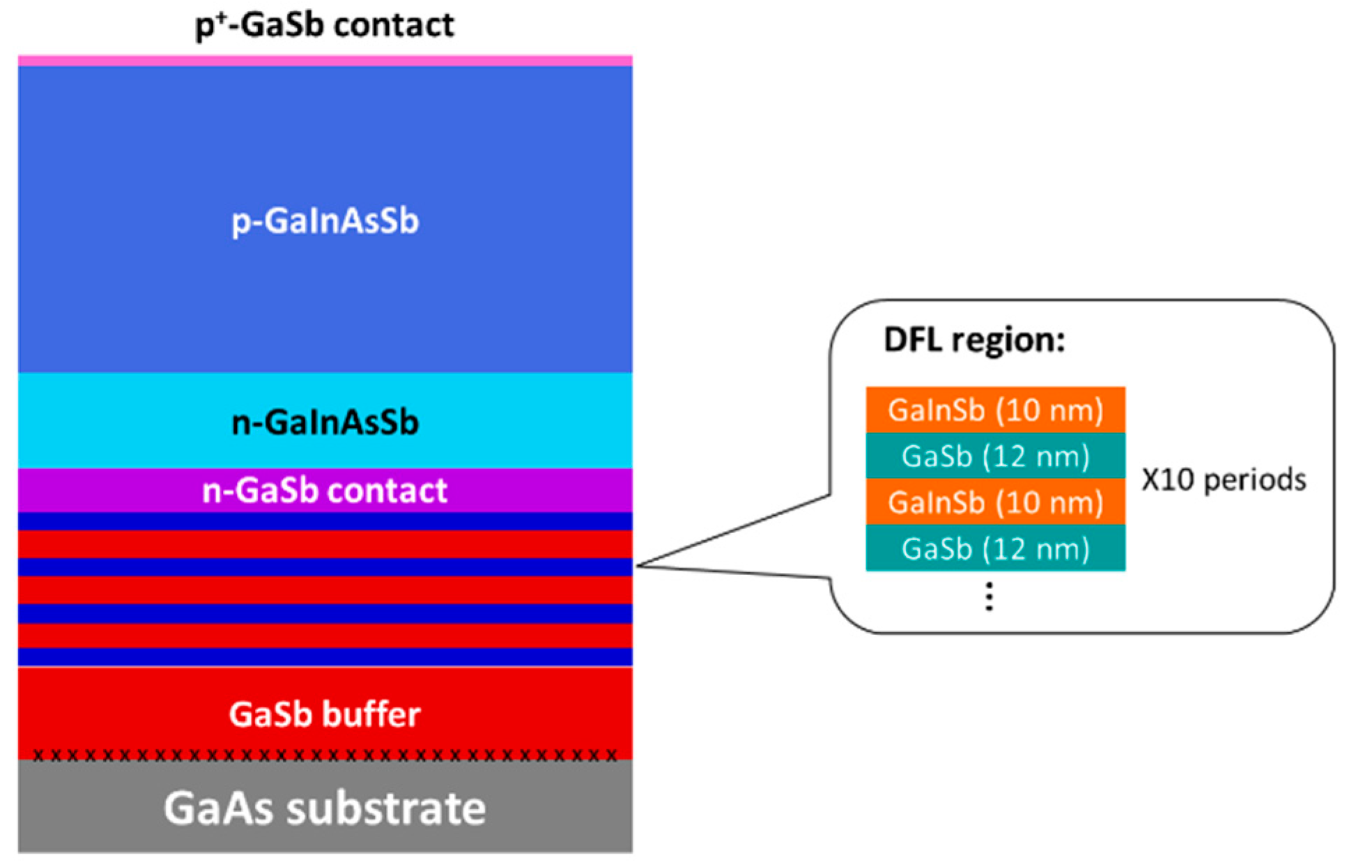
2. Experiments
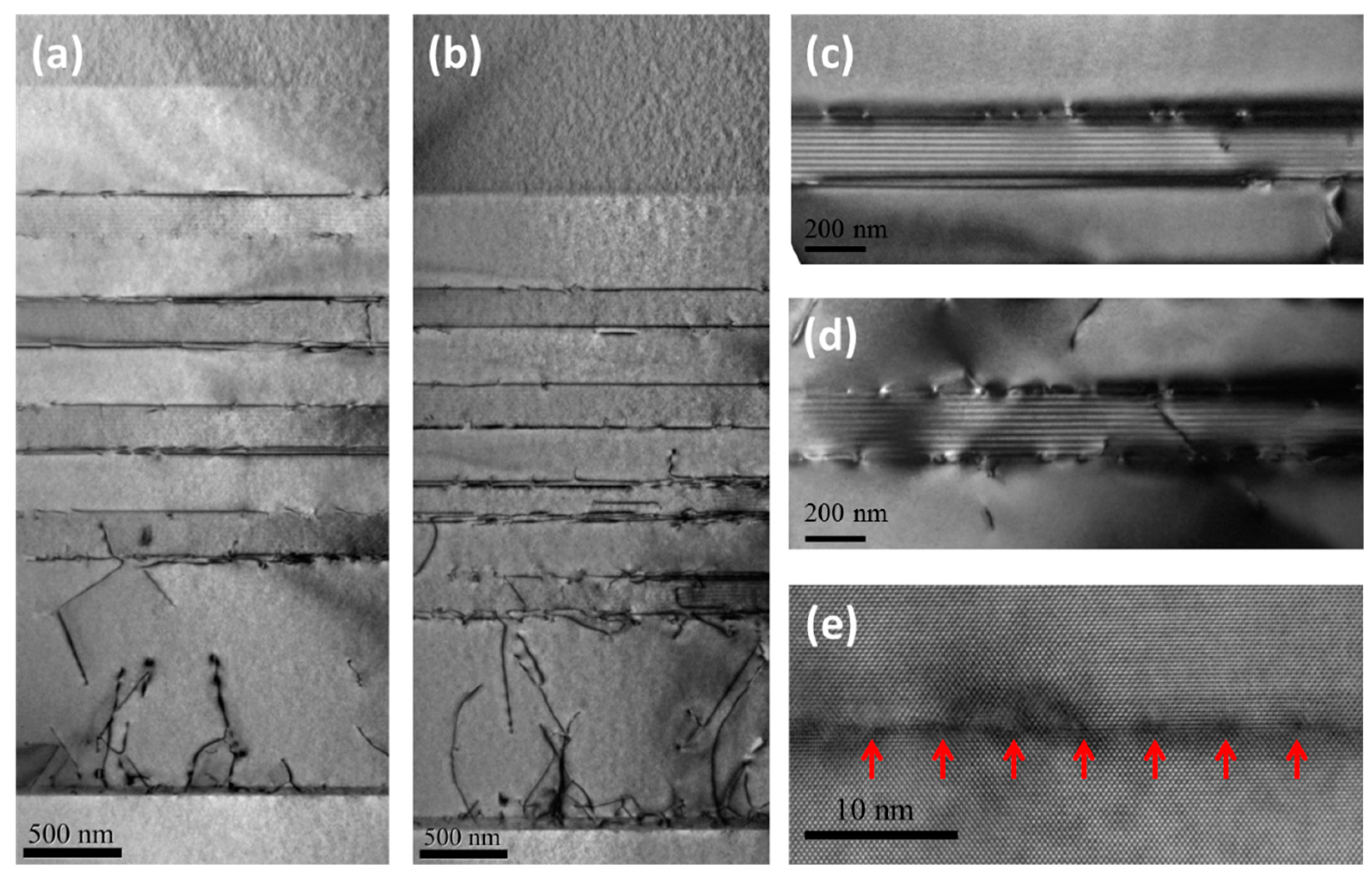
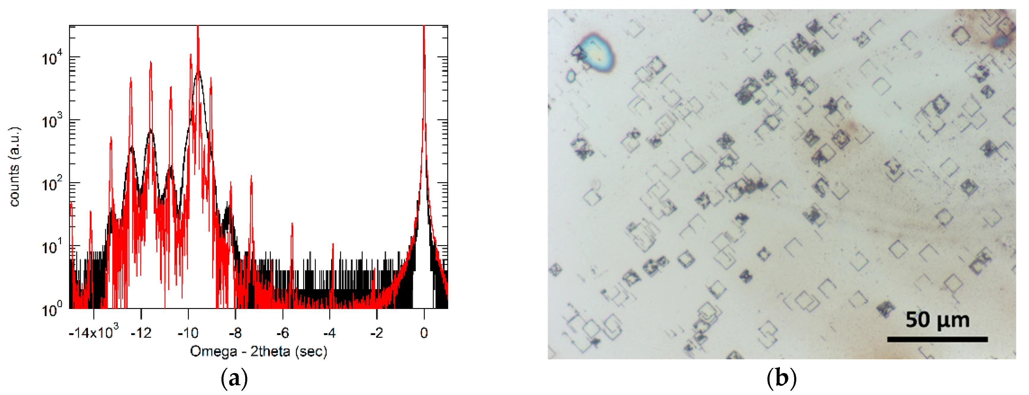
3. Results
3.1. Material Characterizations
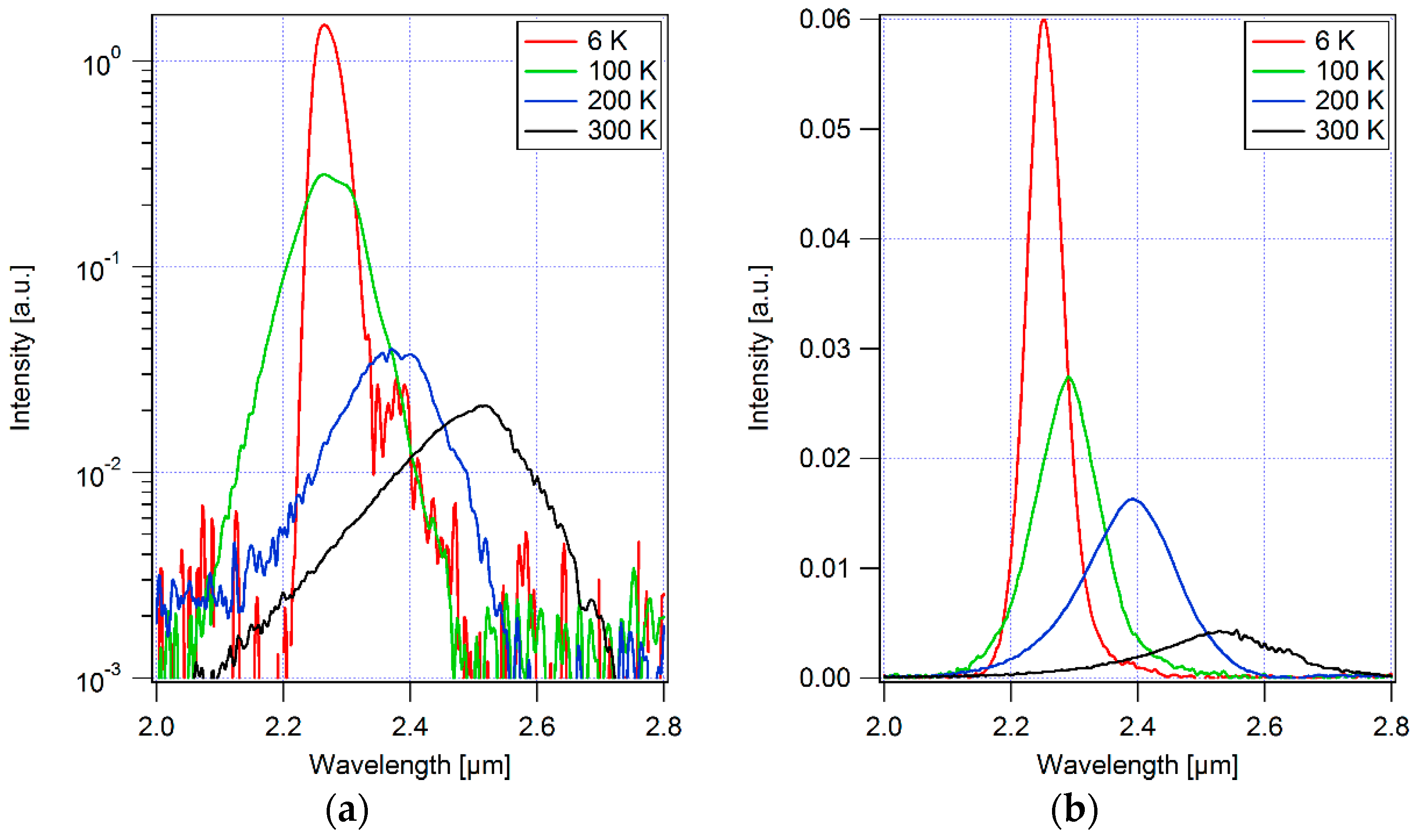
3.2. Photo-Luminescence and Electro-Luminescence
4. Discussion and Conclusions
Author Contributions
Funding
Acknowledgments
Conflicts of Interest
References
- Lei, L.; Li, L.; Lofti, H.; Jiang, Y.; Yang, R.Q.; Johnson, M.B.; Qiu, Y.; Lubyshev, D.; Fastenau, J.M.; Liu, A.W.K. Mid-wave interband cascade infrared photodetectors based on GaInAsSb absorbers. Semicond. Sci. Technol. 2016, 31, 105014. [Google Scholar] [CrossRef]
- Ikyo, A.B.; Marko, I.P.; Hild, K.; Adams, A.R.; Arafin, S.; Amann, M.C.; Sweeney, S.J. Temperature stable mid-infrared GaInAsSb/GaSb vertical cavity surface emitting lasers (VCSELs). Sci. Rep. 2016, 6, 19595. [Google Scholar] [CrossRef] [PubMed]
- Tang, L.; Xu, C.; Liu, Z.; Lu, Q.; Marshall, A.; Krier, A. Suppression of the surface “dead region” for fabrication of GaInAsSb thermophotovoltaic cells. Sol. Energy Mater. Sol. Cells. 2017, 163, 263–269. [Google Scholar] [CrossRef]
- Lin, C.; Grau, M.; Dier, O.; Amann, M.C. Low threshold room-temperature continuous-wave operation of 2.24–3.04 µm GaInAsSb/AlGaAsSb quantum-well lasers. Appl. Phys. Lett. 2004, 84, 5088–5090. [Google Scholar] [CrossRef]
- Lehnhardt, T.; Hümmer, M.; Rößner, K.; Müller, M.; Höfling, S.; Forchel, A. Continuous wave single mode operation of GaInAsSb/GaSb quantum well lasers emitting beyond 3 µm. Appl. Phys. Lett. 2008, 92, 183508. [Google Scholar] [CrossRef]
- Dashiell, M.W.; Beausang, J.F.; Ehsani, H.; Nichols, G.J.; Depoy, D.M.; Danielson, L.R.; Talamo, P.; Rahner, K.D.; Brown, E.J.; Burger, S.R.; et al. Quaternary InGaAsSb thermophotovoltaic diodes. IEEE Trans. Electron Devices 2006, 53, 2879–2888. [Google Scholar] [CrossRef]
- Liu, A.Y.; Herrick, R.W.; Ueda, O.; Petroff, P.M.; Gossard, A.C.; Bowers, J.E. Reliability of InAs/GaAs quantum dot lasers epitaxially grown on silicon. IEEE J. Sel. Top. Quantum Electron. 2015, 21, 1900708. [Google Scholar] [CrossRef]
- Karpov, S.Y.; Makarov, Y.N. Dislocation effect on light emission efficiency in gallium nitride. Appl. Phys. Lett. 2003, 81, 4721–4723. [Google Scholar] [CrossRef]
- France, R.M.; Geisz, J.F.; Steiner, M.A.; To, B.; Romero, M.J.; Olavarria, W.J.; King, R.R. Reduction of crosshatch roughness and threading dislocation density in metamorphic GaInP buffers and GaInAs solar cells. J. Appl. Phys. 2012, 111, 103528. [Google Scholar] [CrossRef]
- Chen, S.; Li, W.; Wu, J.; Jiang, Q.; Tang, M.; Shutts, S.; Elliott, S.N.; Sobiesierski, A.; Seeds, A.J.; Ross, I.; et al. Electrically pumped continuous-wave III-V quantum dot lasers on silicon. Nat. Photonics 2016, 10, 307–311. [Google Scholar] [CrossRef]
- Wang, Y.; Ruterana, P.; Desplanque, L.; El Kazzi, S.; Wallart, X. Strain relief at the GaSb/GaAs interface versus substrate surface treatment and AlSb interlayers thickness. J. Appl. Phys. 2011, 109, 23509. [Google Scholar] [CrossRef]
- Megalini, L.; Šuran Brunelli, S.T.; Charles, W.O.; Taylor, A.; Isaac, B.; Bowers, J.E.; Klamkin, J. Strain-compensated InGaAsP superlattices for defect reduction of InP Grown on exact-oriented (001) patterned Si substrates by metal organic chemical vapor deposition. Materials 2018, 11, 337. [Google Scholar] [CrossRef] [PubMed]
- Vurgaftman, I.; Meyer, J.R. Band parameters for III–V compound semiconductors and their alloys. J. Appl. Phys. 2001, 89, 5815. [Google Scholar] [CrossRef]
- Juang, B.C.; Laghumavarapu, R.B.; Foggo, B.J.; Simmonds, P.J.; Lin, A.; Liang, B.; Huffaker, D.L. GaSb thermophotovoltaic cells grown on GaAs by molecular beam epitaxy using interfacial misfit arrays. Appl. Phys. Lett. 2015, 106, 111101. [Google Scholar] [CrossRef]
- Huang, S.; Balakrishnan, G.; Huffaker, D.L. Interfacial misfit array formation for GaSb growth on GaAs. J. Appl. Phys. 2009, 105, 103104. [Google Scholar] [CrossRef]
- Hÿtch, M.J.; Snoeck, E.; Kilaas, R. Quantitative measurement of displacement and strain fields from HREM micrographs. Ultramicroscopy 1998, 74, 131–146. [Google Scholar] [CrossRef]
- Papis-Polakowska, E. Surface treatment of GaSb and related materials for the processing of mid-infrared semiconductor devices. Electron Technol. 2005/2006, 37/38, 1–34. [Google Scholar]
- Balakrishnan, G.; Huang, S.; Rotter, T.J.; Stintz, A.; Dawson, L.R.; Malloy, K.J.; Xu, H.; Huffaker, D.L. 2.0 μm wavelength InAs quantum dashes grown on a GaAs substrate using a metamorphic buffer layer. Appl. Phys. Lett. 2004, 84, 2058–2060. [Google Scholar] [CrossRef]
- Richardson, C.J.K.; He, L.; Apiratikul, P.; Siwak, N.P.; Leavitt, R.P. Improved GaSb-based quantum well laser performance through metamorphic growth on GaAs substrates. Appl. Phys. Lett. 2015, 106, 101108. [Google Scholar] [CrossRef]
- Megalini, L.; Cabinian, B.C.; Zhao, H.; Oakley, D.C.; Bowers, J.E.; Klamkin, J. Large-area direct hetero-epitaxial growth of 1550-nm InGaAsP multi-quantum-well structures on patterned exact-oriented (001) silicon substrates by metal organic chemical vapor deposition. J. Electron. Mater. 2018, 47, 982–987. [Google Scholar] [CrossRef]
- George, I.; Becagli, F.; Liu, H.Y.; Wu, J.; Tang, M.; Beanland, R. Dislocation filters in GaAs on Si. Semicond. Sci. Technol. 2015, 30, 114004. [Google Scholar] [CrossRef]
- Wan, Y.; Li, Q.; Liu, A.Y.; Gossard, A.C.; Bowers, J.E.; Hu, E.L.; Lau, K.M. Optically pumped 1.3 μm room-temperature InAs quantum-dot micro-disk lasers directly grown on (001) silicon. Opt. Lett. 2016, 41, 1664–1667. [Google Scholar] [CrossRef]
- Wu, J.; Jiang, Q.; Chen, S.; Tang, M.; Mazur, Y.I.; Maidaniuk, Y.; Benamara, M.; Semtsiv, M.P.; Masselink, W.T.; Sablon, K.A.; et al. Monolithically integrated InAs/GaAs quantum dot mid-infrared photodetectors on silicon substrates. ACS Photonics 2016, 3, 749–753. [Google Scholar] [CrossRef]
- Mehta, M.; Jallipalli, A.; Tatebayashi, J.; Kutty, M.N.; Albrecht, A.; Balakrishnan, G.; Dawson, L.R.; Huffaker, D.L. Room-temperature operation of buffer-free GaSb–AlGaSb quantum-well diode lasers grown on a GaAs platform emitting at 1.65 µm. IEEE Photonics Technol. Lett. 2007, 19, 1628–1630. [Google Scholar] [CrossRef]
- Mehta, M.; Balakrishnan, G.; Huang, S.; Khoshakhlagh, A.; Patel, P.; Kutty, M.N.; Dawson, L.R.; Huffaker, D.L. GaSb quantum-well-based “buffer-free” vertical LED monolithically embedded within a GaAs cavity using interfacial misfit arrays. Appl. Phys. Lett. 2007, 89, 211110. [Google Scholar] [CrossRef]
- Plis, E.; Rodriguez, J.B.; Balakrishnan, G.; Sharma, Y.D.; Kim, H.S.; Rotter, T.; Krishna, S. Mid-infrared InAs/GaSb strained layer superlattice detectors with nBn design grown on a GaAs substrate. Semicond. Sci. Technol. 2010, 25, 85010. [Google Scholar] [CrossRef]
- Ward, T.; Sánchez, A.M.; Tang, M.; Wu, J.; Liu, H.; Dunstan, D.J.; Beanland, R. Design rules for dislocation filters. J. Appl. Phys. 2014, 116, 63508. [Google Scholar] [CrossRef]


© 2019 by the authors. Licensee MDPI, Basel, Switzerland. This article is an open access article distributed under the terms and conditions of the Creative Commons Attribution (CC BY) license (http://creativecommons.org/licenses/by/4.0/).
Share and Cite
Lu, Q.; Marshall, A.; Krier, A. Metamorphic Integration of GaInAsSb Material on GaAs Substrates for Light Emitting Device Applications. Materials 2019, 12, 1743. https://doi.org/10.3390/ma12111743
Lu Q, Marshall A, Krier A. Metamorphic Integration of GaInAsSb Material on GaAs Substrates for Light Emitting Device Applications. Materials. 2019; 12(11):1743. https://doi.org/10.3390/ma12111743
Chicago/Turabian StyleLu, Qi, Andrew Marshall, and Anthony Krier. 2019. "Metamorphic Integration of GaInAsSb Material on GaAs Substrates for Light Emitting Device Applications" Materials 12, no. 11: 1743. https://doi.org/10.3390/ma12111743
APA StyleLu, Q., Marshall, A., & Krier, A. (2019). Metamorphic Integration of GaInAsSb Material on GaAs Substrates for Light Emitting Device Applications. Materials, 12(11), 1743. https://doi.org/10.3390/ma12111743