An Overview of Normally-Off GaN-Based High Electron Mobility Transistors


Abstract
:1. Introduction
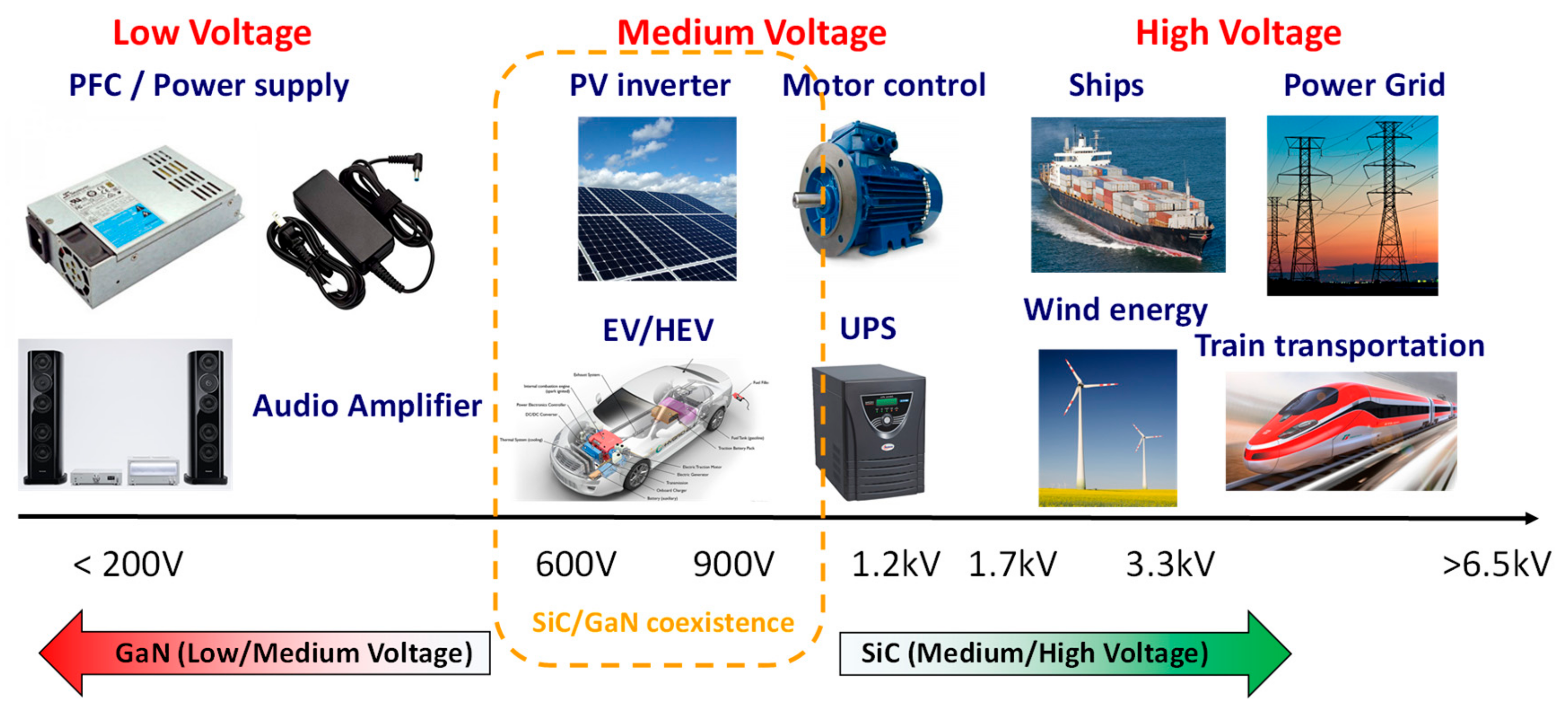
2. Gallium Nitride: Properties, Power Electronics Applications and Potential Market
3. Normally-Off GaN HEMT Technology
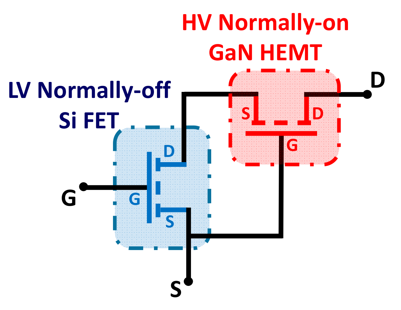
3.1. Cascode Configuration
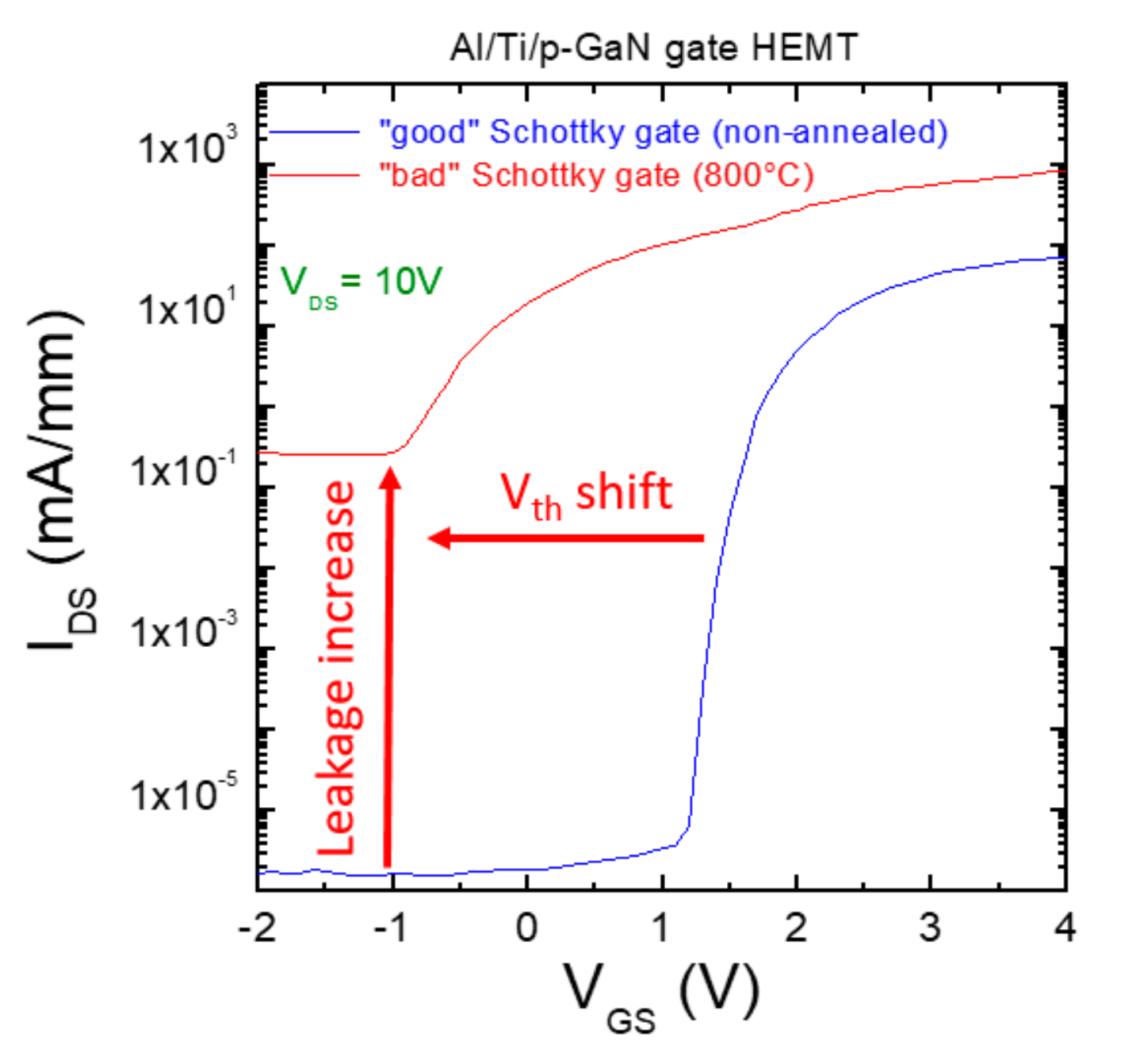
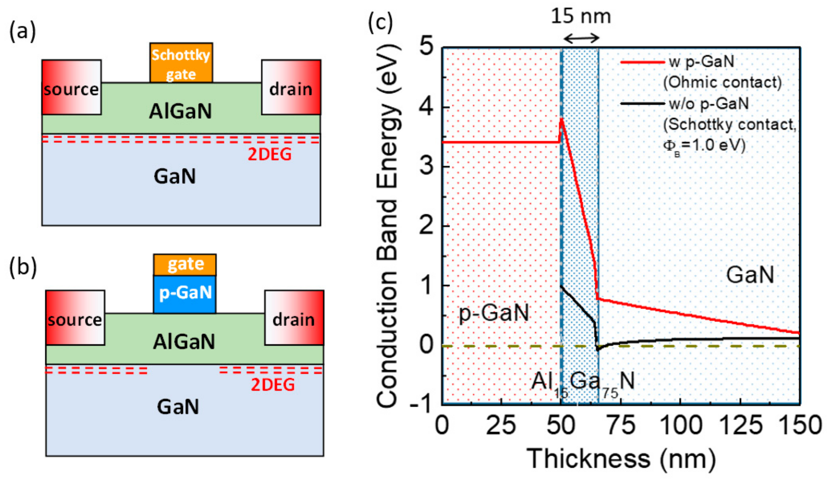
3.2. p-GaN Gate
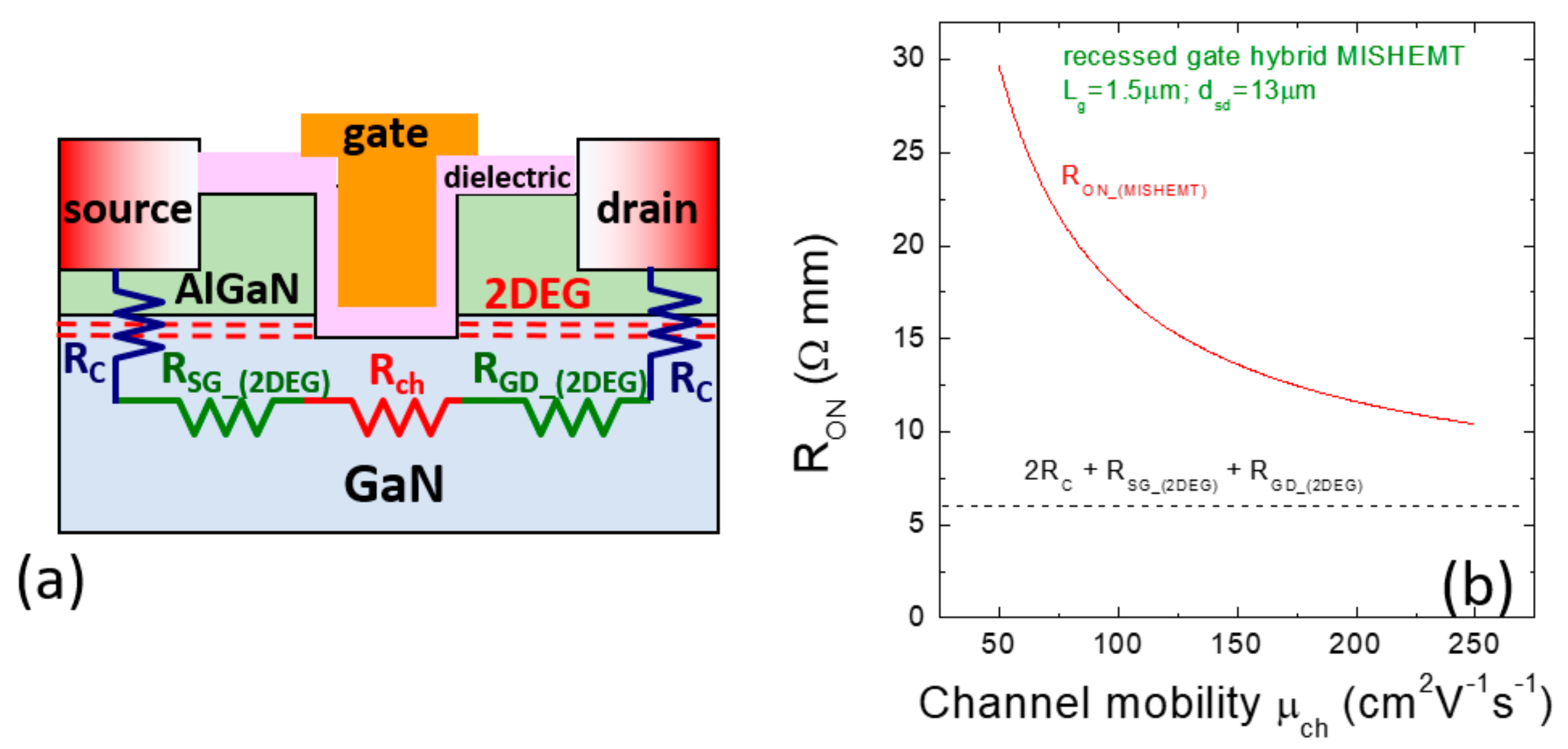
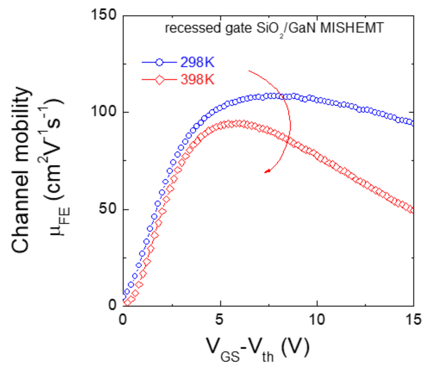
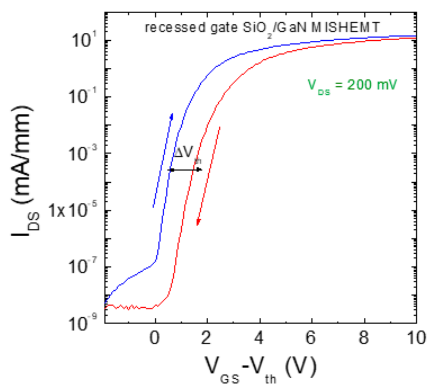
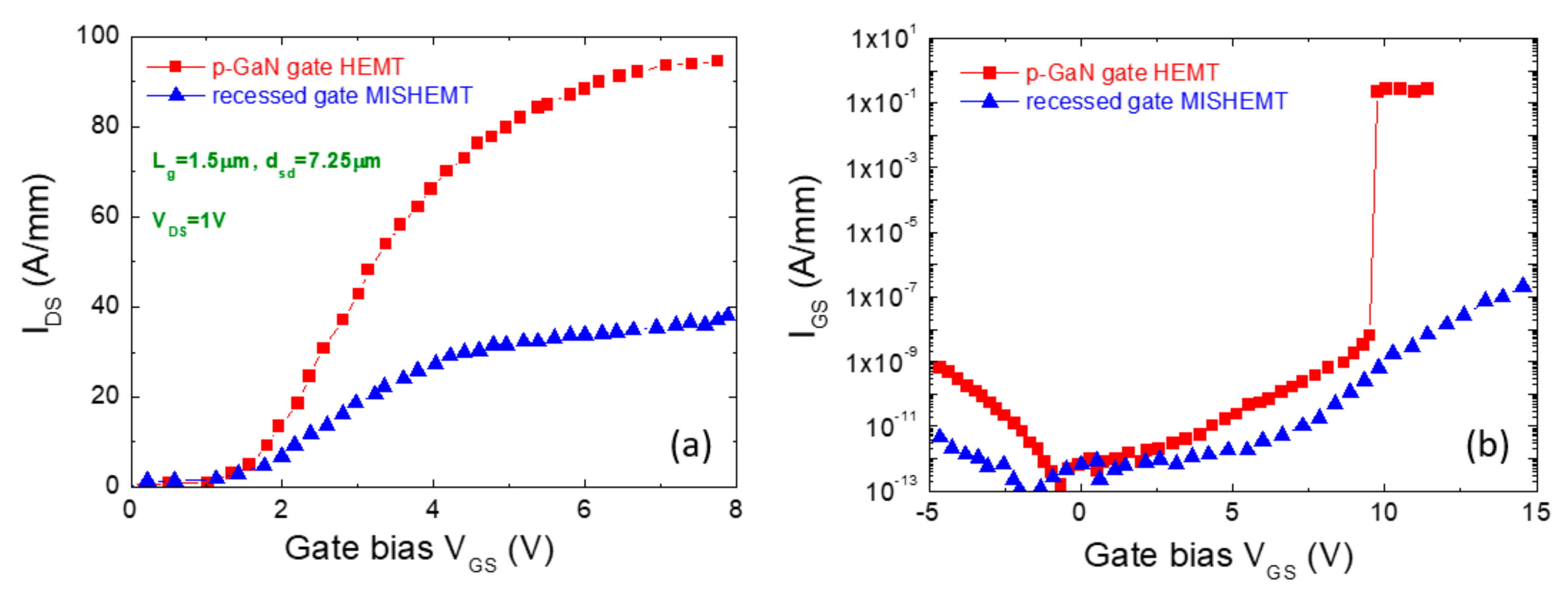
3.3. Recessed Gate Hybrid MISHEMT
4. Summary and Outlook
Author Contributions
Funding
Acknowledgments
Conflicts of Interest
References
- International Energy Agency (IEA). World Energy Outlook Report for 2016 (WEO-2016); IEA: Paris, France, 2016. [Google Scholar]
- Ren, F.; Zolper, J.C. Wide Band Gap Electronic Devices; World Scientific: Singapore, 2003. [Google Scholar]
- Kimoto, T.; Cooper, J.A. Fundamentals of Silicon Carbide Technology: Growth, Characterization, Devices and Applications; John Wiley & Sons Singapore Pte. Ltd.: Singapore, 2014. [Google Scholar]
- Roccaforte, F.; Fiorenza, P.; Greco, G.; Lo Nigro, R.; Giannazzo, F.; Patti, A.; Saggio, M. Challenges for energy efficient wide band gap semiconductor power devices. Phys. Status Solidi A 2014, 211, 2063–2071. [Google Scholar] [CrossRef]
- Ambacher, O.; Smart, J.; Shealy, J.R.; Weimann, N.G.; Chu, K.; Murphy, M.; Schaff, W.J.; Eastman, L.F.; Dimitrov, R.; Wittmer, L.; et al. Two-dimensional electron gases induced by spontaneous and piezoelectric polarization charges in N- and Ga-face AlGaN/GaN heterostructures. J. Appl. Phys. 1999, 85, 3222–3233. [Google Scholar] [CrossRef]
- Baliga, B.J. Power Semiconductor Device Figure of Merit for High-Frequency Applications. IEEE Electron Device Lett. 1989, 10, 455–457. [Google Scholar] [CrossRef]
- Roccaforte, F.; Giannazzo, F.; Iucolano, F.; Eriksson, J.; Weng, M.H.; Raineri, V. Surface and interface issues in wide band gap semiconductor electronics. Appl. Surf. Sci. 2010, 256, 5727–5735. [Google Scholar] [CrossRef]
- Shur, M.; Rumyanstev, S.; Levinshtein, M. SiC Materials and Devices; World Scientific: Singapore, 2006. [Google Scholar]
- Asif Khan, M.; Kuznia, J.N.; Bhattarai, A.R.; Olson, D.T. Metal semiconductor field effect transistor based on single crystal GaN. Appl. Phys. Lett. 1993, 62, 1786–1787. [Google Scholar] [CrossRef]
- Roccaforte, F.; Fiorenza, P.; Lo Nigro, R.; Giannazzo, F.; Greco, G. Physics and technology of gallium nitride materials for power electronics. Riv. Nuovo Cim. 2018, 41, 625–681. [Google Scholar]
- Villamor, A.; Zong, Z. Power GaN 2017: Epitaxy, Devices, Applications and Technology Trends 2017 Report; Yole Développement: Lyon, France, 2017. [Google Scholar]
- Chen, K.J.; Zhou, C. Enhancement-mode AlGaN/GaN HEMT and MIS-HEMT technology. Phys. Status Solidi A 2011, 208, 434–438. [Google Scholar] [CrossRef]
- Su, M.; Chen, C.; Rajan, S. Prospects for the application of GaN power devices in hybrid electric vehicle drive systems. Semicond. Sci. Technol. 2013, 28, 074012. [Google Scholar] [CrossRef]
- Scott, M.J.; Fu, L.; Zhang, X.; Li, J.; Yao, C.; Sievers, M.; Wang, J. Merits of gallium nitride based power conversion. Semicond. Sci. Technol. 2013, 28, 074013. [Google Scholar] [CrossRef]
- Saito, W.; Takada, Y.; Kuraguchi, M.; Tsuda, K.; Omura, I. Recessed-gate structure approach toward normally off high-Voltage AlGaN/GaN HEMT for power electronics applications. IEEE Electron Device Lett. 2006, 53, 356–362. [Google Scholar] [CrossRef]
- Kumar, V.; Kuliev, A.; Tanaka, T.; Otoki, Y.; Adesida, I. High transconductance enhancement-mode AlGaN/GaN HEMTs on SiC substrate. Electron. Lett. 2003, 39, 1758–1760. [Google Scholar] [CrossRef]
- Cai, Y.; Zhou, Y.; Lau, K.M.; Chen, K.J. Control of Threshold Voltage of AlGaN/GaN HEMTs by Fluoride-Based Plasma Treatment: From Depletion Mode to Enhancement Mode. IEEE Electron Device Lett. 2006, 53, 2207–2215. [Google Scholar] [CrossRef]
- Greco, G.; Giannazzo, F.; Frazzetto, A.; Raineri, V.; Roccaforte, F. Near-surface processing on AlGaN/GaN heterostructures: A nanoscale electrical and structural characterization. Nanoscale Res. Lett. 2011, 6, 132. [Google Scholar] [CrossRef] [PubMed]
- Zhang, Y.; Sun, M.; Joglekar, S.J.; Fujishima, T.; Palacios, T. Threshold voltage control by gate oxide thickness in fluorinated GaN metal-oxide semiconductor high-electron-mobility transistors. Appl. Phys. Lett. 2013, 103, 033524. [Google Scholar] [CrossRef]
- Lorenz, A.; Derluyn, J.; Das, J.; Cheng, K.; Degroote, S.; Medjdoub, F.; Germain, M.; Borghs, G. Influence of thermal anneal steps on the current collapse of fluorine treated enhancement mode SiN/AlGaN/GaN HEMTs. Phys. Status Solidi C 2009, 6, S996–S998. [Google Scholar] [CrossRef]
- Baliga, B.J. Silicon Carbide Power Devices; World Scientific Publising Co Pte. Ltd.: Singapore, 2005. [Google Scholar]
- Jones, E.A.; Wang, F.F.; Costinett, D. Review of commercial GaN power devices and GaN-based converter design challenges. IEEE J. Emerg. Sel. Top. Power Electron. 2016, 4, 707–719. [Google Scholar] [CrossRef]
- Lidow, A.; Strydom, J.; de Rooij, M.; Reutsch, D. GaN Transistors for Efficient Power Conversion; John Wiley & Sons Ltd.: Chichester, UK, 2015. [Google Scholar]
- Uemoto, Y.; Hikita, M.; Ueno, H.; Matsuo, H.; Ishida, H.; Yanagihara, M.; Ueda, T.; Tanaka, T.; Ueda, D. Gate Injection Transistor (GIT)—A Normally-Off AlGaN/GaN Power Transistor Using Conductivity Modulation. IEEE Trans. Electron Devices 2007, 54, 3393–3399. [Google Scholar] [CrossRef]
- Fujii, T.; Tsuyukuchi, N.; Hirose, Y.; Ywaya, M.; Kamiyama, S.; Amano, H.; Akasaki, I. Fabrication of enhancement-mode AlxGa1–xN/GaN junction heterostructure field-effect transistors with p-type GaN gate contact. Phys. Status Solidi C 2007, 4, 2708–2711. [Google Scholar] [CrossRef]
- Hilt, O.; Knauer, A.; Brunner, F.; Bahat-Treidel, E.; Würfl, J. Normally-off AlGaN/GaN HFET with p-type GaN Gate and AlGaN Buffer. In Proceedings of the 22nd International Symposium on Power Semiconductor Devices and IC’s (ISPSD2010), Hiroshima, Japan, 6–10 June 2010; pp. 347–350. [Google Scholar]
- Hilt, O.; Brunner, F.; Cho, E.; Knauer, A.; Bahat-Treidel, E.; Würfl, J. Normally-off High-Voltage p-GaN Gate GaN HFET with Carbon-Doped Buffer. In Proceedings of the 23rd International Symposium on Power Semiconductor Devices and IC’s (ISPSD2011), San Diego, CA, USA, 23–26 May 2011; pp. 239–242. [Google Scholar] [CrossRef]
- Greco, G.; Iucolano, F.; Roccaforte, F. Review of technology for normally-off HEMTs with p-GaN gate. Mater. Sci. Semicond. Proc. 2018, 78, 96–106. [Google Scholar] [CrossRef]
- Efthymiou, L.; Longobardi, G.; Camuso, G.; Chien, T.; Chen, M.; Udrea, F. On the physical operation and optimization of the p-GaN gate in normally-off GaN HEMT devices. Appl. Phys. Lett. 2017, 110, 123502. [Google Scholar] [CrossRef]
- Posthuma, N.E.; You, S.; Liang, H.; Ronchi, N.; Kang, X.; Wellekens, D.; Saripalli, Y.N.; Decoutere, S. Impact of Mg out-diffusion and activation on the p-GaN gate HEMT device performance. In Proceedings of the 28th International Symposium on Power Semiconductor Devices and ICs (ISPSD2016), Prague, Czech Republic, 12–16 June 2016; pp. 95–98. [Google Scholar] [CrossRef]
- Götz, W.; Johnson, N.M.; Walker, J.; Bour, D.P.; Amano, H.; Akasaki, I. Hydrogen passivation of Mg acceptors in GaN grown by metalorganic chemical vapor deposition. Appl. Phys. Lett. 1995, 67, 2666–2668. [Google Scholar] [CrossRef]
- Hwang, I.; Kim, J.; Choi, H.S.; Choi, H.; Lee, J.; Kim, K.Y.; Park, J.-B.; Lee, J.C.; Ha, J.; Oh, J.; et al. p-GaN Gate HEMTs with Tungsten Gate Metal for High Threshold Voltage and Low Gate Current. IEEE Electron Device Lett. 2013, 34, 202–204. [Google Scholar] [CrossRef]
- Lee, F.; Su, L.-Y.; Wang, C.-H.; Wu, Y.-R.; Huang, J. Impact of Gate Metal on the Performance of p-GaN/AlGaN/GaN High Electron Mobility Transistors. IEEE Electron Device Lett. 2015, 36, 232–234. [Google Scholar] [CrossRef]
- Greco, G.; Iucolano, F.; Di Franco, S.; Bongiorno, C.; Patti, A.; Roccaforte, F. Effects of Annealing Treatments on the Properties of Al/Ti/p-GaN Interfaces for Normally OFF p-GaN HEMTs. IEEE Trans. Electron Devices 2016, 63, 2735–2741. [Google Scholar] [CrossRef]
- Meneghini, M.; Hilt, O.; Würfl, J.; Meneghesso, G. Technology and reliability of Normally-Off GaN HEMTs with p-type gate. Energies 2017, 10, 153. [Google Scholar] [CrossRef]
- Wu, T.-L.; Marcon, D.; You, S.; Posthuma, N.; Bakeroot, B.; Stoffel, S.; Van Hove, M.; Groeseneken, G.; Decoutere, S. Forward Bias Gate Breakdown Mechanism in Enhancement-Mode p-GaN Gate AlGaN/GaN High-Electron Mobility Transistors. IEEE Electron Device Lett. 2015, 36, 1001–1003. [Google Scholar] [CrossRef]
- Greco, G.; Iucolano, F.; Giannazzo, F.; Di Franco, S.; Corso, D.; Smecca, E.; Alberti, A.; Patti, A.; Roccaforte, F. Metal/P-GaN Contacts on AlGaN/GaN Heterostructures for Normally-Off HEMTs. Mater. Sci. Forum 2016, 858, 1170–1173. [Google Scholar] [CrossRef]
- Sayadi, L.; Iannaccone, G.; Sicre, S.; Häberlen, O.; Curatola, G. Threshold Voltage Instability in p-GaN Gate AlGaN/GaN HFETs. IEEE Trans. Electron Devices 2019, 65, 2454–2460. [Google Scholar] [CrossRef]
- Greco, G.; Iucolano, F.; Roccaforte, F. Ohmic contacts to Gallium Nitride materials. Appl. Surf. Sci. 2016, 383, 324–345. [Google Scholar] [CrossRef]
- Lükens, G.; Hanhn, H.; Kalisch, H.; Vescan, A. Self-Aligned Process for Selectively Etched p-GaN-Gated AlGaN/GaN-on-Si HFETs. IEEE Trans. Electron Devices 2018, 65, 3732–3738. [Google Scholar] [CrossRef]
- Hwang, I.; Oh, J.; Soon Choi, H.; Kim, J.; Choi, H.; Kim, J.; Chong, S.; Shin, J.; Chung, U.-I. Source-Connected p-GaN Gate HEMTs for Increased Threshold Voltage. IEEE Electron Device Lett. 2013, 34, 605–607. [Google Scholar] [CrossRef]
- Chiu, H.-C.; Chang, Y.-S.; Li, B.-H.; Wang, H.-C.; Kao, H.-L.; Hu, C.-W.; Xuan, R. High-performance Normally Off p-GaN Gate HEMT with composite AlN/Al0.17Ga0.83N/Al0.3Ga0.7N barrier layers design. J. Electron Dev. Soc. 2018, 6, 201–206. [Google Scholar] [CrossRef]
- Chang, T.-F.; Hsiao, T.-C.; Huang, C.-F.; Kuo, W.-H.; Ling, S.-F.; Samudra, G.-S.; Liang, Y.C. Phenomenon of Drain Current Instability onp-GaN Gate AlGaN/GaN HEMTs. IEEE Trans. Electron Devices 2015, 62, 339–345. [Google Scholar] [CrossRef]
- Xu, N.; Hao, R.; Chen, F.; Zhang, X.; Zhang, H.; Zhang, P.; Ding, X.; Song, L.; Yu, G.; Cheng, K.; et al. Gate leakage mechanisms in normally off p-GaN/AlGaN/GaN high electron mobility transistors. Appl. Phys. Lett. 2018, 113, 152104. [Google Scholar] [CrossRef]
- Tallarico, A.N.; Stoffel, S.; Magnone, P.; Posthuma, N.; Sangiorgi, E.; Decoutere, S.; Fiegna, C. PBTI in GaN-HEMTs With p-Type Gate: Role of the Aluminum Content on ΔVTH and Underlying Degradation Mechanisms. IEEE Electron Device Lett. 2017, 38, 99–102. [Google Scholar] [CrossRef]
- Ťapajna, M.; Hilt, O.; Bahat-Treidel, E.; Würfl, J.; Kuzmík, J. Gate Reliability Investigation in Normally-Off p-Type-GaN Cap/AlGaN/GaN HEMTs Under Forward Bias Stress. IEEE Electron Device Lett. 2016, 37, 385–388. [Google Scholar] [CrossRef]
- Stockman, A.; Canato, E.; Tajalli, A.; Meneghini, M.; Meneghesso, G.; Zanoni, E.; Moens, P.; Bakeroot, B. On the origin of the leakage current in p-Gate AlGaN/GaN HEMTs. In Proceedings of the 2018 IEEE International Reliability Physics Symposium (IRPS2018), Burlingame, CA, USA, 11–15 March 2018; pp. 4B.5–1–4B.5–4. [Google Scholar] [CrossRef]
- Yuliang, H.; Lian, Z.; Zhe, C.; Yun, Z.; Yujie, A.; Yongbing, Z.; Hongxi, L.; Junxi, W.; Jinmin, L. AlGaN/GaN high electron mobility transistors with selective area grown p-GaN gates. J. Semicond. 2016, 37, 114002. [Google Scholar]
- Hao, R.; Fu, K.; Yu, G.; Li, W.; Yuan, J.; Song, L.; Zhang, Z.; Sun, S.; Li, X.; Cai, Y.; et al. Normally-off p-GaN/AlGaN/GaN high electron mobility transistors using hydrogen plasma treatment. Appl. Phys. Lett. 2016, 109, 152106. [Google Scholar]
- Mizutani, T.; Yamada, H.; Kishimoto, S.; Nakamura, F. Normally off AlGaN/GaN high electron mobility transistors with p-InGaNcap layer. J. Appl. Phys. 2013, 113, 034502. [Google Scholar] [CrossRef]
- Li, Z.; Chow, T.P. Channel scaling of hybrid GaN MOS-HEMTs. Solid State Electron. 2011, 56, 111–115. [Google Scholar] [CrossRef]
- Ikeda, N.; Tamura, R.; Kokawa, T.; Kambayashi, H.; Sato, Y.; Nomura, T.; Kato, S. Over 1.7 kV normally-off GaN hybrid MOS-HFETs with a lower on-resistance on a Si substrate. In Proceedings of the 23rd International Symposium on Power Semiconductor Devices and IC’s (ISPSD2011), San Diego, CA, USA, 23–26 May 2011; pp. 284–287. [Google Scholar] [CrossRef]
- Ikeda, N.; Li, J.; Kato, K.; Kaya, S.; Kazama, T.; Kokawa, T.; Sato, Y.; Iwami, M.; Nomura, T.; Masuda, M.; et al. High-Power GaN HFETs on Si Substrate. Furukawa Rev. 2008, 34, 17–23. [Google Scholar]
- Fiorenza, P.; Greco, G.; Iucolano, F.; Patti, A.; Roccaforte, F. Channel Mobility in GaN Hybrid MOS-HEMT Using SiO2 as Gate Insulator. IEEE Trans. Electron Devices 2017, 64, 2893–2899. [Google Scholar] [CrossRef]
- Kambayashi, H.; Satoh, Y.; Kokawa, T.; Ikeda, N.; Nomura, T.; Kato, S. High field-effect mobility normally-off AlGaN/GaN hybrid MOS-HFETon Si substrate by selective area growth technique. Solid State Electron. 2011, 56, 163–167. [Google Scholar] [CrossRef]
- Oka, T.; Nozawa, T. AlGaN/GaN recessed MIS-Gate HFET with high-threshold-voltage Normally-Off operation for power electronics applications. IEEE Electron Device Lett. 2008, 29, 668–670. [Google Scholar] [CrossRef]
- Hua, M.; Zhang, Z.; Wei, J.; Lei, J.; Tang, G.; Fu, K.; Cai, Y.; Zhang, B.; Chen, K.J. Integration of LPCVD-SiNx Gate Dielectric with Recessed-gate E-mode GaN MIS-FETs: Toward High Performance, High Stability and Long TDDB Lifetime. In Proceedings of the International Electron Device Meeting 2016 (IEDM 2016), San Francisco, CA, USA, 3–7 December 2016; pp. 260–263. [Google Scholar] [CrossRef]
- Zhang, Z.; Qin, S.; Fu, K.; Yu, G.; Li, W.; Zhang, X.; Sun, S.; Song, L.; Li, S.; Hao, R.; et al. Fabrication of normally-off AlGaN/GaN metal–insulator–semiconductor high-electronmobility transistors by photo-electrochemical gate recess etching in ionic liquid. Appl. Phys. Express 2016, 9, 084102. [Google Scholar] [CrossRef]
- Cai, X.; Hua, M.; Zhang, Z.; Yang, S.; Zheng, Z.; Cai, Y.; Chen, K.J.; Wang, N. Atomic-scale identification of crystalline GaON nanophase for enhanced GaN MIS-FET channel. Appl. Phys. Lett. 2019, 114, 053109. [Google Scholar] [CrossRef]
- Im, K.-S.; Ha, J.-B.; Kim, K.-W.; Lee, J.-S.; Kim, D.-S.; Hahm, S.-H.; Lee, J.-H. Normally Off GaN MOSFET based on AlGaN/GaN heterostructure with extremely high 2DEG density grown on Silicon substrate. IEEE Electron Device Lett. 2010, 31, 192–194. [Google Scholar]
- Kim, K.-W.; Jung, S.-D.; Kim, D.-S.; Kang, H.-S.; Im, K.-S.; Oh, J.-J.; Ha, J.-B.; Shin, J.-K.; Lee, J.H. Effects of TMAH Treatment on Device Performance of Normally Off Al2O3/GaN MOSFET. IEEE Electron Device Lett. 2011, 32, 1376–1378. [Google Scholar] [CrossRef]
- Wang, Y.; Wang, M.; Xie, B.; Wen, C.P.; Wang, J.; Hao, Y.; Wu, W.; Chen, K.J.; Shen, B. High-Performance Normally-Off Al2O3/GaN MOSFET Using a Wet Etching-Based Gate Recess Technique. IEEE Electron Device Lett. 2013, 34, 1370–1372. [Google Scholar] [CrossRef]
- Wang, M.; Wang, Y.; Zhang, C.; Xie, B.; Wen, C.P.; Wang, J.; Hao, Y.; Wu, W.; Chen, K.J.; Shen, B. 900 V/1.6 mΩ cm2 Normally Off Al2O3/GaN MOSFET on Silicon Substrate. IEEE Trans. Electron Devices 2014, 61, 2035–2040. [Google Scholar] [CrossRef]
- Yao, Y.; He, Z.; Yang, F.; Shen, Z.; Zhang, J.; Ni, Y.; Li, J.; Wang, S.; Zhou, G.; Zhong, J.; et al. Normally-off GaN recessed-gate MOSFET fabricated by selective area growth technique. Appl. Phys. Express 2014, 7, 016502. [Google Scholar] [CrossRef]
- Zhou, Q.; Liu, L.; Zhang, A.; Chen, B.; Jin, Y.; Shi, Y.; Wang, Z.; Chen, W.; Zhang, B. 7.6 V Threshold Voltage High-Performance Normally-Off Al2O3/GaN MOSFET Achieved by Interface Charge Engineering. IEEE Electron Device Lett. 2016, 37, 165–168. [Google Scholar] [CrossRef]
- Greco, G.; Fiorenza, P.; Iucolano, F.; Severino, A.; Giannazzo, F.; Roccaforte, F. Conduction Mechanisms at Interface of AlN/SiN Dielectric Stacks with AlGaN/GaN Heterostructures for Normally-off High Electron Mobility Transistors: Correlating Device Behavior with Nanoscale Interfaces Properties. Acs Appl. Mater. Interfaces 2017, 9, 35383–35390. [Google Scholar] [CrossRef] [PubMed]
- Wang, H.; Wang, J.; Liu, J.; Li, M.; He, Y.; Wang, M.; Yu, M.; Wu, W.; Zhou, Y.; Dai, G. Normally-off fully recess-gated GaN metal–insulator–semiconductor field-effect transistor using Al2O3/Si3N4 bilayer as gate dielectrics. Appl. Phys. Express 2017, 10, 106502. [Google Scholar] [CrossRef]
- Fiorenza, P.; Greco, G.; Giannazzo, F.; Iucolano, F.; Roccaforte, F. Effects of interface states and near interface traps on the threshold voltage stability of GaN and SiC transistors employing SiO2 as gate dielectric. J. Vac. Sci. Technol. B 2017, 35, 01A101. [Google Scholar] [CrossRef]
- Acurio, E.; Crupi, F.; Magnone, P.; Trojman, L.; Iucolano, F. Impact of AlN layer sandwiched between the GaN and the Al2O3 layers on the performance and reliability of recessed AlGaN/GaN MOS-HEMTs. Microelectron. Eng. 2017, 178, 42–47. [Google Scholar] [CrossRef]
- Acurio, E.; Crupi, F.; Magnone, P.; Trojman, L.; Meneghesso, G.; Iucolano, F. On recoverable behavior of PBTI in AlGaN/GaN MOS-HEMT. Solid State Electron. 2017, 132, 49–56. [Google Scholar] [CrossRef]
- Fiorenza, P.; Greco, G.; Schilirò, E.; Iucolano, F.; Lo Nigro, R.; Roccaforte, F. Determining oxide trapped charges in Al2O3 insulating films on recessed AlGaN/GaN heterostructures by gate capacitance transients measurements. Jpn. J. Appl. Phys. 2018, 57, 050307. [Google Scholar] [CrossRef]
- Marcon, D.; Van Hove, M.; De Jaeger, B.; Posthuma, N.; Wellekens, D.; You, S.; Kang, X.; Wu, T.-L.; Willems, M.; Stoffel, S.; et al. Direct comparison of GaN-based e-mode architectures (recessed MISHEMT and p-GaN HEMTs) processed on 200 mm GaN-on-Si with Au-free technology. Proc. Spie 2015, 9363, 936311. [Google Scholar] [CrossRef]


| Property | Si | 4H-SiC | GaN |
|---|---|---|---|
| Bandgap (eV) | 1.12 | 3.2 | 3.4 |
| Critical field Ecr (MV/cm) | 0.25 | 3 | 4 |
| Dielectric constant ε | 11.8 | 9.7 | 9.5 |
| Saturation velocity vs (107 cm/s) | 1 | 2 | 3 |
| Electron mobility µ (cm2/Vs) | 1350 | 800 | 1300* (* 2DEG) |
| Intrinsic carrier concentration ni (cm−3) at 300 K | 1010 | 10−7 | 10−10 |
| Thermal conductivity k (W/cmK) | 1.5 | 4.9 | 1.3 |
| Figure of merit (FOM) | – | – | – |
| JFOM (vsEcr)2/(vsEcr)2Si | 1 | 576 | 2304 |
| BFOM (εμEcr3)/(εμEcr3)Si | 1 | 842 | 3175 |
| BHFOM (μEcr2)/(μEcr2)Si | 1 | 85 | 246 |
| Metal Gate | p-GaN Thickness t and Doping NA | Threshold Voltage Vth (V) | Ref. |
|---|---|---|---|
| Mo (100nm)/Ni (20nm) | t = 80 nm, NA = 3 × 1019 cm−3 | 1.08 | [40] |
| Mo/Ti/Au | t = 60 nm, NA ~ 2 × 1018 cm−3 | 1.9 | [33] |
| Ni | t = 100 nm, NA = 2 × 1019 cm−3 | 1.23 | [32,41] |
| Ni/Au | t = 60 nm, NA ~ 2 × 1018 cm−3 | 1.8 | [33] |
| Ni (25nm)/Au (120nm) | t = 60 nm, NA = 1 × 1018 cm−3 | 1.7–2.1 | [33] |
| Ni (20nm)/Au (200nm) | t = 50 nm, NA = 3 × 1018 cm−3 | 0.48 | [42] |
| Pd (50nm)/Au (150nm) | t = 70 nm, NA not given | 1.0 | [43] |
| Ti (50nm)/Au (150nm) | t = 70 nm, NA not given | 1.2 | [44] |
| Ti/Au | t = 60 nm, NA ~ 2 × 1018 cm−3 | 1.7 | [33] |
| Ti (30nm)/Al (170 nm) | t = 50 nm, NA = 3 × 1019 cm−3 | 1.5 | [34] |
| TiN | t = 70 nm, NA = 1 × 1018 cm−3 | 1.6 | [36] |
| TiN | t = 60 nm, NA not given | 2.1 | [30] |
| W | t = 100 nm, NA = 1 × 1019 cm−3 | 3.0 | [32,41] |
| WSiN | N.A. | 1.87 | [35] |
| Gate Insulator | Insulator Processing | µFE (Max) (cm2·V−1·s−1) | Vth (V) | RON_(MISHEMT) (Ω mm) | Ref. |
|---|---|---|---|---|---|
| SiO2 (60nm) | PECVD on SAG of 5 nm GaN | 166 | 3.7 | N.A. (FATFET) | [55] |
| SiO2 (60nm) | PECVD | 94 | 2.4 | N.A. (FATFET) | [55] |
| SiO2 (50nm) | PECVD + Post Annealing at 850 °C in N2 | 110 | 0.7 | N.A. (FATFET) | [54] |
| SiN (20nm) | PECVD | 120 | 5.2 | 22 Ω.mm at VGS = 13 V | [56] |
| SiN (2nm) LT/SiN (15nm) HT | LT-PECVD at 300 °C + HT-LPCVD at 780 °C | 160 | 2.37 | 13.2 Ω.mm at VGS = 15 V | [57] |
| SiN (17nm) HT | HT-LPCVD at 780 °C | 38 | 1.28 | 20 Ω.mm at VGS = 15 V | [57] |
| SiN (20nm) | LPCVD on photo-electrochemical recess | 203 | 1.2 | 12.2 Ω.mm at VGS = 17 V | [58] |
| SiN(15nm) | SiN LPCVD at 780 °C | 49 | 0.8 | 26 Ω.mm at VGS = 15 V | [59] |
| GaON/SiN(15nm) | ICP in O2 + SiN LPCVD at 780°C | 141 | 1.3 | 12 Ω.mm at VGS = 15 V | [59] |
| Al2O3 (30nm) | ALD + Post Annealing at 800 °C in N2 | 225 | 2 | 7.8 Ω.mm at VGS = 6 V | [60] |
| Al2O3 (38nm) | TMAH treated GaN surface | 55 | 3.5 | 27 Ω.mm at VGS = 15 V | [61] |
| Al2O3 (10nm) | ALD + Post Annealing at 400 °C in N2 | 251 | 1.7 | 9.8 Ω.mm at VGS = 8 V | [62] |
| Al2O3 (20nm) | ALD + Post Annealing at 400 °C in N2 | 148 | 2.9 | 7.2 Ω.mm at VGS = 9 V | [63] |
| Al2O3 (30nm) | ALD + SAG of access regions | 170 | 3.5 | 9.5 Ω.mm at VGS = 12 V | [64] |
| Al2O3 (18nm) | ALD + Post Annealing at 400 °C in N2 | 65 | 7.6 | 19.5 Ω.mm at VGS = 14 V | [65] |
| AlN (7nm)/SiN (7nm ) | MOCVD | 180 | 1.2 | N.A. (FATFET) | [66] |
| Al2O3 (5nm)/SiN (25nm) | SiN LPCVD at 780 °C | 122 | 1.7 | 12.9 Ω.mm at VGS = 18 V | [67] |
| Normally-Off Design | Advantages | Disadvantages |
|---|---|---|
| Cascode | -Use of standard MOSFET gate driver -Stable Vth > 0 of the Si MOSFET | -Package complexity -Optimization of Si MOSFFET needed in each application -Not suitable for low voltage (<600 V) and high frequency (>1 MHz) applications |
| p-GaN gate | -Low resistance under the gate -No dielectric issues | -Optimization of p-GaN etching needed for low access resistance and better reliability -Limited positive gate voltage swing |
| Recessed gate hybrid MISHEMT | -Large forward breakdown -Standard device driving in applications | - Not suitable for low voltage application (100 V), due to the gate channel resistance -Critical impact of the gate module (interface and dielectric) on device performances (RON and reliability) |
© 2019 by the authors. Licensee MDPI, Basel, Switzerland. This article is an open access article distributed under the terms and conditions of the Creative Commons Attribution (CC BY) license (http://creativecommons.org/licenses/by/4.0/).
Share and Cite
Roccaforte, F.; Greco, G.; Fiorenza, P.; Iucolano, F. An Overview of Normally-Off GaN-Based High Electron Mobility Transistors. Materials 2019, 12, 1599. https://doi.org/10.3390/ma12101599
Roccaforte F, Greco G, Fiorenza P, Iucolano F. An Overview of Normally-Off GaN-Based High Electron Mobility Transistors. Materials. 2019; 12(10):1599. https://doi.org/10.3390/ma12101599
Chicago/Turabian StyleRoccaforte, Fabrizio, Giuseppe Greco, Patrick Fiorenza, and Ferdinando Iucolano. 2019. "An Overview of Normally-Off GaN-Based High Electron Mobility Transistors" Materials 12, no. 10: 1599. https://doi.org/10.3390/ma12101599
APA StyleRoccaforte, F., Greco, G., Fiorenza, P., & Iucolano, F. (2019). An Overview of Normally-Off GaN-Based High Electron Mobility Transistors. Materials, 12(10), 1599. https://doi.org/10.3390/ma12101599