Photovoltaic Performance Enhancement of Silicon Solar Cells Based on Combined Ratios of Three Species of Europium-Doped Phosphors

 ,
, 
Abstract
:1. Introduction
2. Materials and Methods
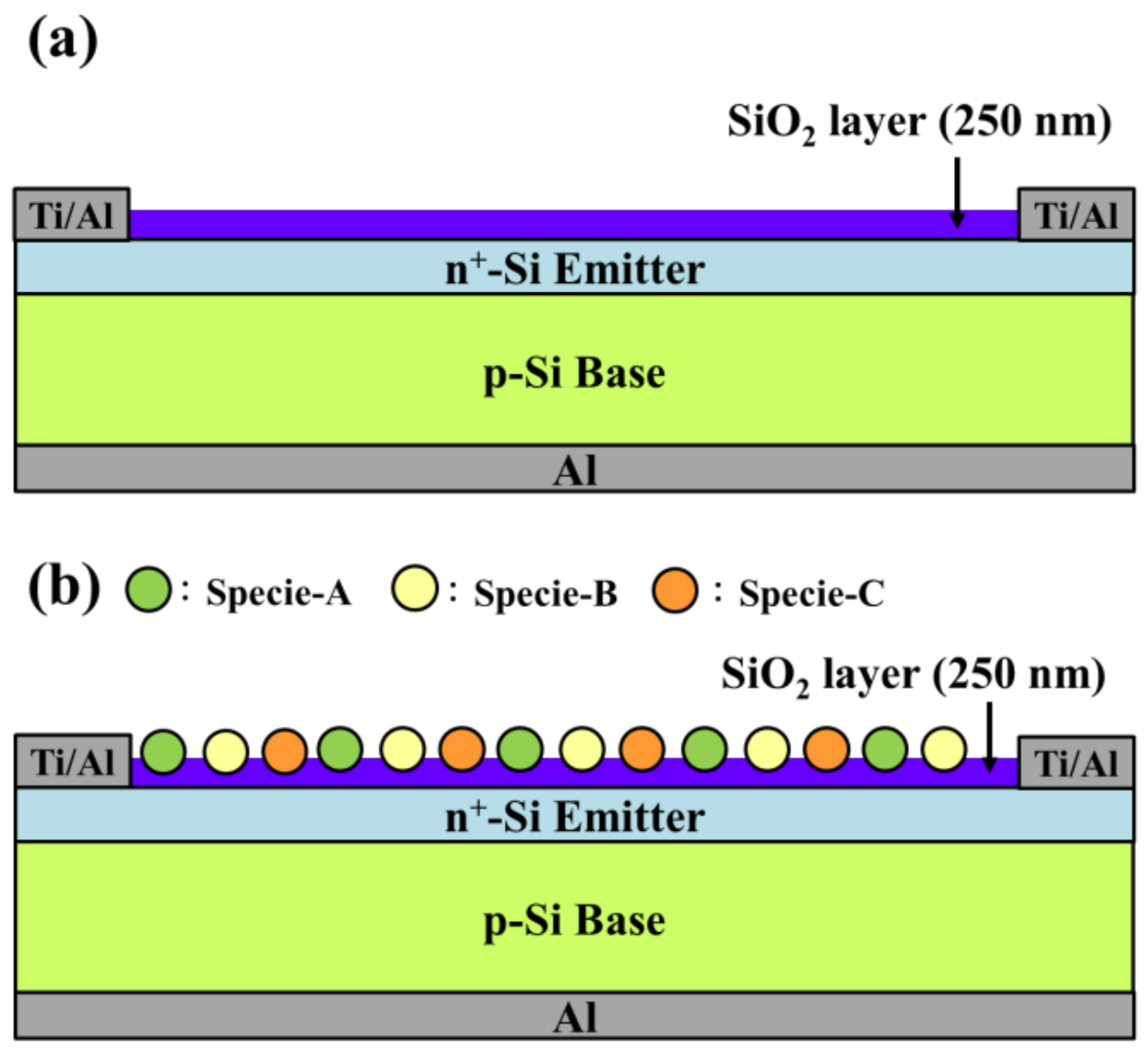
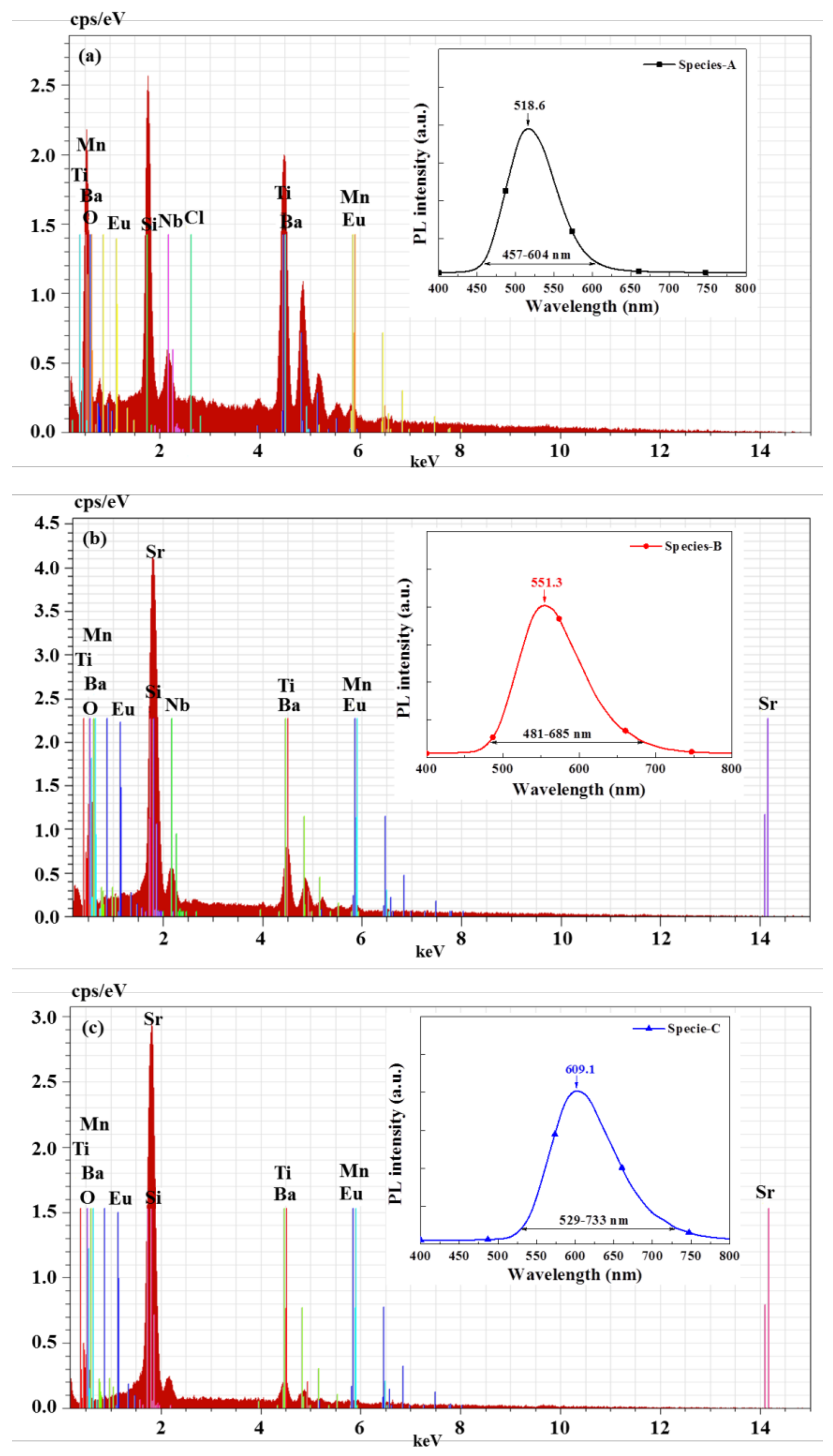
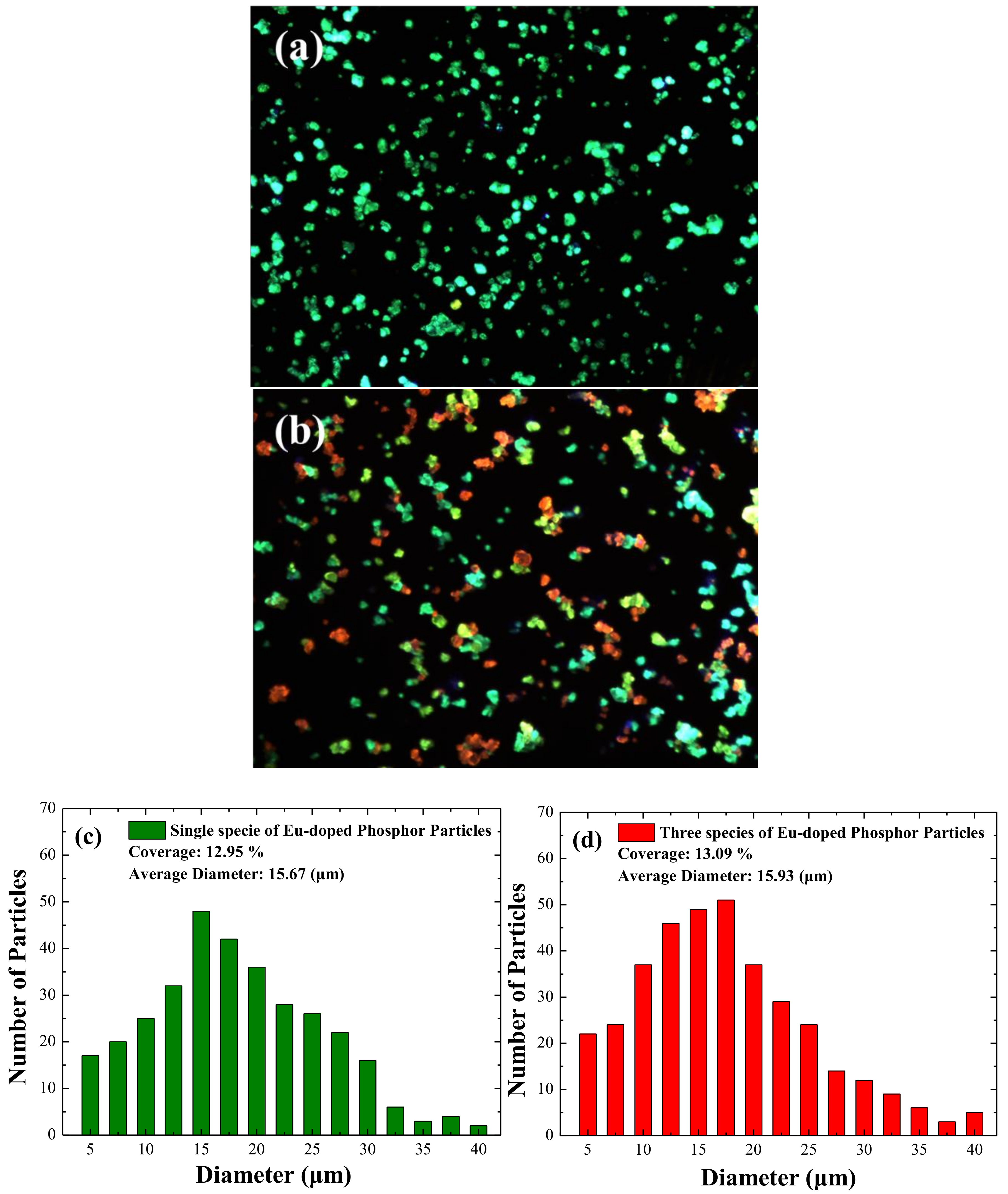
2.1. Deposition and Characterization of LDS Layer Comprising Three Species of Eu-Doped Silicate Phosphor
2.2. Fabrication and Characterization of Silicon Solar Cell Coated with LDS Layer Comprising Three Species of Eu-Doped Silicate Phosphor
3. Results and Discussion
4. Conclusions
Author Contributions
Funding
Acknowledgments
Conflicts of Interest
References
- Razykov, T.M.; Ferekides, C.S.; Morel, D.; Stefanakos, E.; Ullal, H.S.; Upadhyaya, H.M. Solar photovoltaic electricity: Current status and future prospects. Sol. Energy 2011, 85, 1580–1608. [Google Scholar] [CrossRef]
- Parida, B.; Iniyan, S.; Goic, R. A review of solar photovoltaic technologies. Renew. Sustain. Energy Rev. 2011, 15, 1625–1636. [Google Scholar] [CrossRef]
- Jäger-Waldau, A. PV Status Report 2017; JRC108105; Publications Office of the European Union: Luxembourg, 2017; Available online: https://www.researchgate.net/profile/Arnulf_Jaeger-Waldau/publication/321020820_PV_Status_Report_2017/links/5a08de1faca272ed279ff6c5/PV-Status-Report-2017.pdf (accessed on 27 April 2018).
- Green, M.A. Silicon solar cells: The ultimate photovoltaic solution? Prog. Photovolt. Res. Appl. 1994, 2, 87–94. [Google Scholar] [CrossRef]
- Couderc, R.; Amara, M.; Lemiti, M. In-depth analysis of heat generation in silicon solar cells. IEEE J. Photovolt. 2016, 6, 1123–1131. [Google Scholar] [CrossRef]
- Rajesh, C.; Pramod, M.R.; Patil, S.; Mahamuni, S.; More, S.; Dusane, R.O.; Ghaisas, S.V. Reduction in surface recombination through hydrogen and 1-heptene passivated silicon nanocrystals film on silicon solar cells. Sol. Energy 2012, 86, 489–495. [Google Scholar] [CrossRef]
- Belghachi, A. Detailed analysis of surface recombination in crystalline silicon solar cells. In Proceedings of the 2013 International Renewable and Sustainable Energy Conference (IRSEC), Ouarzazate, Morocco, 7–9 March 2013. [Google Scholar] [CrossRef]
- Alharbi, F.H.; Kais, S. Theoretical limits of photovoltaics efficiency and possible improvements by intuitive approaches learned from photosynthesis and quantum coherence. Renew. Sustain. Energy Rev. 2015, 43, 1073–1089. [Google Scholar] [CrossRef]
- Rühle, S. Tabulated values of the Shockley—Queisser limit for single junction solar cells. Sol. Energy 2016, 130, 139–147. [Google Scholar] [CrossRef]
- Queisser, H.J. Detailed balance limit for solar cell efficiency. Mater. Sci. Eng. B Solid State Mater. Adv. Technol. 2009, 159–160, 322–328. [Google Scholar] [CrossRef]
- Boriskina, S.V.; Chen, G. Exceeding the solar cell Shockley—Queisser limit via thermal up-conversion of low-energy photons. Opt. Commun. 2014, 314, 71–78. [Google Scholar] [CrossRef]
- Huang, X.Y.; Wang, J.X.; Yu, D.C.; Ye, S.; Zhang, Q.Y.; Sun, X.W. Spectral conversion for solar cell efficiency enhancement using YVO4:Bi3+,Ln3+ (Ln = Dy, Er, Ho, Eu, Sm, and Yb) phosphors. J. Appl. Phys. 2011, 109, 113526-1–113526-7. [Google Scholar] [CrossRef]
- Abrams, Z.R.; Niv, A.; Zhang, X. Solar energy enhancement using down-converting particles: A rigorous approach. J. Appl. Phys. 2011, 109, 114905-1–114905-9. [Google Scholar] [CrossRef]
- Solodovnyk, A.; Forberich, K.; Stern, E.; Krč, J.; Topič, M.; Batentschuk, M.; Lipovšek, B.; Brabec, C.J. Highly transmissive luminescent down-shifting layers filled with phosphor particles for photovoltaics. Opt. Mater. Express 2015, 5, 1296–1305. [Google Scholar] [CrossRef]
- Lipovšek, B.; Solodovnyk, A.; Forberich, K.; Stern, E; Krč, J.; Brabec, C.J.; Topič, M. Optical model for simulation and optimization of luminescent down-shifting layers filled with phosphor particles for photovoltaics. Opt. Express 2015, 23, A882–A895. [Google Scholar] [CrossRef]
- Gabr, A.M.; Walker, A.W.; Wilkins, M.M.; Kleiman, R.; Hinzer, K. Procedure to decouple reflectance and down-shifting effects in luminescent down-shifting enhanced photovoltaics. Opt. Express 2017, 25, A530–A538. [Google Scholar] [CrossRef] [PubMed]
- Yu, Y.; Lan, L.; Cai, H. Integrating down-shifting and down-conversion into metal−organic frameworks to enhance the spectral conversion for solar cells. J. Phys. Chem. C 2018, 122, 96–104. [Google Scholar] [CrossRef]
- Wang, C.Y.; Takeda, T.; Kate, O.M.; Xie, R.J.; Takahashi, K.; Hirosaki, N. Synthesis and photoluminescence properties of a phase pure green-emitting Eu doped JEM sialon (LaSi6−zAl1+zN10−zOz, z ~ 1) phosphor with a large red-shift of emission and unusual thermal quenching behavior. J. Mater. Chem. C 2016, 4, 10358–10366. [Google Scholar] [CrossRef]
- He, L.; Song, Z.; Jia, X.; Xia, Z.; Liu, Q. Control of luminescence in Eu2+-doped orthosilicate-orthophosphate phosphors by chainlike polyhedra and electronic structures. Inorg. Chem. 2018, 57, 609–616. [Google Scholar] [CrossRef] [PubMed]
- Hung, W.B.; Chen, J.Y.; Sung, K.W.; Chen, T.M. Enhanced conversion efficiency of crystalline Si solar cells via luminescent down-shifting using Ba2SiO4: Eu2+ phosphor. J. Ceram. Process. Res. 2014, 15, 157–161. [Google Scholar]
- Lima, S.M.; da Cunha Andrade, L.H.; Silva, J.R.; Bento, A.C.; Baesso, M.L.; Sampaio, J.A.; de Oliveira Nunes, L.A.; Guyot, Y.; Boulon, G. Broad combined orange-red emissions from Eu2+ and Eu3+-doped low-silica calcium aluminosilicate glass. Opt. Express 2012, 20, 12658–12665. [Google Scholar] [CrossRef] [PubMed]
- Chander, N.; Khan, A.F.; Chandrasekhar, P.S.; Thouti, E.; Swami, S.K.; Dutta, V.; Komarala, V.K. Reduced ultraviolet light induced degradation and enhanced light harvesting using YVO4:Eu3+ down-shifting nano-phosphor layer in organometal halide perovskite solar cells. Appl. Phys. Lett. 2014, 105, 033904-1–033904-5. [Google Scholar] [CrossRef]
- Shehata, N.; Clavel, M.; Meehan, K.; Samir, E.; Gaballah, S.; Salah, M. Enhanced erbium-doped ceria nanostructure coating to improve solar cell performance. Materials 2015, 8, 7663–7672. [Google Scholar] [CrossRef] [PubMed]
- Ho, W.J.; Yang, G.C.; Shen, Y.T.; Deng, Y.J. Improving efficiency of silicon solar cells using europium-doped silicate-phosphor layer by spin-on film coating. Appl. Surf. Sci. 2016, 365, 120–124. [Google Scholar] [CrossRef]
- Ho, W.J.; Shen, Y.T.; Deng, Y.J.; Yeh, C.W.; Sue, R.S. Performance enhancement of planar silicon solar cells through utilization of two luminescent down-shifting Eu-doped phosphor species. Thin Solid Films 2016, 618, 141–145. [Google Scholar] [CrossRef]
- Ho, W.J.; Shen, Y.T.; Liu, J.J.; You, B.J.; Ho, C.H. Enhancing photovoltaic performance using broadband luminescent down-shifting by combining multiple species of Eu-doped silicate phosphors. Nanomaterials 2017, 7, 340. [Google Scholar] [CrossRef] [PubMed]


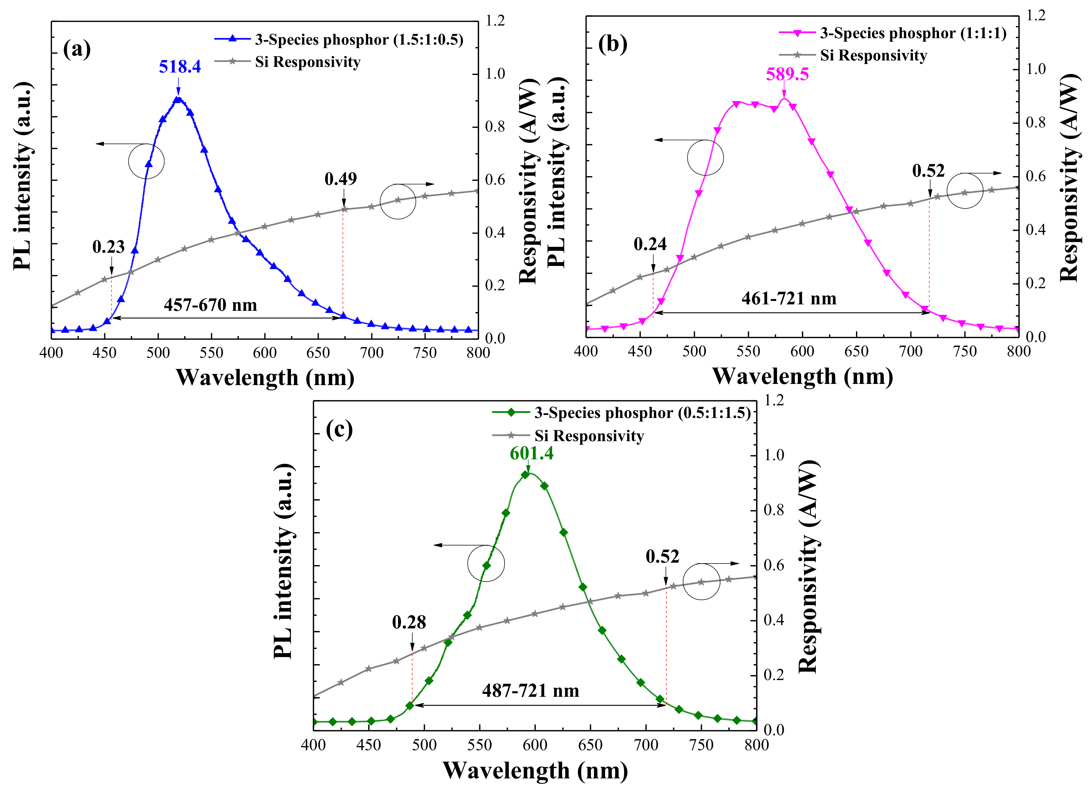
| Combination of Eu-Doped Phosphors | PL Emission Peak (nm) | PL Emission Wavelength Range (nm) @ 10% of Max. Intensity | Responsivity (A/W) Range @ 10% of Max. Intensity |
|---|---|---|---|
| Specie-A | 518.6 | 457–604 | 0.23–0.43 |
| Specie-B | 551.3 | 481–685 | 0.26–0.49 |
| Specie-C | 609.1 | 529–733 | 0.34–0.52 |
| 3-species phosphor (1.5:1:0.5) | 518.4 | 457–670 | 0.23–0.49 |
| 3-species phosphor (1:1:1) | 589.5 | 461–721 | 0.24–0.52 |
| 3-species phosphor (0.5:1:1.5) | 601.4 | 487–721 | 0.28–0.52 |
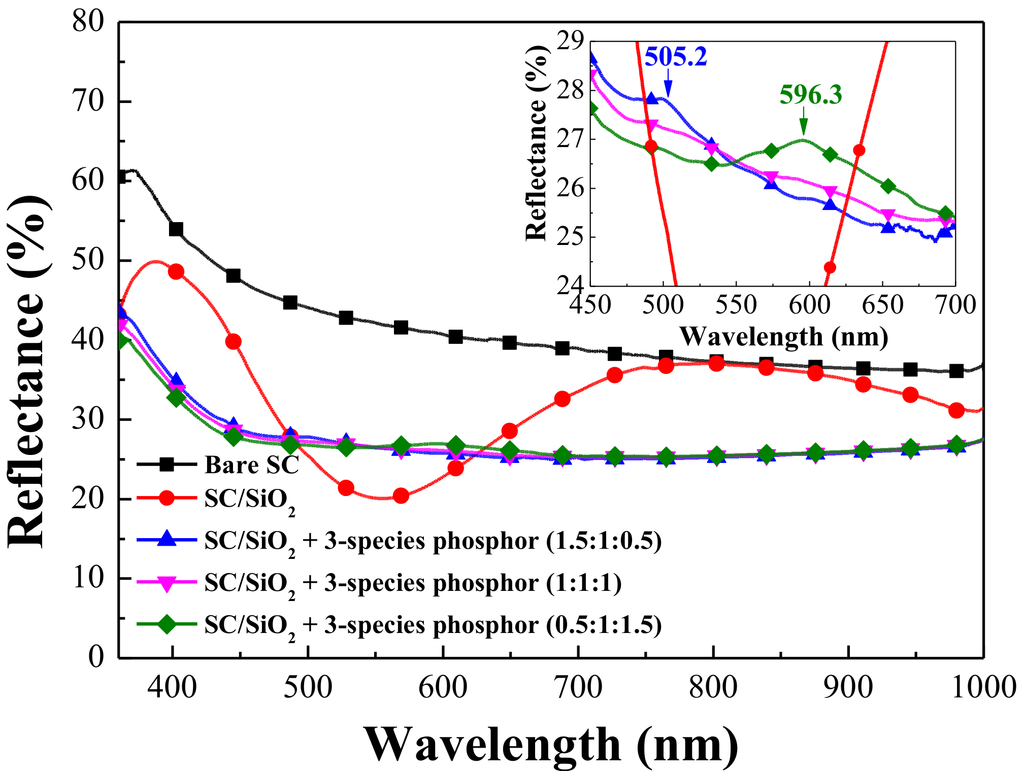
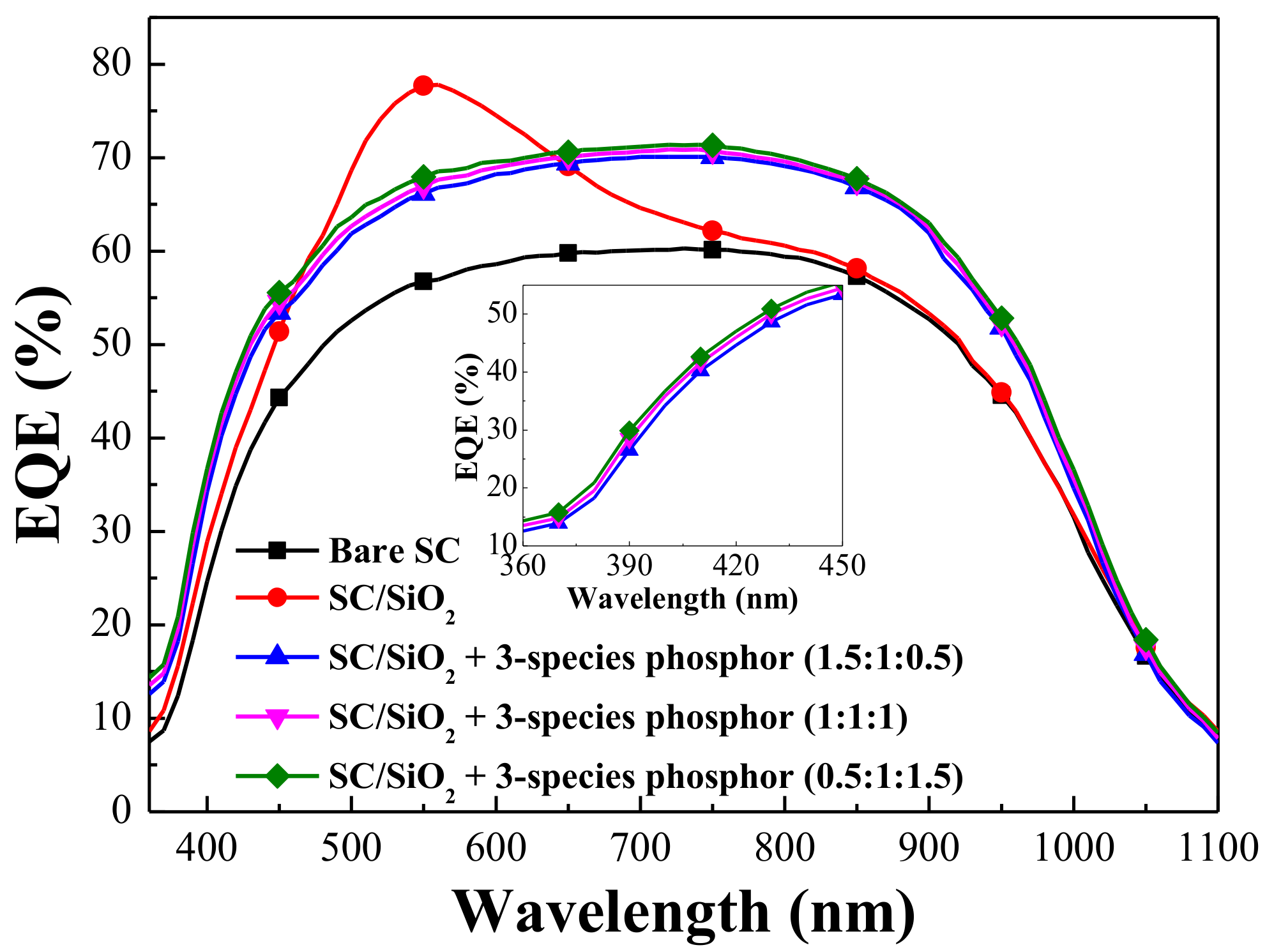
| Silicon Solar Cell | RW (%) @ 380–450 nm | RW (%) @ 380–1000 nm | EQEW (%) @ 380–450 nm | EQEW (%) @ 380–1000 nm |
|---|---|---|---|---|
| Bare Solar Cell (SC) | 51.69 | 41.23 | 32.77 | 50.51 |
| SC/SiO2 | 45.03 | 31.69 | 37.58 | 58.09 |
| SC/SiO2 + 3-species phosphor (1.5:1:0.5) | 32.26 | 27.03 | 42.03 | 59.76 |
| SC/SiO2 + 3-species phosphor (1:1:1) | 31.52 | 26.79 | 43.36 | 60.31 |
| SC/SiO2 + 3-species phosphor (0.5:1:1.5) | 30.72 | 26.63 | 44.44 | 60.99 |
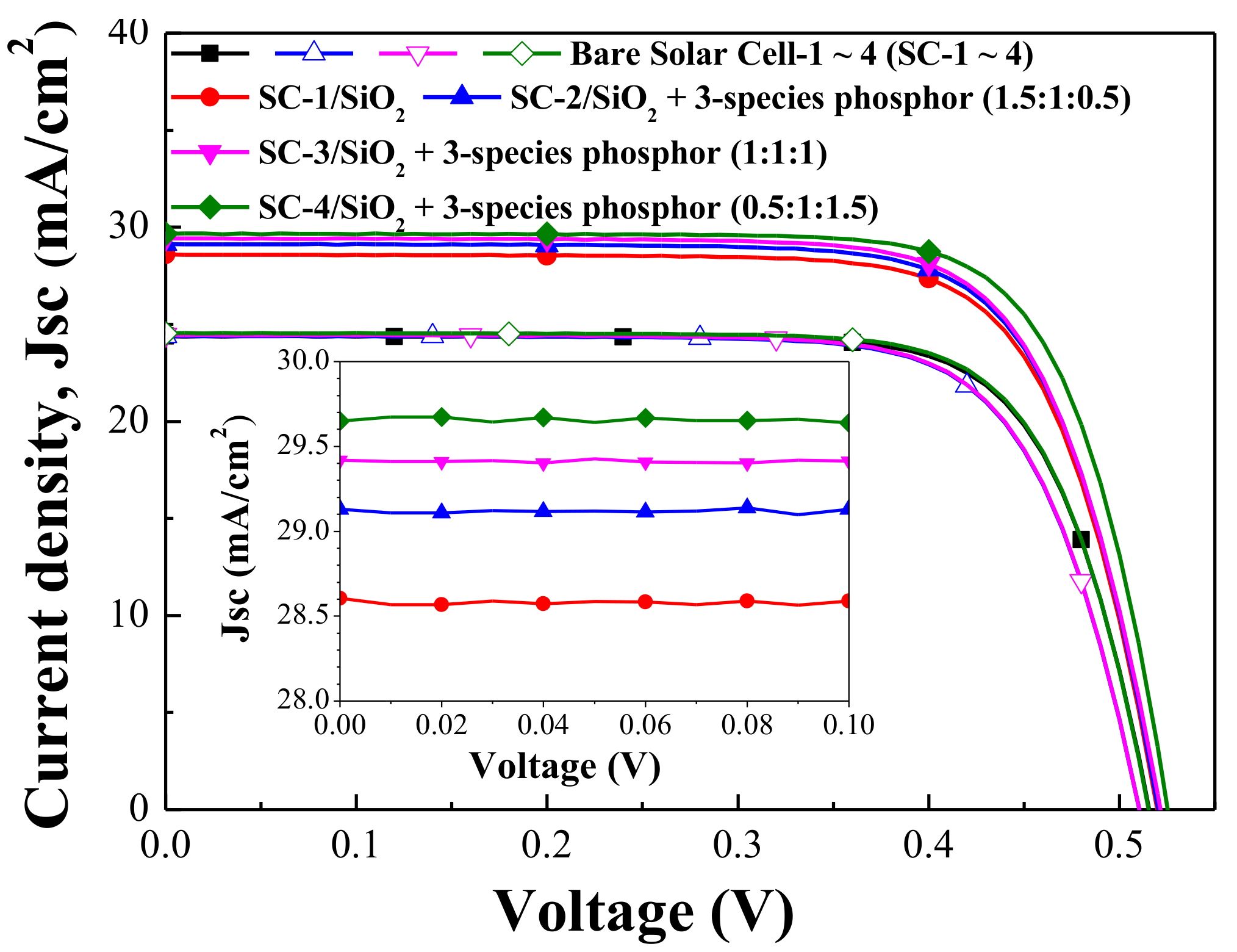
| Silicon Solar Cell | Voc (mV) | Jsc (mA/cm2) | Fill Factor (%) | η (%) | ΔJsc (%) | Δη (%) |
|---|---|---|---|---|---|---|
| Bare Solar Cell-1 (SC-1) | 518.4 | 24.56 | 73.45 | 9.35 | --- | --- |
| SC-1/ SiO2 | 522.2 | 27.71 | 73.54 | 10.64 | 12.83 | 13.80 |
| Bare Solar Cell-2 (SC-2) | 518.1 | 24.39 | 73.47 | 9.28 | --- | --- |
| SC-2/SiO2 + 3-species phosphor (1.5:1:0.5) | 522.9 | 28.36 | 73.12 | 10.84 | 16.27 | 16.81 |
| Bare Solar Cell-3 (SC-3) | 517.8 | 24.47 | 73.04 | 9.25 | --- | --- |
| SC-3/SiO2 + 3-species phosphor (1:1:1) | 524.8 | 28.80 | 73.24 | 11.07 | 17.70 | 19.67 |
| Bare Solar Cell-4 (SC-4) | 517.7 | 24.34 | 73.04 | 9.20 | --- | --- |
| SC-4/SiO2 + 3-species phosphor (0.5:1:1.5) | 524.7 | 28.92 | 73.05 | 11.08 | 18.81 | 20.43 |
© 2018 by the authors. Licensee MDPI, Basel, Switzerland. This article is an open access article distributed under the terms and conditions of the Creative Commons Attribution (CC BY) license (http://creativecommons.org/licenses/by/4.0/).
Share and Cite
Ho, W.-J.; You, B.-J.; Liu, J.-J.; Bai, W.-B.; Syu, H.-J.; Lin, C.-F. Photovoltaic Performance Enhancement of Silicon Solar Cells Based on Combined Ratios of Three Species of Europium-Doped Phosphors. Materials 2018, 11, 845. https://doi.org/10.3390/ma11050845
Ho W-J, You B-J, Liu J-J, Bai W-B, Syu H-J, Lin C-F. Photovoltaic Performance Enhancement of Silicon Solar Cells Based on Combined Ratios of Three Species of Europium-Doped Phosphors. Materials. 2018; 11(5):845. https://doi.org/10.3390/ma11050845
Chicago/Turabian StyleHo, Wen-Jeng, Bang-Jin You, Jheng-Jie Liu, Wen-Bin Bai, Hong-Jhang Syu, and Ching-Fuh Lin. 2018. "Photovoltaic Performance Enhancement of Silicon Solar Cells Based on Combined Ratios of Three Species of Europium-Doped Phosphors" Materials 11, no. 5: 845. https://doi.org/10.3390/ma11050845