Perovskites-Based Solar Cells: A Review of Recent Progress, Materials and Processing Methods

Abstract
:
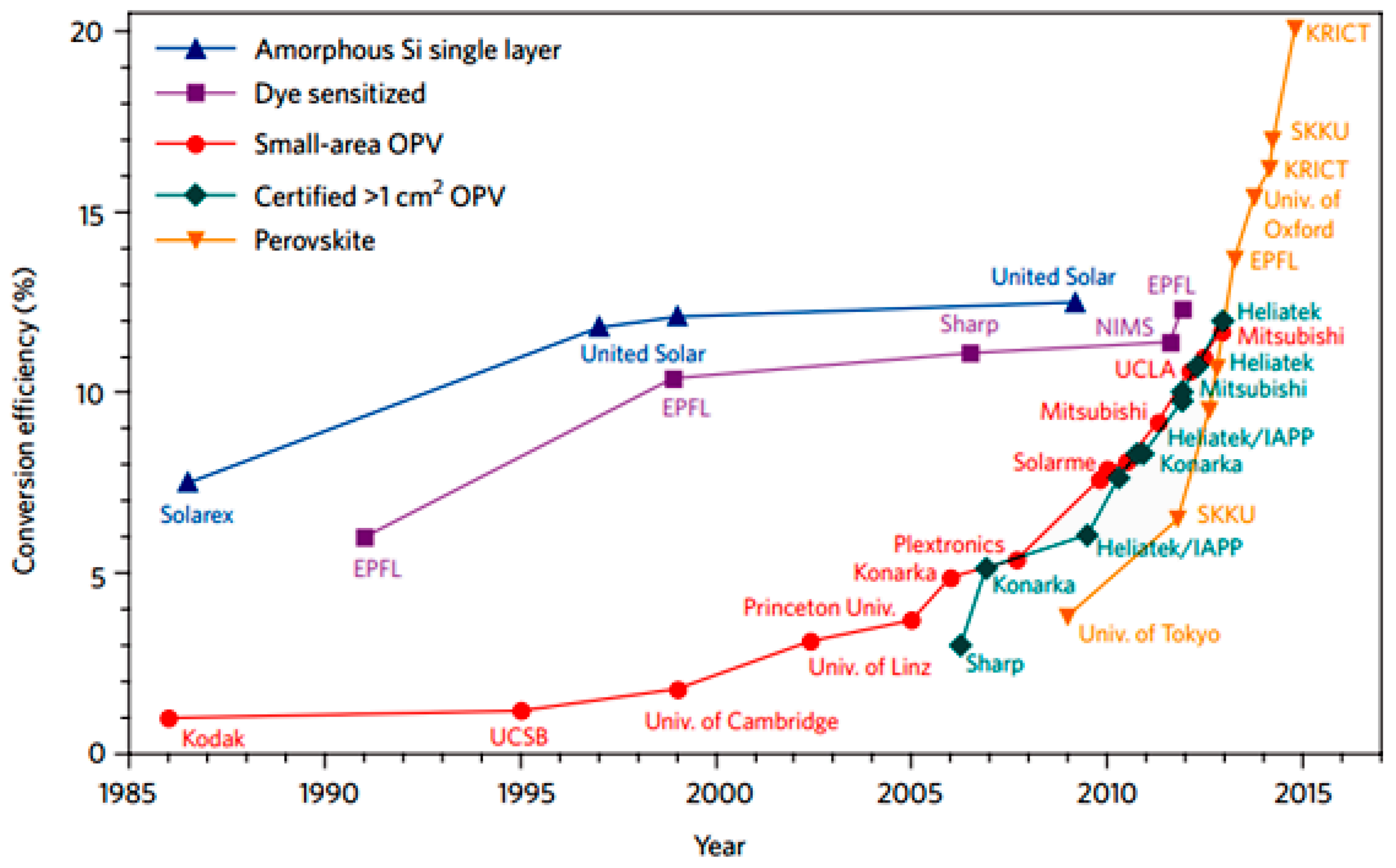
1. Introduction
2. Structures
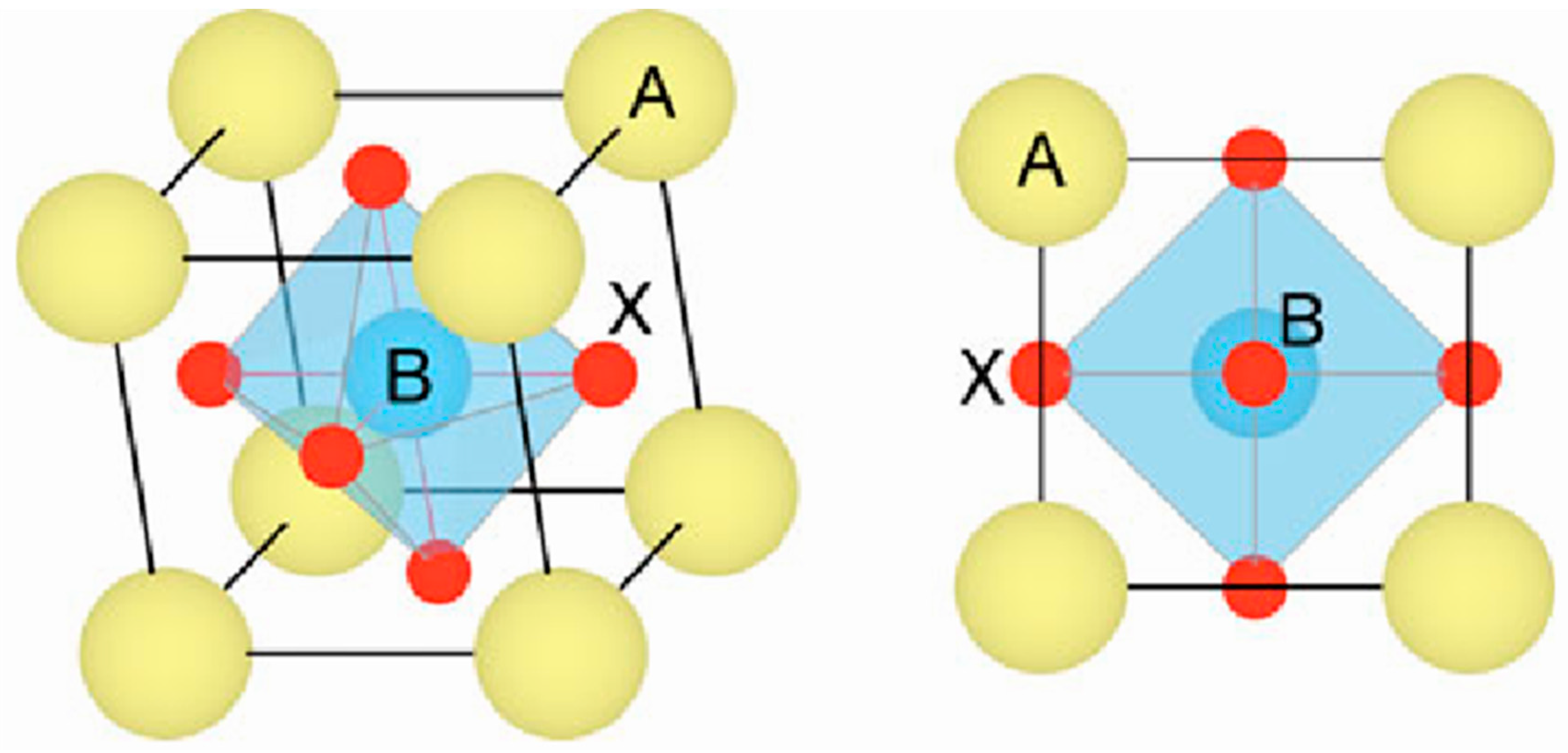
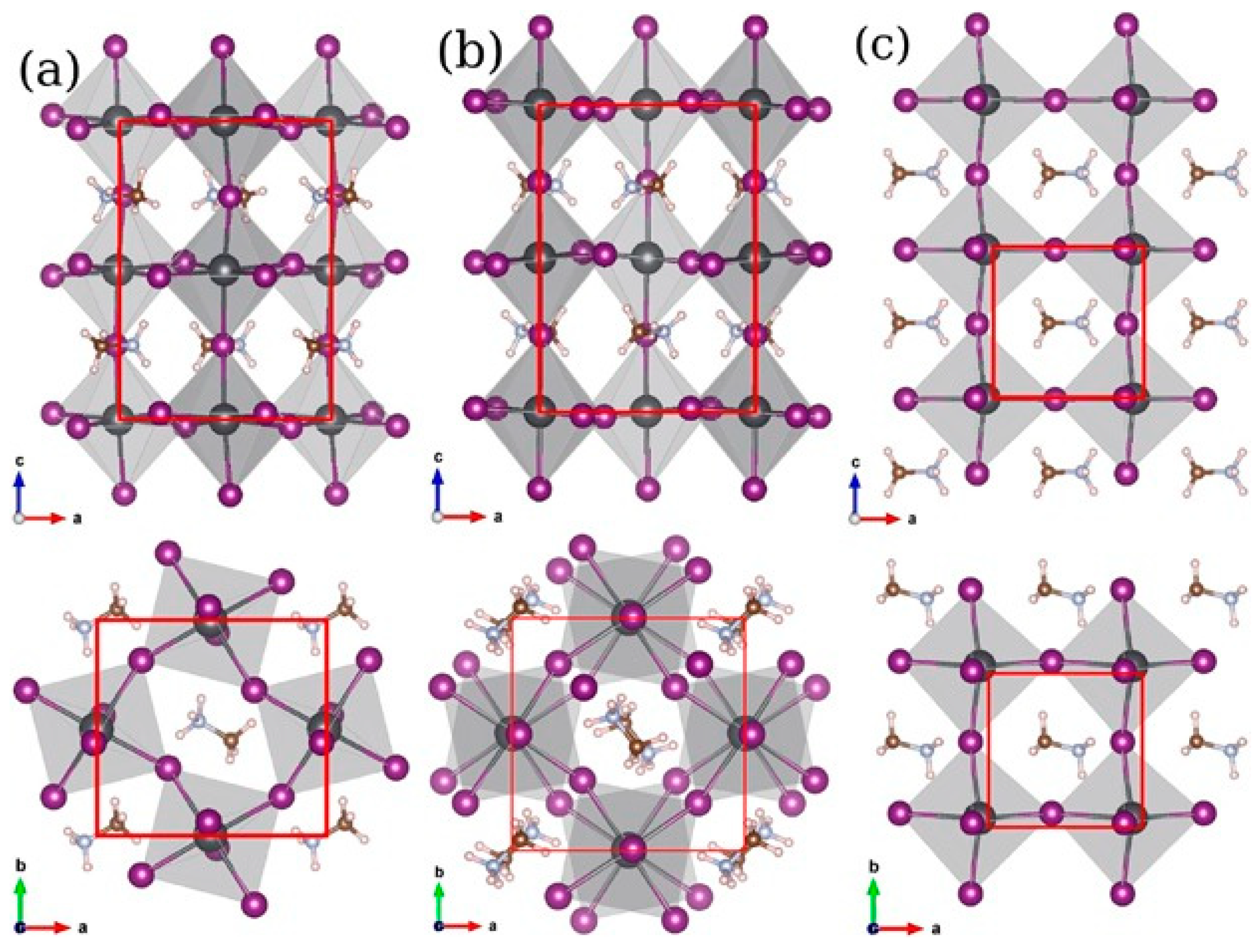
2.1. Crystal Structure
2.2. Electronic Structures
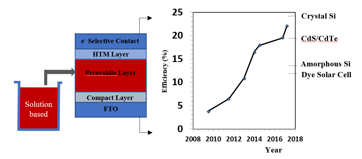
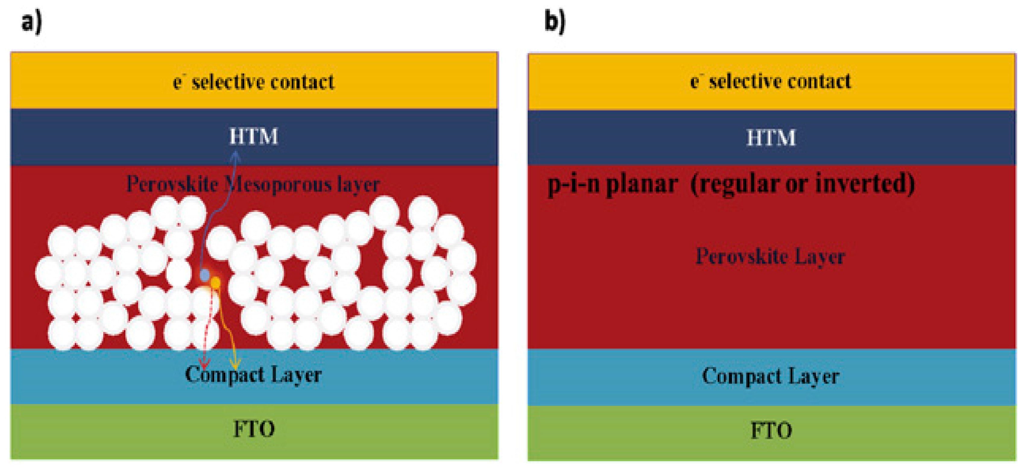
2.3. Device Structure
3. Fabrication Approaches
3.1. Perovskite Layer Fabrication
3.1.1. One-Step Method
3.1.2. Two-Step Method
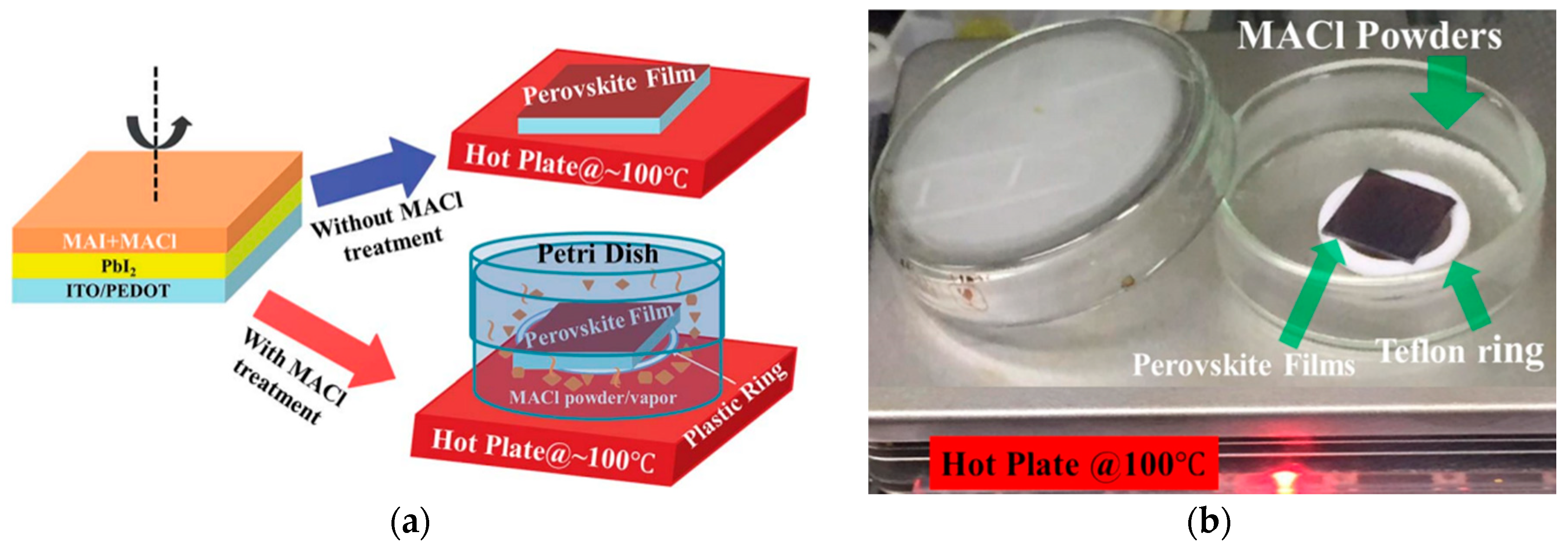
3.1.3. Vapor-Assisted Solution Method
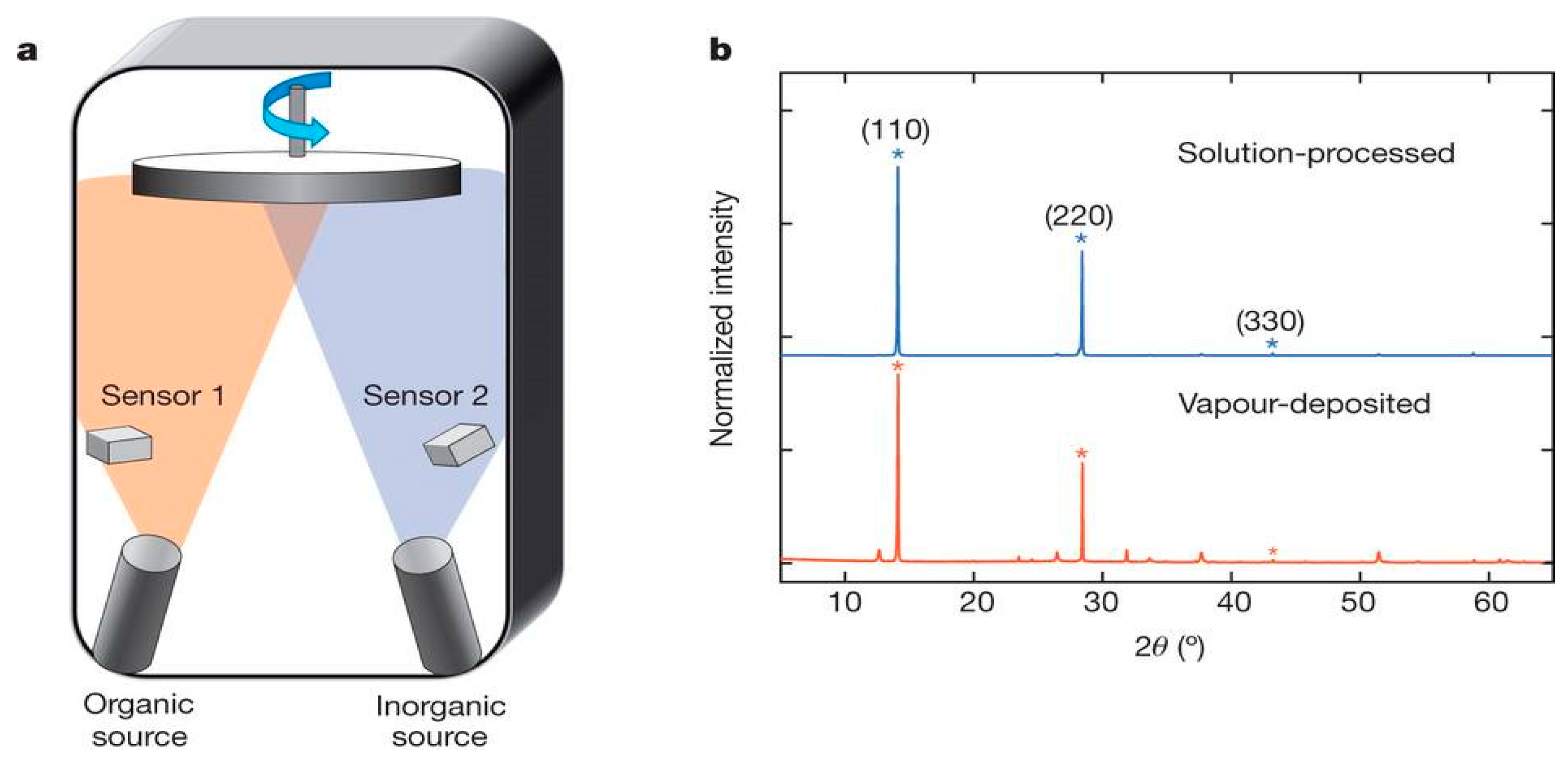
3.1.4. Thermal Vapor Deposition
3.2. Fabrication of Other Components in PSC
4. Challenges
4.1. Cell Stability
4.1.1. Stability of Perovskite Materials
Crystal Structure Stability
Environmental Stability
4.1.2. Stability of Other Components
4.2. J-V Hysteresis
5. Toxicity
6. Discussion and Future Research Efforts
7. Conclusions
Author Contributions
Acknowledgments
Conflicts of Interest
References
- Kojima, A.; Teshima, K.; Shirai, Y.; Miyasaka, T. Organometal halide perovskites as visible-light sensitizers for photovoltaic cells. J. Am. Chem. Soc. 2009, 131, 6050–6051. [Google Scholar] [CrossRef] [PubMed]
- Saliba, M.; Matsui, T.; Seo, J.Y.; Domanski, K.; Correa-Baena, J.P.; Nazeeruddin, M.K.; Zakeeruddin, S.M.; Tress, W.; Abate, A.; Hagfeldt, A.; et al. Cesium-containing triple cation PSCs: Improved stability, reproducibility and high efficiency. Energy Environ. Sci. 2016, 9, 1989–1997. [Google Scholar] [CrossRef] [PubMed]
- Yoshikawa, K.; Kawasaki, H.; Yoshida, W.; Irie, T.; Konishi, K.; Nakano, K.; Uto, T.; Adachi, D.; Kanematsu, M.; Uzu, H.; et al. Silicon heterojunction solar cell with interdigitated back contacts for a photoconversion efficiency over 26%. Nat. Energy 2017, 2, 17032. [Google Scholar] [CrossRef]
- Jeon, N.J.; Noh, J.H.; Yang, W.S.; Kim, Y.C.; Ryu, S.; Seo, J.; Seok, S.I. Compositional engineering of perovskite materials for high-performance solar cells. Nature 2015, 517, 476–480. [Google Scholar] [CrossRef] [PubMed]
- Park, N.G. PSCs: An emerging photovoltaic technology. Mater. Today 2015, 18, 65–72. [Google Scholar] [CrossRef]
- Green, M.A.; Baillie, A.H.; Snaith, H.J. The emergence of PSCs. Nat. Photonics 2014, 8, 506–514. [Google Scholar] [CrossRef]
- Rangel-Cárdenas, J.; Sobral, H. Optical absorption enhancement in CdTe thin films by microstructuration of the silicon substrate. Materials 2017, 10, 607. [Google Scholar] [CrossRef] [PubMed]
- Shi, Z.; Jayatissa, A.H. One-pot hydrothermal synthesis and fabrication of kesterite Cu2ZnSn(S,Se)4 thin films. Prog. Nat. Sci. Mater. Int. 2017, 27, 550–555. [Google Scholar] [CrossRef]
- Kumar, M.H.; Yantara, N.; Dharani, S.; Graetzel, M.; Mhaisalkar, S.; Boix, P.P.; Mathews, N. Flexible, low-temperature, solution processed ZnO-based perovskite solid state solar cells. Chem. Commun. 2013, 49, 11089–11091. [Google Scholar] [CrossRef] [PubMed]
- Shin, S.S.; Yang, W.S.; Noh, J.H.; Suk, J.H.; Jeon, N.J.; Park, J.H.; Kim, J.S.; Seong, W.M.; Seok, S.I. High-performance flexible PSCs exploiting Zn2SnO4 prepared in solution below 100 °C. Nat. Commun. 2015, 6, 7410. [Google Scholar] [CrossRef] [PubMed]
- Liu, D.; Kelly, T.L. PSCs with a planar heterojunction structure prepared using room-temperature solution processing techniques. Nat. Photonics 2014, 8, 133–138. [Google Scholar] [CrossRef]
- Im, J.H.; Lee, C.R.; Lee, J.W.; Park, S.W.; Park, N.G. 6.5% efficient perovskite quantum-dot-sensitized solar cell. Nanoscale 2011, 3, 4088–4093. [Google Scholar] [CrossRef] [PubMed]
- Lee, M.M.; Teuscher, J.; Miyasaka, T.; Murakami, T.N.; Snaith, H.J. Efficient hybrid solar cells based on meso-superstructured organometal halide perovskites. Science 2012, 338, 643–647. [Google Scholar] [CrossRef] [PubMed]
- Wang, J.T.W.; Ball, J.M.; Barea, E.M.; Abate, A.; Alexander-Webber, J.A.; Huang, J.; Saliba, M.; Mora-Sero, I.; Bisquert, J.; Snaith, H.J. Low-temperature processed electron collection layers of graphene/TiO2 nanocomposites in t hin film PSCs. Nano Lett. 2014, 14, 724–730. [Google Scholar] [CrossRef] [PubMed]
- Yang, W.S.; Noh, J.H.; Jeon, N.J.; Kim, Y.C.; Ryu, S.; Seo, J.; Seok, S.I. High-performance photovoltaic perovskite layers fabricated through intramolecular exchange. Science 2015, 348, 1234–1237. [Google Scholar] [CrossRef] [PubMed]
- Cao, J.; Wu, B.; Chen, R.; Wu, Y.; Hui, Y.; Mao, B.W.; Zheng, N. Efficient, hysteresis-free and stable perovskite solar cells with ZnO as electron-transport layer: effect of surface passivation. Adv. Mater. 2018, 30, 1705596. [Google Scholar] [CrossRef] [PubMed]
- Shin, S.S.; Yeom, E.J.; Yang, W.S.; Hur, S.; Kim, M.G.; Im, J.; Seo, J.; Noh, J.H.; Seok, S.I. Colloidally prepared La-doped BaSnO3 electrodes for efficient, photostable PSCs. Science 2017, 356, 167–171. [Google Scholar] [CrossRef] [PubMed]
- Ramírez Quiroz, C.O.; Shen, Y.; Salvador, M.; Forberich, K.; Schrenker, N.; Spyropoulos, G.D.; Heumüller, T.; Wilkinson, B.; Kirchartz, T.; Spiecker, E.; et al. Balancing electrical and optical losses for efficient 4-terminal Si–PSCs with solution processed percolation electrodes. J. Mater. Chem. A 2018, 6, 3583. [Google Scholar] [CrossRef]
- Leo, K. Perovskite photovoltaics: signs of stability. Nat. Nanotechnol. 2015, 10, 574–575. [Google Scholar] [CrossRef] [PubMed]
- Grånäs, O.; Vinichenko, D.; Kaxiras, E. Establishing the limits of efficiency of PSCs from first principles modeling. Sci. Rep. 2016, 6, 36108. [Google Scholar] [CrossRef] [PubMed]
- Berhe, T.A.; Su, W.N.; Chen, C.H.; Pan, C.J.; Cheng, J.H.; Chen, H.M.; Tsai, M.C.; Chen, L.Y.; Dubale, A.A.; Hwang, B.J. Organometal halide PSCs: Degradation and stability. Energy Environ. Sci. 2016, 9, 323–356. [Google Scholar] [CrossRef]
- Chen, W.; Wu, Y.; Yue, Y.; Liu, J.; Zhang, W.; Yang, X.; Chen, H.; Bi, E.; Ashraful, I.; Grätzel, M.; Han, L. Efficient and stable large-area PSCs with inorganic charge extraction layers. Science 2015, 350, 944–948. [Google Scholar] [CrossRef] [PubMed]
- Unger, E.L.; Hoke, E.T.; Bailie, C.D.; Nguyen, W.H.; Bowring, A.R.; Heumüller, T.; Christoforo, M.G.; McGehee, M.D. Hysteresis and transient behavior in current–voltage measurements of hybrid-perovskite absorber solar cells. Energy Environ. Sci. 2014, 7, 3690–3698. [Google Scholar] [CrossRef]
- Osterwald, C.R.; McMahon, T.J. History of accelerated and qualification testing of terrestrial photovoltaic modules: A literature review. Prog. Photovolt Res. Appl. 2009, 17, 11–33. [Google Scholar] [CrossRef]
- Zhou, D.; Zhou, T.; Tian, Y.; Zhu, X.; Tu, Y. Perovskite-based solar cells: Materials, methods and future perspectives. J. Nanomater. 2018, 2018, 8148072. [Google Scholar] [CrossRef]
- Zuo, C.; Ding, L. Lead-free perovskite materials (NH4)3Sb2IxBr9−x. Angew. Chem. Int. Ed. 2017, 56, 6528–6532. [Google Scholar] [CrossRef] [PubMed]
- Hao, F.; Stoumpos, C.C.; Cao, D.H.; Chang, R.P.H.; Kanatzidis, M.G. Lead-free solid-state organic–inorganic halide PSCs. Nat. Photonics 2014, 8, 489–494. [Google Scholar] [CrossRef]
- Sun, Y.Y.; Shi, J.; Lian, J.; Gao, W.; Agiorgousis, M.L.; Zhang, P.; Zhang, S. Discovering lead-free perovskite solar materials with a split-anion approach. Nanoscale 2016, 8, 6284–6289. [Google Scholar] [CrossRef] [PubMed]
- Conings, B.; Baeten, L.; De Dobbelaere, C.; D’Haen, J.; Manca, J.; Boyen, H. Perovskite-based hybrid solar cells exceeding 10% efficiency with high reproducibility using a thin film sandwich approach. Adv. Mater. 2014, 26, 2041–2046. [Google Scholar] [CrossRef] [PubMed]
- Tan, K.W.; Moore, D.T.; Saliba, M.; Sai, H.; Estroff, L.A.; Hanrath, T.; Snaith, H.J.; Wiesner, U. Thermally induced structural evolution and performance of mesoporous block copolymer-directed alumina PSCs. ACS Nano 2014, 8, 4730–4739. [Google Scholar] [CrossRef] [PubMed]
- Jain, A.; Castelli, I.E.; Hautier, G.; Bailey, D.H.; Jacobson, K.W. Performance of genetic algorithms in search for water splitting perovskites. J. Mater. Sci. 2013, 48, 6519–6534. [Google Scholar] [CrossRef]
- Kawamura, Y.; Mashiyama, H.; Hasebe, K. Structural study on cubic–tetragonal transition of CH3NH3PbI3. J. Phys. Soc. Jpn. 2002, 71, 1694–1697. [Google Scholar] [CrossRef]
- Whitfield, P.S.; Herron, N.; Guise, W.E.; Page, K.; Cheng, Y.Q.; Milas, I.; Crawford, M.K. Structures, Phase transitions and tricritical behavior of the hybrid perovskite methyl ammonium lead iodide. Sci. Rep. 2016, 6, 35685. [Google Scholar] [CrossRef] [PubMed]
- Bischak, C.G.; Hetherington, C.L.; Wu, H.; Aloni, S.; Ogletree, D.F.; Limmer, D.T.; Ginsberg, N.S. Origin of reversible photoinduced phase separation in hybrid perovskites. Nano Lett. 2017, 17, 1028–1033. [Google Scholar] [CrossRef] [PubMed]
- Korshunova, K.; Winterfeld, L.; Beenken, W.J.D.; Runge, E. Thermodynamic stability of mixed Pb:Sn methyl-ammonium halide perovskites. Phys. Status Solidi 2016, 253, 1907–1915. [Google Scholar] [CrossRef]
- Zhou, Y.; Huang, F.; Cheng, Y.; Weale, A.G. Photovoltaic performance and the energy landscape of CH3NH3PbI3. Phys. Chem. Chem. Phys. 2015, 17, 22604–22615. [Google Scholar] [CrossRef] [PubMed]
- Brenner, T.M.; Egger, D.A.; Kronik, L.; Hodes, G.; Cahen, D. Hybrid organic—Inorganic perovskites: Low-cost semiconductors with intriguing charge-transport properties. Nat. Rev. Mater. 2016, 1, 1–16. [Google Scholar] [CrossRef]
- Tanaka, K.; Takahashi, T.; Ban, T.; Kondo, T.; Uchida, K.; Miura, N. Comparative study on the excitons in lead-halide-based perovskite-type crystals CH3NH3PbBr3 CH3NH3PbI3. Solid State Commun. 2003, 127, 619–623. [Google Scholar] [CrossRef]
- Wehrenfennig, C.; Eperon, G.E.; Johnston, M.B.; Snaith, H.J.; Herz, L.M. High charge carrier mobilities and lifetimes in organolead trihalide perovskites. Adv. Mater. 2014, 26, 1584–1589. [Google Scholar] [CrossRef] [PubMed]
- Brandt, R.; Stevanović, V.; Ginley, D.; Buonassisi, T. Identifying defect-tolerant semiconductors with high minority-carrier lifetimes: Beyond hybrid lead halide perovskites. MRS Commun. 2015, 5, 265–275. [Google Scholar] [CrossRef]
- Oga, H.; Saeki, A.; Ogomi, Y.; Hayase, S.; Seki, S. Improved understanding of the electronic and energetic landscapes of PSCs: High local charge carrier mobility, reduced recombination and extremely shallow traps. J. Am. Chem. Soc. 2014, 136, 13818–13825. [Google Scholar] [CrossRef] [PubMed]
- Savenije, T.J.; Ponseca, C.S., Jr.; Kunneman, L.; Abdellah, M.; Zheng, K.; Tian, Y.; Zhu, Q.; Canton, S.E.; Scheblykin, I.G.; Pullerits, T.; et al. Thermally activated exciton dissociation and recombination control the carrier dynamics in organometal halide perovskite. J. Phys. Chem. Lett. 2014, 5, 2189–2194. [Google Scholar] [CrossRef] [PubMed]
- Dong, Q.; Fang, Y.; Shao, Y.; Mulligan, P.; Qiu, J.; Cao, L.; Huang, J. Solar cells. Electron-hole diffusion lengths>175 μm in solution-grown CH3NH3PbI3 single crystals. Science 2015, 347, 967–970. [Google Scholar] [CrossRef] [PubMed]
- Diffusion Length-PV Education. Org. Available online: http://www.pveducation.org/pvcdrom/diffusion-length (accessed on 2 May 2018).
- GaAs-Gallium Arsenide Electrical properties. Available online: http://www.ioffe.ru/SVA/NSM/Semicond/GaAs/electric.html (accessed on 2 May 2018).
- Handloser, K.; Giesbrecht, N.; Bein, T.; Docampo, P.; Handloser, M.; Hartschuh, A. Contactless visualization of fast charge carrier diffusion in hybrid halide perovskite thin films. ACS Photonics 2016, 3, 255–261. [Google Scholar] [CrossRef]
- Ciesielski, R.; Schäfer, F.; Hartmann, N.F.; Giesbrecht, N.; Bein, T.; Docampo, P.; Hartschuh, A. Grain boundaries act as solid walls for charge carrier diffusion in large crystal MAPI thin films. ACS Appl. Mater. Interfaces 2018, 10, 7974–7981. [Google Scholar] [CrossRef] [PubMed]
- Liu, X.; Zhao, W.; Cui, H.; Xie, Y.; Wang, Y.; Xu, T.; Huang, F. Organic–inorganic halide perovskite based solar cells-revolutionary progress in photovoltaics. Inorg. Chem. Front. 2015, 2, 315. [Google Scholar] [CrossRef]
- Eperon, G.E.; Burlakov, V.M.; Docampo, P.; Goriely, A.; Snaith, H.J. Morphological control for high performance, solution-processed planar heterojunction PSCs. Adv. Funct. Mater. 2014, 24, 151–157. [Google Scholar] [CrossRef]
- Anaraki, E.H.; Kermanpur, A.; Steier, L.; Domanski, K.; Matsui, T.; Tress, W.; Saliba, M.; Abate, A.; Gratzel, M.; Hagfeldt, A.; et al. Highly efficient and stable planar PSCs by solution-processed tin oxide. Energy Environ. Sci. 2016, 9, 3128–3134. [Google Scholar] [CrossRef]
- Correa-Baena, J.-P.; Saliba, M.; Buonassisi, T.; Grätzel, M.; Abate, A.; Tress, W.; Hagfeldt, A. Promises and challenges of perovskite solar cells. Science 2017, 358, 739–744. [Google Scholar] [CrossRef] [PubMed]
- Cui, J.; Yuan, H.; Li, J.; Xu, X.; Shen, Y.; Lin, H.; Wang, M. Recent progress in efficient hybrid lead halide PSCs. Sci. Technol. Adv. Mater. 2015, 16, 036004. [Google Scholar] [CrossRef] [PubMed]
- Saliba, M.; Matsui, T.; Domanski, K.; Seo, J.-Y.; Ummadisingu, A.; Zakeeruddin, S.M.; Correa-Baena, J.P.; Tress, W.R.; Abate, A.; Hagfeldt, A.; et al. Incorporation of rubidium cations into PSCs improves photovoltaic performance. Science 2016, 354, 206–209. [Google Scholar] [CrossRef] [PubMed]
- Saliba, M.; Correa-Baena, J.-P.; Grätzel, M.; Hagfeldt, A.; Abate, A. Perovskite solar cells: From the atomic level to film quality and device performance. Angew. Chem. Int. Ed. 2018, 57, 2554–2569. [Google Scholar] [CrossRef] [PubMed]
- Jeon, N.J.; Noh, J.H.; Kim, Y.C.; Yang, W.S.; Ryu, S.; Seok, S.I. Solvent engineering for high-performance inorganic-organic hybrid PSCs. Nat. Mater. 2014, 13, 897–903. [Google Scholar] [CrossRef] [PubMed]
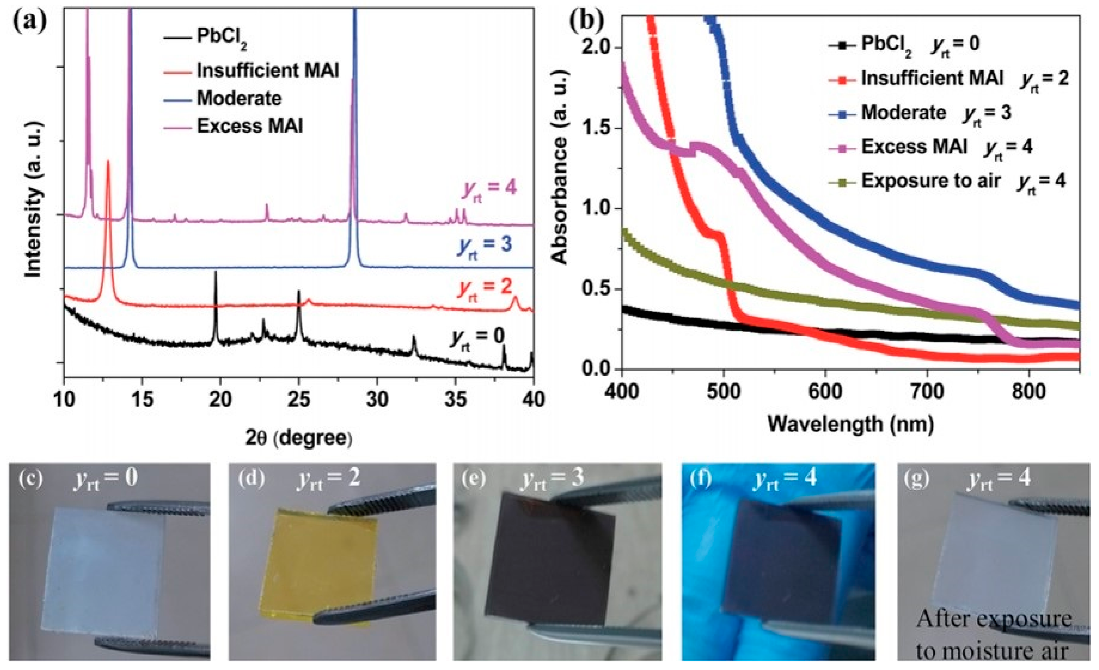
- Rong, Y.; Venkatesan, S.; Guo, R.; Wang, Y.; Bao, J.; Li, W.; Fan, Z.; Yao, Y. Critical kinetic control of non-stoichiometric intermediate phase transformation for efficient PSCs. Nanoscale 2016, 8, 12892. [Google Scholar] [CrossRef] [PubMed]
- Guo, X.; McCleese, C.; Kolodziej, C.; Samia, A.C.S.; Zhao, Y.; Burda, C. Identification and characterization of the intermediate phase in hybrid organic–inorganic MAPbI3 perovskite. Dalton Trans. 2016, 45, 3806. [Google Scholar] [CrossRef] [PubMed]
- Guo, Y.; Shoyama, K.; Sato, W.; Matsuo, Y.; Inoue, K.; Harano, K.; Liu, C.; Tanaka, H.; Nakamura, E. Chemical pathways connecting lead(II) iodide and perovskite via polymeric plumbate(II) fiber. J. Am. Chem. Soc. 2015, 137, 15907–15914. [Google Scholar] [CrossRef] [PubMed]
- Ren, Y.; Liu, S.; Duan, B.; Xu, Y.F.; Li, Z.Q.; Huang, Y.; Hu, L.H.; Zhu, J.; Dai, S.Y. Controllable intermediates by molecular self-assembly for optimizing the fabrication of large-grain perovskite films via one-step spin-coating. J. Alloys Compd. 2017, 705, 205–210. [Google Scholar] [CrossRef]
- Liang, P.W.; Liao, C.Y.; Chueh, C.C.; Zuo, F.; Williams, S.T.; Xin, X.K.; Lin, J.; Jen, A.K.Y. Additive enhanced crystallization of solution-processed perovskite for highly efficient planar-heterojunction solar cells. Adv. Mater. 2014, 26, 3748–3754. [Google Scholar] [CrossRef] [PubMed]
- Chen, Y.; Zhao, Y.; Liang, Z. Non-thermal annealing fabrication of efficient planar PSCs with inclusion of NH4Cl. Chem. Mater. 2015, 27, 1448–1451. [Google Scholar] [CrossRef]
- Heo, J.H.; Song, D.H.; Han, H.J.; Kim, S.Y.; Kim, J.H.; Kim, D.; Shin, H.W.; Ahn, T.K.; Wolf, C.; Lee, T.W.; et al. Planar CH3NH3PbI3 PSCs with constant 17.2% average power conversion efficiency irrespective of the scan rate. Adv. Mater. 2015, 27, 3424–3430. [Google Scholar] [CrossRef] [PubMed]
- Zhao, Y.; Zhu, K. Efficient planar PSCs based on 1.8 eV band gap CH3NH3PbI2Br nanosheets via thermal decomposition. J. Am. Chem. Soc. 2014, 136, 12241–12244. [Google Scholar] [CrossRef] [PubMed]
- Zhang, Y.; Grancini, G.; Feng, Y.; Asiri, A.M.; Nazeeruddin, M.K. Optimization of stable quasi-cubic FAxMA1−xPbI3 perovskite structure for solar cells with efficiency beyond 20%. ACS Energy Lett. 2017, 2, 802–806. [Google Scholar] [CrossRef]
- Ansari, M.I.H.; Qurashi, A.; Nazeeruddin, M.K. Frontiers, opportunities and challenges in perovskite solar cells: A critical review. J Photochem. Photobiol. C 2018, 35, 1–24. [Google Scholar] [CrossRef]
- Eperon, G.E.; Stranks, S.D.; Menelaou, C.; Johnston, M.B.; Herz, L.M.; Snaith, H.J. Formamidinium lead trihalide: a broadly tunable perovskite for efficient planar heterojunction solar cells. Energy Environ. Sci. 2014, 7, 982–988. [Google Scholar] [CrossRef]
- Pellet, N.; Gao, P.; Gregori, G.; Yang, T.Y.; Nazeeruddin, M.K.; Maier, J.; Grätzel, M. Mixed-organic-cation perovskite photovoltaics for enhanced solar-light harvesting. Angew. Chem. Int. Ed. 2014, 53, 3151–3157. [Google Scholar] [CrossRef] [PubMed]
- Back, H.; Kim, J.; Kim, G.; Kim, T.K.; Kang, H.; Kong, J.; Lee, S.H.; Lee, K. Interfacial modification of hole transport layers for efficient large-area PSCs achieved via blade-coating. Sol. Energy Mater. Sol. Cells 2016, 144, 309–315. [Google Scholar] [CrossRef]
- Chen, H.; Wei, Z.; Zheng, X.; Yang, S. A scalable electrodeposition route to the low-cost, versatile and controllable fabrication of PSCs. Nano Energy 2015, 15, 216–226. [Google Scholar] [CrossRef]
- Li, S.G.; Jiang, K.J.; Su, M.J.; Cui, X.P.; Huang, J.H.; Zhang, Q.Q.; Zhou, X.Q.; Yang, L.M.; Song, Y.L. Inkjet printing of CH3NH3PbI3 on a mesoscopic TiO2 film for highly efficient PSCs. J. Mater. Chem. A 2015, 3, 9092–9097. [Google Scholar] [CrossRef]
- Hwang, K.; Jung, Y.; Heo, Y.; Scholes, F.H.; Watkins, S.E.; Subbiah, J.; Jones, D.J.; Kim, D.Y.; Vak, D. Toward large scale roll-to-roll production of fully printed PSCs. Adv. Mater. 2015, 27, 1241–1247. [Google Scholar] [CrossRef] [PubMed]
- Bi, D.; El-Zohry, A.M.; Hagfeldt, A.; Boschloo, G. Improved morphology control using a modified two-step method for efficient PSCs. ACS Appl. Mater. Interfaces 2014, 6, 18751–18757. [Google Scholar] [CrossRef] [PubMed]
- Xiao, M.; Huang, F.; Huang, W.; Dkhissi, Y.; Zhu, Y.; Etheridge, J.; Gray-Weale, A.; Bach, U.; Cheng, Y.B.; Spiccia, L. A fast deposition-crystallization procedure for highly efficient lead iodide perovskite thin-film solar cells. Angew. Chem. 2014, 126, 10056–10061. [Google Scholar] [CrossRef]
- Liang, K.N.; Mitzi, D.B.; Prikas, M.T. Synthesis and characterization of organic-inorganic perovskite thin films prepared using a versatile two-step dipping technique. Chem. Mater. 1998, 10, 403–411. [Google Scholar] [CrossRef]
- Burschka, J.; Pellet, N.; Moon, S.J.; Baker, R.H.; Gao, P.; Nazeeruddin, M.K.; Grätzel, M. Sequential deposition as a route to high-performance perovskite-sensitized solar cells. Nature 2013, 499, 316–319. [Google Scholar] [CrossRef] [PubMed]
- Li, W.; Fan, J.; Li, J.; Mai, Y.; Wang, L. Controllable grain morphology of perovskite absorber film by molecular self-assembly toward efficient solar cell exceeding 17%. J. Am. Chem. Soc. 2015, 137, 10399–10405. [Google Scholar] [CrossRef] [PubMed]
- Wu, C.G.; Chiang, C.H.; Tseng, Z.L.; Nazeeruddin, M.K.; Hagfeldt, A.; Gratzel, M. High efficiency stable inverted PSCs without current hysteresis. Energy Environ. Sci. 2015, 8, 2725–2733. [Google Scholar]
- Wang, Q.; Shao, Y.C.; Xie, H.P.; Lyu, L.; Liu, X.L.; Gao, Y.L.; Huang, J. Qualifying composition dependent p and n self-doping in CH3NH3PbI3. Appl. Phys. Lett. 2014, 105, 163508. [Google Scholar] [CrossRef]
- Nicolosi, V.; Chhowalla, M.; Kanatzidis, M.G.; Strano, M.S.; Coleman, J.N. Liquid exfoliation of layered materials. Science 2013, 340, 1226419. [Google Scholar] [CrossRef]
- Kim, B.J.; Kim, D.H.; Kwon, S.L.; Park, S.Y.; Li, Z.; Zhu, K.; Jung, H.S. Selective dissolution of halide perovskites as a step towards recycling solar cells. Nat. Commun. 2016, 7, 11735. [Google Scholar] [CrossRef] [PubMed]
- Chen, S.; Lei, L.; Yang, S.; Liu, Y.; Wang, Z.S. Characterization of perovskite obtained from two-step deposition on mesoporous titania. ACS Appl. Mater. Interfaces 2015, 7, 25770–25776. [Google Scholar] [CrossRef] [PubMed]
- Khadka, D.B.; Shirai, Y.; Yanagida, M.; Masuda, T.; Miyano, K. Enhancement in efficiency and optoelectronic quality of perovskite thin films annealed in MACl vapor. Sustain. Energy Fuels 2017, 1, 755. [Google Scholar] [CrossRef]
- Chen, J.; Xu, J.; Xiao, L.; Zhang, B.; Dai, S.; Yao, J. Mixed-organic-cation (FA)x(MA)1−xPbI3 planar PSCs with 16.48% efficiency via a low-pressure vapor-assisted solution process. ACS Appl. Mater. Interfaces 2017, 9, 2449–2458. [Google Scholar] [CrossRef] [PubMed]
- Mitzi, D.B.; Dimitrakopoulos, C.D.; Kosbar, L.L. Thin film deposition of organic-inorganic hybrid materials using a single source thermal ablation technique. Chem. Mater. 1999, 11, 542–544. [Google Scholar] [CrossRef]
- Liu, M.; Johnston, M.B.; Snaith, H.J. Efficient planar heterojunction PSCs by vapor deposition. Nature 2013, 501, 395–398. [Google Scholar] [CrossRef] [PubMed]
- Gao, C.; Liu, J.; Liao, C.; Ye, Q.; Zhang, Y.; He, X.; Guo, X.; Mei, J.; Lau, W. Formation of organic-inorganic mixed halide perovskite films by thermal evaporation of PbCl2 and CH3NH3I compounds. RSC Adv. 2015, 5, 26175. [Google Scholar] [CrossRef]
- Ma, Q.; Huang, S.; Wen, X.; Green, M.A.; Ho-Baillie, A.W.Y. Hole transport layer free inorganic CsPbIBr2 PSC by dual source thermal evaporation. Adv. Energy Mater. 2016, 6, 1502202. [Google Scholar] [CrossRef]
- Liang, G.X.; Fan, P.; Luo, J.T.; Gu, D.; Zheng, Z.H. A promising unisource thermal evaporation for in situ fabrication of organolead halide perovskite CH3NH3PbI3 thin film. Prog. Photovolt. Res. Appl. 2015, 23, 1901–1907. [Google Scholar] [CrossRef]
- Tao, C.; Neutzner, S.; Colella, L.; Marras, S.; Kandada, A.R.S.; Gandini, M.; Bastiani, M.D.; Pace, G.; Manna, L.; Caironi, M.; et al. 17.6% stabilized efficiency in low-temperature processed planar PSCs. Energy Environ. Sci. 2015, 8, 2365. [Google Scholar] [CrossRef]
- Malinkiewicz, O.; Yella, A.; Lee, Y.H.; Espallargas, G.M.; Graetzel, M.; Nazeeruddin, M.K.; Bolink, H.J. PSCs employing organic charge-transport layers. Nat. Photonics 2014, 8, 128–132. [Google Scholar] [CrossRef]
- Calió, L.; Momblona, C.; Gil-Escrig, L.; Kazim, S.; Sessolo, M.; Sastre-Santos, Á.; Bolink, H.J.; Ahmad, S. Vacuum deposited PSCs employing dopant-free triazatruxene as the hole transport material. Sol. Energy Mater. Sol. Cells 2017, 163, 237–241. [Google Scholar] [CrossRef]
- Chen, C.W.; Kang, H.W.; Hsiao, S.Y.; Yang, P.F.; Chiang, K.M.; Lin, H.W. Efficient and uniform planar-type PSCs by simple sequential vacuum deposition. Adv. Mater. 2014, 26, 6647–6652. [Google Scholar] [CrossRef] [PubMed]
- Ioakeimidis, A.; Christodoulou, C.; Lux-Steiner, M.; Fostiropoulos, K. Effect of PbI2 deposition rate on two-step PVD/CVD all-vacuum prepared perovskite. J. Solid State Chem. 2016, 244, 20–24. [Google Scholar] [CrossRef]
- Tiwana, P.; Docampo, P.; Johnston, M.B.; Snaith, H.J.; Herz, L.M. Electron mobility and injection dynamics in mesoporous ZnO, SnO2 and TiO2 films used in dye-sensitized solar cells. ACS Nano 2011, 5, 5158–5166. [Google Scholar] [CrossRef] [PubMed]
- Leijtens, T.; Eperon, G.E.; Pathak, S.; Abate, A.; Lee, M.M.; Snaith, H.J. Overcoming ultraviolet light instability of sensitized TiO2 with meso-superstructured organometal tri-halide PSCs. Nat. Commun. 2013, 4, 2885. [Google Scholar] [CrossRef] [PubMed]
- Ren, X.; Yang, D.; Yang, Z.; Feng, J.; Zhu, X.; Niu, J.; Liu, Y.; Zhao, W.; Liu, S.F. Solution-processed Nb:SnO2 electron transport layer for efficient planar PSCs. ACS Appl. Mater. Interfaces 2017, 9, 2421–2429. [Google Scholar] [CrossRef] [PubMed]
- Cojocaru, L.; Uchida, S.; Sanehira, Y.; Nakazaki, J.; Kubo, T.; Segawa, H. Surface treatment of the compact TiO2 layer for efficient planar heterojunction PSCs. Chem. Lett. 2015, 44, 674–676. [Google Scholar] [CrossRef]
- Mahmood, K.; Swain, B.S.; Amassian, A. 16.1% efficient hysteresis-free mesostructured PSCs based on synergistically improved ZnO nanorod arrays. Adv. Energy Mater. 2015, 5, 1500568. [Google Scholar] [CrossRef]
- Wang, F.; Shimazaki, A.; Yang, F.; Kanahashi, K.; Matsuki, K.; Miyauchi, Y.; Takenobu, T.; Wakamiya, A.; Murata, Y.; Matsuda, K. Highly efficient and stable PSCs by interfacial engineering using solution-processed polymer layer. J. Mater. Chem. C 2017, 121, 1562–1568. [Google Scholar]
- Madhaven, V.E.; Zimmermann, I.; Carmona, C.R.; Grancini, G.; Buffiere, M.; Belaidi, A.; Nazeeruddin, M.K. Copper thiocyanate inorganic hole-transporting material for high-efficiency PSCs. ACS Energy Lett. 2016, 1, 1112–1117. [Google Scholar] [CrossRef]
- Saliba, M.; Orlandi, S.; Matsui, T.; Aghazada, S.; Cavazzini, M.; Baena, J.P.C.; Gao, P.; Scopelliti, R.; Mosconi, E.; Dahmen, K.-H.; et al. A molecularly engineered hole-transporting material for efficient PSCs. Nat. Energy 2016, 1, 15017. [Google Scholar] [CrossRef]
- Ryu, S.; Noh, J.H.; Jeon, N.J.; Kim, Y.C.; Yang, W.S.; Seo, J.W.; Seok, S.I. Voltage output of efficient PSCs with high open-circuit voltage and fill factor. Energy Environ. Sci. 2014, 7, 2614. [Google Scholar] [CrossRef]
- Zhang, H.; Wang, H.; Chen, W.; Jen, A.K.Y. CuGaO2: A promising inorganic hole-transporting material for highly efficient and stable PSCs. Adv. Mater. 2017, 29, 1604984. [Google Scholar] [CrossRef] [PubMed]
- Heo, J.H.; Han, H.J.; Kim, D.; Ahn, T.K.; Im, S.H. Hysteresis-less inverted CH3NH3PbI3 planar perovskite hybrid solar cells with 18.1% power conversion efficiency. Energy Environ. Sci. 2015, 8, 1602. [Google Scholar] [CrossRef]
- Guo, Y.; Liu, C.; Inoue, K.; Harano, K.; Tanaka, H.; Nakamura, E. Enhancement in the efficiency of an organic-inorganic hybrid solar cell with a doped P3HT hole-transporting layer on a void-free perovskite active layer. J. Mater. Chem. A 2014, 2, 13827. [Google Scholar] [CrossRef]
- Abrusci, A.; Stranks, S.D.; Docampo, P.; Yip, H.-L.; Jen, A.K.Y.; Snaith, H.J. High-performance perovskite-polymer hybrid solar cells via electronic coupling with fullerene monolayers. Nano Lett. 2013, 13, 3124–3128. [Google Scholar] [CrossRef] [PubMed]
- Hu, H.; Dong, B.; Hu, H.; Chen, F.; Kong, M.; Zhang, Q.; Luo, T.; Zhao, L.; Guo, Z.; Li, J.; et al. Atomic layer deposition of TiO2 for a high-efficiency hole-blocking layer in hole-conductor-free PSCs processed in ambient air. ACS Appl. Mater. Interfaces 2016, 8, 17999–18007. [Google Scholar] [CrossRef] [PubMed]
- Kim, I.S.; Cao, D.H.; Buchholz, D.B.; Emery, J.D.; Farha, O.K.; Hupp, J.T.; Kanatzidis, M.G.; Martinson, A.B.F. Liquid water- and heat-resistant hybrid perovskite photovoltaics via an inverted ALD oxide electron extraction layer design. Nano Lett. 2016, 16, 7786–7790. [Google Scholar] [CrossRef] [PubMed]
- Mali, S.S.; Hong, C.K.; Inamdar, A.I.; Im, H.; Shim, S.E. Efficient planar n-i-p type heterojunction flexible PSCs with sputtered TiO2 electron transporting layers. Nanoscale 2017, 9, 3095–3104. [Google Scholar] [CrossRef] [PubMed]
- Escobar, M.A.M.; Pathak, S.; Liu, J.; Snaith, H.J. ZrO2/TiO2 electron collection layer for efficient meso-superstructured hybrid PSCs. ACS Appl. Mater. Interfaces 2017, 9, 2342–2349. [Google Scholar] [CrossRef] [PubMed]
- Okamoto, Y.; Suzuki, Y. Mesoporous BaTiO3/TiO2 double layer for electron transport in PSCs. J. Phys. Chem. C 2016, 120, 13995–14000. [Google Scholar] [CrossRef]
- Mahmud, M.A.; Elumalai, N.K.; Upama, M.B.; Wang, D.; Chan, K.H.; Wright, M.; Xu, C.; Haque, F.; Uddin, A. Low temperature processed ZnO thin film as electron transport layer for efficient PSCs. Sol. Energy Mater. Sol. Cells 2017, 159, 251–264. [Google Scholar] [CrossRef]
- Wang, K.-C.; Shen, P.-S.; Li, M.-H.; Chen, S.; Lin, M.-W.; Chen, P.; Guo, T.-F. Low-temperature sputtered nickel oxide compact thin film as effective electron blocking layer for mesoscopic NiO/CH3NH3PbI3 perovskite heterojunction solar cells. ACS Appl. Mater. Interfaces 2014, 6, 11851–11858. [Google Scholar] [CrossRef] [PubMed]
- Yin, X.; Chen, P.; Que, M.; Xing, Y.; Que, W.; Niu, C.; Shao, J. Highly efficient flexible PSCs using solution-derived NiOx hole contacts. ACS Nano 2016, 10, 3630–3636. [Google Scholar] [CrossRef] [PubMed]
- Islam, M.B.; Yanagida, M.; Shirai, Y.; Nabetani, Y.; Miyano, K. NiOx hole transport layer for PSCs with improved stability and reproducibility. ACS Omega 2017, 2, 2291–2299. [Google Scholar] [CrossRef]
- Hendriks, K.H.; Van Franeker, J.J.; Bruijnaers, B.J.; Anta, J.A.; Wienk, M.M.; Janssen, R.A.J. 2-Methoxyethanol as a new solvent for processing methylammonium lead halide PSCs. J. Mater. Chem. A 2017, 5, 2346–2354. [Google Scholar] [CrossRef]
- Lin, Y.; Shen, L.; Dai, J.; Deng, Y.; Wu, Y.; Bai, Y.; Zheng, X.; Wang, J.; Fang, Y.; Wei, H.; et al. π-conjugated lewis base: Efficient trap-passivation and charge-extraction for hybrid PSCs. Adv. Mater. 2017, 29, 1604545. [Google Scholar] [CrossRef] [PubMed]
- Shi, Z.; Jayatissa, A.H. The impact of graphene on the fabrication of thin film solar cells: Current status and future prospects. Materials 2018, 11, 36. [Google Scholar] [CrossRef]
- Yang, I.S.; Sohn, M.R.; Sung, S.D.; Kim, Y.J.; Yoo, Y.J.; Kim, J.; Lee, W.I. Formation of pristine CuSCN layer by spray deposition method for efficient PSC with extended stability. Nano Energy 2017, 32, 414–421. [Google Scholar] [CrossRef]
- Burschka, J.; Dualeh, A.; Kessler, F.; Baranoff, E.; Ceveyha, N.L.; Yi, C.; Nazeeruddin, M.K.; Gratzel, M. Tris(2-(1H-pyrazol-1-yl)pyridine)cobalt(III) as p-type dopant for organic semiconductors and its application in highly efficient solid-state dye-sensitized solar cells. J. Am. Chem. Soc. 2011, 133, 18042–18045. [Google Scholar] [CrossRef] [PubMed]
- Noh, J.H.; Jeon, N.J.; Choi, Y.C.; Nazeeruddin, M.K.; Gratzel, M.; Seok, S.I. Nanostructured TiO2/CH3NH3PbI3 heterojunction solar cells employing spiro-OMeTAD/Co-complex as hole-transporting material. J. Mater. Chem. A 2013, 1, 11842–11847. [Google Scholar] [CrossRef]
- Habisreutinger, S.N.; Leijtens, T.; Eperon, G.E.; Stranks, S.D.; Nicholas, R.J.; Snaith, H.J. Carbon nanotube/polymer composites as a highly stable hole collection layer in PSCs. Nano Lett. 2014, 14, 5561–5568. [Google Scholar] [CrossRef] [PubMed]
- Teh, C.H.; Daik, R.; Lim, E.L.; Yap, C.C.; Ibrahim, M.A.; Ludin, N.A.; Sopian, K.; Teridi, M.A.M. A review of organic small molecule-based hole-transporting materials for meso-structured organic-inorganic PSCs. J. Mater. Chem. A 2016, 4, 15788–15822. [Google Scholar] [CrossRef]
- Sandoval-Torrientes, R.; Pascual, J.; García-Benito, I.; Collavini, S.; Kosta, I.; Tena-Zaera, R.; Martín, N.; Delgado, J.L. Modified fullerenes for efficient electron transport layer-free perovskite/fullerene blend-based solar cells. ChemSusChem 2017, 10, 2023–2029. [Google Scholar] [CrossRef] [PubMed]
- Duan, M.; Rong, Y.; Mei, A.; Hu, Y.; Sheng, Y.; Guan, Y.; Han, H. Efficient hole-conductor-free, fully printable mesoscopic PSCs with carbon electrode based on ultrathin graphite. Carbon 2017, 120, 71–76. [Google Scholar] [CrossRef]
- Tripathi, N.; Yanagida, M.; Shirai, Y.; Masuda, T.; Han, L.; Miyano, K. Hysteresis-free and highly stable PSCs produced via a chlorine-mediated interdiffusion method. J. Mater. Chem. A 2015, 3, 12081–12088. [Google Scholar] [CrossRef]
- Liu, J.; Wu, Y.; Qin, C.; Yang, X.; Yasuda, T.; Islam, A.; Zhang, K.; Peng, W.; Chen, W.; Han, L. A dopant-free hole-transporting material for efficient and stable PSCs. Energy Environ. Sci. 2014, 7, 2963–2967. [Google Scholar] [CrossRef]
- Hashmi, S.G.; Tiihonen, A.; Martineau, D.; Ozkan, M.; Vivo, P.; Kaunisto, K.; Ulla, V.; Zakeeruddin, S.M.; Grätzel, M. Long term stability of air processed inkjet infiltrated carbon-based printed PSCs under intense ultra-violet light soaking. J. Mater. Chem. A 2017, 5, 4797. [Google Scholar] [CrossRef]
- Akbulatov, A.F.; Luchkin, S.Y.; Frolova, L.A.; Dremova, N.N.; Gerasimov, K.L.; Zhidkov, I.S.; Anokhin, D.V.; Kurmaev, E.Z.; Stevenson, K.J.; Troshin, P.A. Probing the intrinsic thermal and photochemical stability of hybrid and inorganic lead halide perovskites. J. Phys. Chem. Lett. 2017, 8, 1211–1218. [Google Scholar] [CrossRef] [PubMed]
- Wang, D.; Wright, M.; Elumalai, N.K.; Uddin, A. Stability of PSCs. Sol. Energy Mater Sol. Cells 2016, 147, 255–275. [Google Scholar] [CrossRef]
- Niu, G.; Guo, X.; Wang, L. Review of recent progress in chemical stability of PSCs. J. Mater. Chem. A 2015, 3, 8970–8980. [Google Scholar] [CrossRef]
- Bella, F.; Griffini, G.; Correa-Baena, J.-P.; Saracco, G.; Gratzel, M.; Hagfeldt, A.; Turri, S.; Gerbaldi, C. Improving efficiency and stability of perovskite solar cells with photocurable fluoropolymers. Science 2016, 354, 203–206. [Google Scholar] [CrossRef] [PubMed]
- Dualeh, A.; Moehl, T.; Tetreault, N.; Teuscher, J.; Gao, P.; Nazeeruddin, M.K.; Gratzel, M. Impedance spectroscopic analysis of lead iodide perovskite-sensitized solid-state solar cells. ACS Nano 2013, 8, 362–373. [Google Scholar] [CrossRef] [PubMed]
- Li, W.; Wang, Z.; Deschler, F.; Gao, S.; Friend, R.H.; Cheetham, A.K. Chemically diverse and multifunctional hybrid organic-inorganic perovskites. Nat. Rev. Mater. 2017, 2, 16099. [Google Scholar] [CrossRef]
- Amat, A.; Mosconi, E.; Ronca, E.; Quarti, C.; Umari, P.; Nazeeruddin, M.K.; Gratzel, M.; De Angelis, F. Cation-induced band-gap tuning in organohalide perovskites: Interplay of spin–orbit coupling and octahedra tilting. Nano Lett. 2014, 14, 3608–3616. [Google Scholar] [CrossRef] [PubMed]
- Li, Z.; Yang, M.; Park, J.S.; Wei, S.H.; Berry, J.J.; Zhu, K. Stabilizing perovskite structures by tuning tolerance factor: Formation of formamidinium and cesium lead iodide solid-state alloys. Chem. Mater. 2016, 28, 284–292. [Google Scholar] [CrossRef]
- Poglitsch, A.; Weber, D. Dynamic disorder in methylammoniumtrihalogenoplumbates (II) observed by millimeter-wave spectroscopy. J. Chem. Phys. 1987, 87, 6373–6378. [Google Scholar] [CrossRef]
- Bach, U.; Lupo, D.; Comte, P.; Moser, J.E.; Weissortel, F.; Salbeck, J.; Spreitzer, H.; Gratzel, M. Solid-state dye-sensitized mesoporous TiO2 solar cells with high photon-to-electron conversion efficiencies. Nature 1998, 395, 583–585. [Google Scholar]
- Stoumpos, C.C.; Malliakas, C.D.; Kanatzidis, M.G. Semiconducting Tin and Lead Iodide perovskites with organic cations: Phase transitions, high mobilities and near-infrared photoluminescent properties. Inorg. Chem. 2013, 52, 9019–9038. [Google Scholar] [CrossRef] [PubMed]
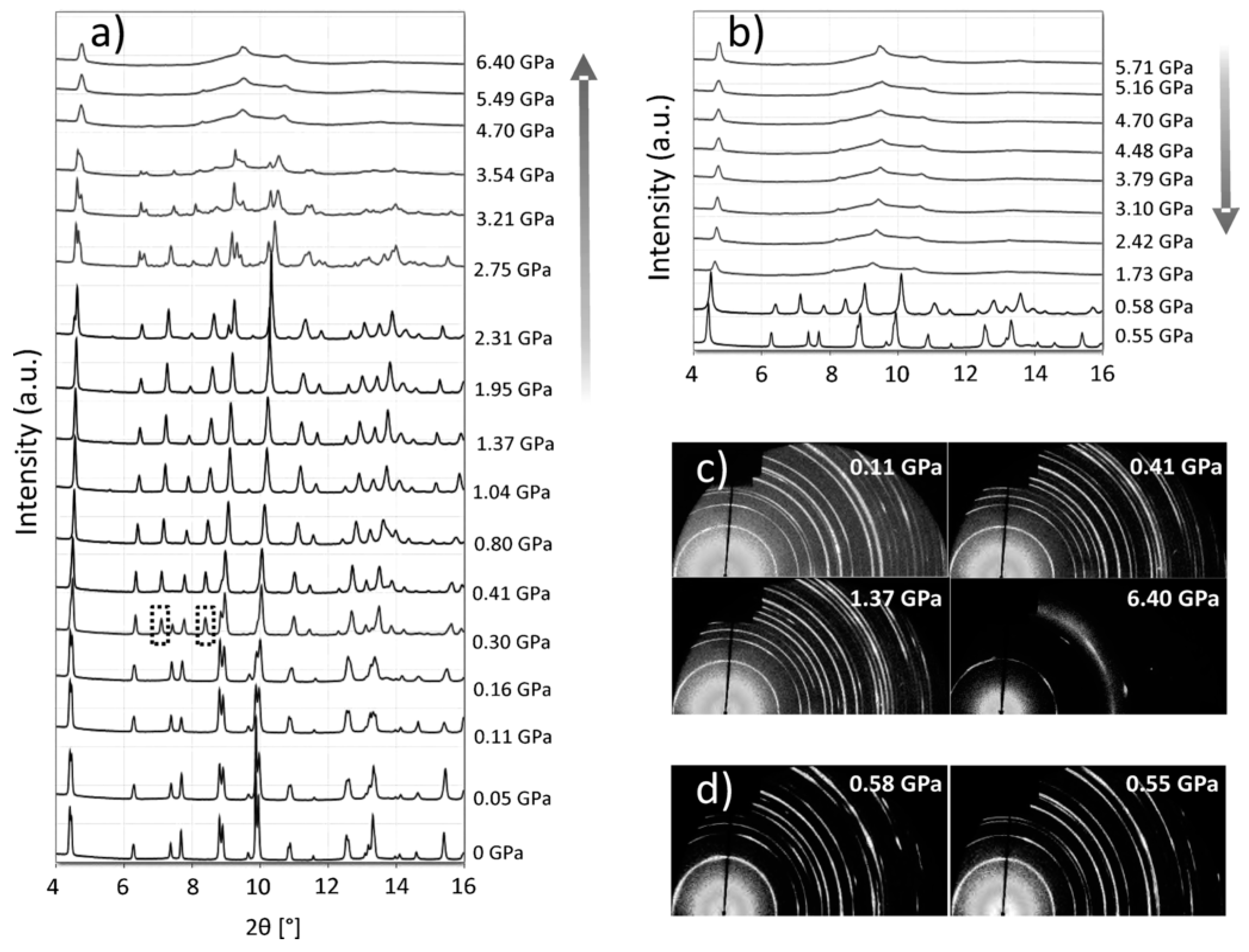
- Jiang, S.; Fang, Y.; Li, R.; Xiao, H.; Crowley, J.; Wang, C.; White, T.J.; Goddard, W.A.; Wang, Z.; Baikie, T.; et al. Pressure-dependent polymorphism and band-gap tuning of methylammonium Lead Iodide perovskite. Angew. Chem. Int. Ed. 2016, 55, 6540–6544. [Google Scholar] [CrossRef] [PubMed]
- Yamamuro, N.O.; Yamamuro, O.; Matsuo, T.; Suga, H. p-T phase relations of CH3NH3PbX3 (X = Cl, Br, I) crystals. J. Phys. Chem. Solids 1992, 53, 277–281. [Google Scholar] [CrossRef]
- Pisoni, A.; Jacimovic, J.; Barisic, O.S.; Spina, M.; Gaal, R.; Forro, L.; Horvath, E. Ultra-low thermal conductivity in organic–inorganic hybrid perovskite CH3NH3PbI3. J. Phys. Chem. Lett. 2014, 5, 2488–2492. [Google Scholar] [CrossRef] [PubMed]
- Qian, X.; Gu, X.; Yang, R. Lattice thermal conductivity of organic-inorganic hybrid perovskite CH3NH3PbI3. Appl. Phys. Lett. 2016, 108, 063902. [Google Scholar] [CrossRef]
- Ye, T.; Wang, X.; Li, X.; Yan, A.Q.; Ramakrishna, S.; Xu, J. Ultra-high Seebeck coefficient and low thermal conductivity of a centimeter-sized perovskite single crystal acquired by a modified fast growth method. J. Mater. Chem. C 2017, 5, 1255–1260. [Google Scholar] [CrossRef]
- Brunetti, B.; Cavallo, C.; Ciccioli, A.; Gigli, G.; Latini, A. On the thermal and thermodynamic (in)stability of methylammonium lead halide perovskites. Sci. Rep. 2016, 6, 31896. [Google Scholar] [CrossRef] [PubMed]
- Wang, Z.; Shi, Z.; Li, T.; Chen, Y.; Huang, W. Stability of PSCs: A prospective on the substitution of the A cation and X anion. Angew. Chem. Int. Ed. 2017, 56, 1190–1212. [Google Scholar] [CrossRef] [PubMed]
- Yang, J.; Siempelkamp, B.D.; Liu, D.; Kelly, T.L. Investigation of CH3NH3PbI3 degradation rates and mechanisms in controlled humidity environments using in situ techniques. ACS Nano 2015, 9, 1955–1963. [Google Scholar] [CrossRef] [PubMed]
- Han, Y.; Meyer, S.; Dkhissi, Y.; Weber, K.; Pringle, J.M.; Bach, U.; Spiccia, L.; Cheng, Y. Degradation observations of encapsulated planar CH3NH3PbI3 PSCs at high temperatures and humidity. J. Mater. Chem. A 2015, 3, 8139–8147. [Google Scholar] [CrossRef]
- Gangishetty, M.K.; Scott, R.W.J.; Kelly, T.L. Effect of relative humidity on crystal growth, device performance and hysteresis in planar heterojunction PSCs. Nanoscale 2016, 8, 6300–6307. [Google Scholar] [CrossRef] [PubMed]
- Cronin, H.M.; Jayawardena, K.D.G.I.; Stoeva, Z.; Shkunov, M.; Silva, S.R.P. Effects of ambient humidity on the optimum annealing time of mixed-halide PSCs. Nanotechnology 2017, 28, 114004. [Google Scholar] [CrossRef] [PubMed]
- Zhou, H.; Chen, Q.; Li, G.; Luo, S.; Song, T.B.; Duan, H.S.; Hong, Z.; You, J.; Liu, Y.; Yang, Y. Photovoltaics. Interface engineering of highly efficient PSCs. Science 2014, 345, 542–546. [Google Scholar] [CrossRef] [PubMed]
- Ito, S.; Tanaka, S.; Manabe, K.; Nishino, H. Effects of surface blocking layer of Sb2S3 on nanocrystalline TiO2 for CH3NH3PbI3 PSCs. J. Phys. Chem. C 2014, 118, 16995–17000. [Google Scholar] [CrossRef]
- Lee, S.W.; Kim, S.; Bae, S.; Cho, K.; Chung, T.; Mundt, L.E.; Lee, S.; Park, S.; Park, H.; Schubert, M.C.; et al. UV degradation and recovery of PSCs. Sci. Rep. 2016, 6, 38150. [Google Scholar] [CrossRef] [PubMed]
- Rafiee, J.; Mi, X.; Gullapalli, H.; Thomas, A.V.; Yavari, F.; Shi, Y.; Ajayan, P.M.; Koratkar, N.A. Wetting transparency of graphene. Nat. Mater. 2012, 11, 217–222. [Google Scholar] [CrossRef] [PubMed]
- Lim, E.L.; Yap, C.C.; Jumali, M.H.H.; Teridi, M.A.M.; Teh, C.H. A mini review: can graphene be a novel material for perovskite solar cell applications? Nano-Micro Lett. 2018, 10, 27. [Google Scholar] [CrossRef]
- Agresti, A.; Pescetelli, S.; Taheri, B.; Del Rio Castillo, A.E.; Cina, L.; Bonaccorso, F.; Di Carlo, A. Graphene-perovskite solar cells exceed 18% efficiency: a stability study. Chemsuschem 2016, 9, 2609–2619. [Google Scholar] [CrossRef] [PubMed]
- Bi, E.; Chen, H.; Xie, F.; Wu, Y.; Chen, W.; Su, Y.; Islam, A.; Grätzel, M.; Yang, X.; Han, L. Diffusion engineering of ions and charge carriers for stable efficient perovskite solar cells. Nat. Commun. 2017, 8, 15330. [Google Scholar] [CrossRef] [PubMed]
- Wang, Y.; Wang, S.; Chen, X.; Li, Z.; Wang, J.; Li, T.; Deng, X. Largely enhanced Voc and stability in perovskite solar cells with modified energy match by couple 2D interlayers. J. Mater. Chem. A 2018, 6, 4860–4867. [Google Scholar] [CrossRef]
- Chen, T.P.; Lin, C.W.; Li, S.S.; Tsai, Y.H.; Wen, C.Y.; Lin, W.J.; Hsiao, F.M.; Chiu, Y.P.; Tsukagoshi, K.; Osada, M.; Sasaki, T.; Chen, C.W. Self-assembly atomic stacking transport layer of 2D layered titania for perovskite solar cells with extended UV stability. Adv. Energy Mater. 2017, 8, 1701722. [Google Scholar] [CrossRef]
- Fang, Y.; Wang, X.; Wang, Q.; Huang, J.; Wu, T. Impact of annealing on spiro-OMeTAD and corresponding solid-state dye sensitized solar cells. Phys. Status Solidi 2014, 211, 2809. [Google Scholar] [CrossRef]
- Li, X.; Cai, M.; Zhou, Z.; Yun, K.; Xie, F.; Lan, Z.; Hua, J.; Han, L. A comparative study of o,p-dimethoxyphenyl-based hole transport materials by altering π-linker units for highly efficient and stable PSCs. J. Mater. Chem. A 2017, 5, 10480–10485. [Google Scholar] [CrossRef]
- Aitola, K.; Domanski, K.; Correa-Baena, J.-P.; Sveinbjörnsson, K.; Saliba, M.; Abate, A.; Grätzel, M.; Kauppinen, E.; Johansson, E.M.J.; Tress, W.; et al. High temperature-stable PSC based on low-cost carbon nanotube hole contact. Adv. Mater. 2017, 29, 1606398. [Google Scholar] [CrossRef] [PubMed]
- Zhang, M.; Lyu, M.; Yu, H.; Yun, J.H.; Wang, Q.; Wang, L. Stable and low-cost mesoscopic CH3NH3PbI2Br PSCs by using a thin Poly(3-hexylthiophene) layer as a hole transporter. Chem. Eur. J. 2015, 21, 434–439. [Google Scholar] [CrossRef] [PubMed]
- Arora, N.; Dar, M.I.; Hinderhofer, A.; Pellet, N.; Schreiber, F.; Zakeeruddin, S.M.; Grätzel, M. PSCs with CuSCN hole extraction layers yield stabilized efficiencies greater than 20%. Science 2017, 358, 768–771. [Google Scholar] [CrossRef] [PubMed]
- Snaith, H.J.; Abate, A.; Ball, J.M.; Eperon, G.E.; Leijtens, T.; Noel, N.K.; Stranks, S.D.; Wang, J.T.W.; Wojciechowski, K.; Zhang, W. Anomalous Hysteresis in PSCs. J. Phys. Chem. Lett. 2014, 5, 1511–1515. [Google Scholar] [CrossRef] [PubMed]
- Nemnes, G.A.; Besleaga, C.; Stancu, V.; Dogaru, D.E.; Leonat, L.N.; Pintilie, L.; Torfason, K.; Ilkov, M.; Manolescu, A.; Pintilie, I. Normal and inverted hysteresis in perovskite solar cells. J. Phys. Chem. C 2017, 121, 11207–11214. [Google Scholar] [CrossRef]
- Kegelmann, L.; Wolff, C.M.; Awino, C.; Lang, F.; Unger, E.L.; Korte, L.; Dittrich, T.; Neher, D.; Rech, B.; Albrecht, S. It takes two to tango—Double-layer selective contacts in PSCs for improved device performance and reduced hysteresis. ACS Appl. Mater. Interfaces 2017, 9, 17245–17255. [Google Scholar] [CrossRef] [PubMed]
- Guo, Y.; Liu, T.; Wang, N.; Luo, Q.; Lin, H.; Li, J.; Jiang, Q.; Wu, L.; Guo, Z. Ni-doped α-Fe2O3 as electron transporting material for planar heterojunction PSCs with improved efficiency, reduced hysteresis and ultraviolet stability. Nano Energy 2017, 38, 193–200. [Google Scholar] [CrossRef]
- Chen, H.W.; Sakai, N.; Ikegami, M.; Miyasaka, T. Emergence of hysteresis and transient ferroelectric response in organo-lead halide PSCs. J. Phys. Chem. Lett. 2015, 6, 164–169. [Google Scholar] [CrossRef] [PubMed]
- Azpiroz, J.M.; Mosconi, E.; Bisquert, J.; De Angelis, F. Defect migration in methylammonium lead iodide and its role in PSC operation. Energy Environ. Sci. 2015, 8, 2118–2127. [Google Scholar] [CrossRef]
- Van Reenen, S.; Kemerink, M.; Snaith, H.J. Modeling anomalous hysteresis in PSCs. J. Phys. Chem. Lett. 2015, 6, 3808–3814. [Google Scholar] [CrossRef] [PubMed]
- Almora, O.; Zarazua, I.; Mas-Marza, E.; Mora-Sero, I.; Bisquert, J.; Belmonte, G.G. Capacitive dark currents, hysteresis and electrode polarization in lead halide PSCs. J. Phys. Chem. Lett. 2015, 6, 1645–1652. [Google Scholar] [CrossRef] [PubMed]
- Elumalai, N.K.; Uddin, A. Hysteresis in organic-inorganic hybrid PSCs. Sol. Energy Mater Sol. Cells 2016, 157, 476–509. [Google Scholar] [CrossRef]
- Chen, B.; Yang, M.; Priya, S.; Zhu, K. Origin of J-V hysteresis in PSCs. J. Phys. Chem. Lett. 2016, 7, 905–917. [Google Scholar] [CrossRef] [PubMed]
- Li, C.; Guerrero, A.; Zhong, Y.; Huettner, S. Origins and mechanisms of hysteresis in organometal halide perovskites. J. Phys. Condens. Matter 2017, 29, 193001. [Google Scholar] [CrossRef] [PubMed]
- Domanski, K.; Alharbi, E.A.; Hagfeldt, A.; Grätzel, M.; Tress, W. Systematic investigation of the impact of operation conditions on the degradation behavior of perovskite solar cells. Nat. Energy 2018, 3, 61–67. [Google Scholar] [CrossRef]
- Christians, J.A.; Manser, J.S.; Kamat, P.V. Best practices in PSC efficiency measurements. Avoiding the error of making bad cells look good. J. Phys. Chem. Lett. 2015, 6, 852–857. [Google Scholar] [CrossRef] [PubMed]
- Fabini, D. Quantifying the potential for lead pollution from halide perovskite photovoltaics. J. Phys. Chem. Lett. 2015, 6, 3546–3548. [Google Scholar] [CrossRef] [PubMed]
- Chen, P.; Qi, J.; Klug, M.T.; Dang, X.; Hammond, P.T.; Belcher, A.M. Environmentally responsible fabrication of efficient PSCs from recycled car batteries. Energy Environ. Sci. 2014, 7, 3659. [Google Scholar] [CrossRef]
- Noel, N.K.; Stranks, S.D.; Abate, A.; Wehrenfennig, C.; Guarnera, S.; Hagighirad, A.A.; Sadhanala, A.; Eperon, G.E.; Pathak, S.K.; Johnston, M.B.; et al. Lead-free organic–inorganic tin halide perovskites for photovoltaic applications. Energy Environ. Sci. 2014, 7, 3061–3068. [Google Scholar] [CrossRef]
- Hoshi, H.; Shigeeda, N.; Dai, T. Improved oxidation stability of tin iodide cubic perovskite treated by 5-ammonium valeric acid iodide. Mater. Lett. 2016, 183, 391–393. [Google Scholar] [CrossRef]
- Lee, S.J.; Shin, S.S.; Kim, Y.C.; Kim, D.; Ahn, T.K.; Noh, J.H.; Seo, J.; Seok, S.I. Fabrication of efficient formamidinium Tin Iodide PSCs through SnF2–Pyrazine complex. J. Am. Chem. Soc. 2016, 138, 3974–3977. [Google Scholar] [CrossRef] [PubMed]
- Zhu, H.L.; Xiao, J.; Mao, J.; Zhang, H.; Zhao, Y.; Choy, W.C.H. Controllable crystallization of CH3NH3Sn0.25Pb0.75I3 perovskites for hysteresis-free solar cells with efficiency reaching 15.2%. Adv. Funct. Mater. 2017, 27, 1605469. [Google Scholar] [CrossRef]
- Im, J.; Stoumpos, C.C.; Jin, H.; Freeman, A.J.; Kanatzidis, M.G. Antagonism between spin–orbit coupling and steric effects causes anomalous band gap evolution in the perovskite photovoltaic materials CH3NH3Sn1–xPbxI3. J. Phys. Chem. Lett. 2015, 6, 3503–3509. [Google Scholar] [CrossRef] [PubMed]
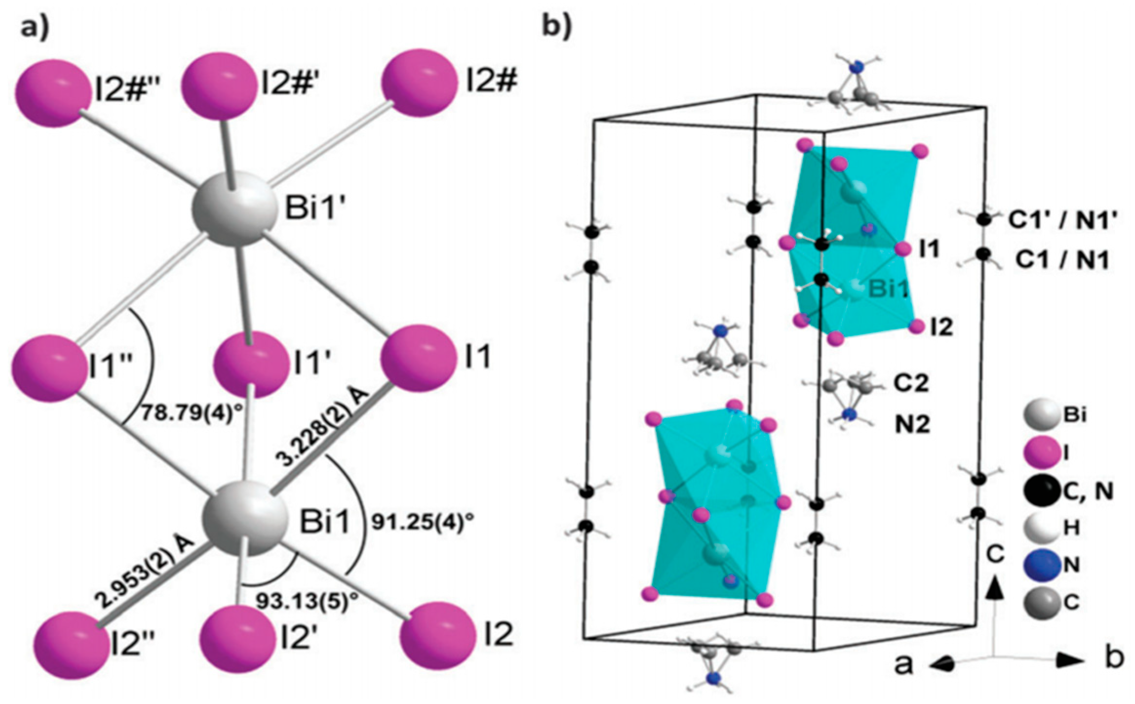
- Eckhardt, K.; Bon, V.; Getzschmann, J.; Grothe, J.; Wisser, F.M.; Kaskel, S. Crystallographic insights into (CH3NH3)3(Bi2I9): A new lead-free hybrid organic–inorganic material as a potential absorber for photovoltaics. Chem. Commun. 2016, 52, 3058–3060. [Google Scholar] [CrossRef] [PubMed]
- Hoye, R.L.Z.; Brandt, R.E.; Osherov, A.; Stevanovic, V.; Stranks, S.D.; Wilson, M.W.B.; Kim, H.; Akey, A.J.; Perkins, J.D.; Kurchin, R.C.; et al. Methylammonium Bismuth Iodide as a Lead-free, stable hybrid organic–inorganic solar absorber. Chem. Eur. J. 2016, 22, 2605–2610. [Google Scholar] [CrossRef] [PubMed]
- Park, B.W.; Phillippe, B.; Zhang, X.; Rensmo, H.; Boschloo, G.; Johansson, E.M.J. Bismuth based hybrid perovskites A3Bi2I9 (A: Methylammonium or Cesium) for solar cell application. Adv. Mater. 2015, 27, 6806–6813. [Google Scholar] [CrossRef] [PubMed]
- Zhang, X.; Wu, G.; Gu, Z.; Guo, B.; Liu, W.; Yang, S.; Ye, T.; Chen, C.; Tu, W.; Chen, H. Active-layer evolution and efficiency improvement of (CH3NH3)3Bi2I9-based solar cell on TiO2-deposited ITO substrate. Nano Res. 2016, 9, 2921–2930. [Google Scholar] [CrossRef]
- Lehner, A.J.; Fabini, D.H.; Evans, H.A.; Hebert, C.A.; Smock, S.R.; Hu, J.; Wang, H.; Zwanziger, J.W.; Chabinyc, M.L.; Seshadri, R. Crystal and electronic structures of complex Bismuth Iodides A3Bi2I9 (A = K, Rb, Cs) related to perovskite: Aiding the rational design of photovoltaics. Chem. Mater. 2015, 27, 7137–7148. [Google Scholar] [CrossRef]
- Scholz, M.; Flender, O.; Oum, K.; Lenzer, T. Pronounced exciton dynamics in the vacancy-ordered Bismuth halide perovskite (CH3NH3)3Bi2I9 observed by ultrafast UV-Vis-NIR transient absorption spectroscopy. J. Phys. Chem. C 2017, 121, 12110–12116. [Google Scholar] [CrossRef]
- Slavney, A.H.; Hu, T.; Lindenberg, A.M.; Karunadasa, H.I. A Bismuth-halide double perovskite with long carrier recombination lifetime for photovoltaic applications. J. Am. Chem. Soc. 2016, 138, 2138–2141. [Google Scholar] [CrossRef] [PubMed]
- Wei, F.; Deng, Z.; Sun, S.; Xie, F.; Kieslich, G.; Evans, D.M.; Carpenter, M.A.; Bristowe, P.D.; Cheetham, A.K. The synthesis, structure and electronic properties of a lead-free hybrid inorganic-organic double perovskite (MA)2KBiCl6 (MA = methylammonium). Mater. Horizons 2016, 3, 328–332. [Google Scholar] [CrossRef]
- Ming, W.; Shi, H.; Du, M. Large dielectric constant, high acceptor density and deep electron traps in PSC material CsGeI3. J. Mater. Chem. A 2016, 4, 13852–13858. [Google Scholar] [CrossRef]
- Lu, X.; Zhao, Z.; Li, K.; Han, Z.; Wei, S.; Guo, C.; Zhou, S.; Wu, Z.; Guo, W.; Wu, C.L. First-principles insight into the photoelectronic properties of Ge-based perovskites. RSC Adv. 2016, 6, 86976–86981. [Google Scholar] [CrossRef]
- Jacobsson, T.J.; Pazoki, M.; Hagfeldt, A.; Edvinsson, T. Goldschmidt’s rules and strontium replacement in lead halogen PSCs: Theory and preliminary experiments on CH3NH3SrI3. J. Phys. Chem. C 2015, 119, 25673–25683. [Google Scholar] [CrossRef]
- Uribe, J.I.; Ramirez, D.; Osorio-Guillen, J.M.; Osorio, J.; Jaramillo, F. CH3NH3CaI3 perovskite: Synthesis, characterization and first-principles studies. J. Phys. Chem. C 2016, 120, 16393–16398. [Google Scholar] [CrossRef]
- Dai, X.; Zhang, Y.; Shen, H.; Luo, Q.; Zhao, X.; Li, J.; Lin, H. Working from Both Sides: Composite Metallic Semitransparent Top Electrode for High Performance Perovskite Solar Cells. ACS Appl. Mater. Interfaces 2016, 8, 4523–4531. [Google Scholar] [CrossRef] [PubMed]


| ETM | HTM | Jsc (mA/cm2) | Voc (V) | FF | η (%) | Ref. |
|---|---|---|---|---|---|---|
| c-TiO2/mp-TiO2 (spray pyrolysis) | spiro-MeOTAD | 22.3 | 1.06 | 0.77 | 18.1 | [99] |
| CuSCN | 21.8 | 1.1 | 0.692 | 16.6 | [100] | |
| FDT | 22.7 | 1.15 | 0.76 | 20.2 | [101] | |
| PTAA | 20.7 | 1.05 | 0.74 | 16.1 | [102] | |
| TiO2 (spray pyrolysis) | CuGaO2 | 21.66 | 1.11 | 0.77 | 18.51 | [103] |
| TiO2 (spray pyrolysis) | PTAA | 20.1 | 1.1 | 0.78 | 17.2 | [104] |
| TiO2 | spiro-MeOTAD | 21.5 | 1.07 | 0.67 | 15.4 | [105] |
| TiO2 | P3HT | 19.1 | 0.98 | 0.66 | 12.4 | [106] |
| TiO2 (with screen printing, C60 treatment) | spiro-MeOTAD | 19.6 | 0.84 | 0.72 | 11.7 | [98] |
| TiO2 (ALD) | Carbon | 19.53 | 0.965 | 0.4147 | 7.82 | [107] |
| TiO2 (ALD)/PCBM | NiOx | 19.7 | 0.93 | 0.477 | 8.8 | [108] |
| TiO2 (sputtering) | PTAA | 20.77 | 1.108 | 0.69 | 15.88 | [109] |
| ZrO2/TiO2 | spiro-MeOTAD | 22.20 | 1.05 | 0.8 | 17.88 | [110] |
| TiO2/BaTiO3 (TiCl4-treated) | spiro-MeOTAD | 19.3 | 0.962 | 0.67 | 12.4 | [111] |
| ZnO | spiro-MeOTAD | 20.5 | 1.03 | 0.748 | 15.7 | [11] |
| ZnO | P3HT | 14.94 | 0.9329 | 0.6267 | 8.77 | [112] |
| SnO2 | spiro-OMeTAD | 21.65 | 1.06 | 0.659 | 15.13 | [96] |
| Nb-SnO2 | 22.36 | 1.08 | 0.727 | 17.57 | ||
| La-BaSnO3 | PTAA | 23.4 | 1.12 | 0.813 | 21.3 | [17] |
| PCBM (vacuum evaporation) | NiO (sputtering) | 19.8 | 0.96 | 0.61 | 11.6 | [113] |
| PCBM | NiO | 18.74 | 1.04 | 0.689 | 13.43 | [114] |
| NiO (sputtering) | 20.33 | 1.08 | 0.69 | 15.15 | [115] | |
| PEDOT: PSS | 18.9 | 0.972 | 0.8016 | 15.32 | [116] | |
| C60 (vacuum evaporation) | PTAA | 22.96 | 1.11 | N/A | 19.5 | [117] |
| TiO2/r-GO | Spiro-OMeTAD | 22.0 | 0.93 | 0.707 | 14.5 | [118] |
| Phase | Temperature (K) | Crystal System | Space Group | Lattice (pm) | Volume (104 pm3) |
|---|---|---|---|---|---|
| CH3NH3PbCl3- | |||||
| α | >178.8 | cubic | Pm3m | a = 567.5 | 182.8 |
| β | 172.9–178.8 | tetragonal | P4/mmm | a = 565.6 | 180.1 |
| c = 563.0 | |||||
| γ | <172.9 | orthorhombic | P2221 | a = 567.3 | 357.0 |
| b = 562.8 | |||||
| c = 1118.2 | |||||
| CH3NH3PbBr3- | |||||
| α | >236.9 | cubic | Pm3m | a = 590.1(1) | 206.3 (260 K) |
| β | 155.1–236.9 | tetragonal | I4/mcm | a = 832.2(2) | 819.4 |
| c = 1183.2(7) | |||||
| γ | 149.5–155.1 | tetragonal | P4/mcm | a = 589.4(2) | |
| c = 586.1(2) | |||||
| δ | <149.5 | orthorhombic | Pna21 | a = 797.9(1) | 811.1 |
| b = 858.0(2) | |||||
| c = 1184.9(2) | |||||
| CH3NH3PbI3- | |||||
| α | >327.4 | cubic | Pm3m | a = 632.85(4) | 253.5 |
| β | 162.2–327.4 | tetragonal | I4/mcm | a = 885.5(6) | 992.6 |
| c = 1265.9(8) | |||||
| γ | <162.2 | orthorhombic | Pna21 | a = 886.1(2) | 959.5 |
| b = 858.1(2) | |||||
| c = 1262.0(3) |
© 2018 by the authors. Licensee MDPI, Basel, Switzerland. This article is an open access article distributed under the terms and conditions of the Creative Commons Attribution (CC BY) license (http://creativecommons.org/licenses/by/4.0/).
Share and Cite
Shi, Z.; Jayatissa, A.H. Perovskites-Based Solar Cells: A Review of Recent Progress, Materials and Processing Methods. Materials 2018, 11, 729. https://doi.org/10.3390/ma11050729
Shi Z, Jayatissa AH. Perovskites-Based Solar Cells: A Review of Recent Progress, Materials and Processing Methods. Materials. 2018; 11(5):729. https://doi.org/10.3390/ma11050729
Chicago/Turabian StyleShi, Zhengqi, and Ahalapitiya H. Jayatissa. 2018. "Perovskites-Based Solar Cells: A Review of Recent Progress, Materials and Processing Methods" Materials 11, no. 5: 729. https://doi.org/10.3390/ma11050729
APA StyleShi, Z., & Jayatissa, A. H. (2018). Perovskites-Based Solar Cells: A Review of Recent Progress, Materials and Processing Methods. Materials, 11(5), 729. https://doi.org/10.3390/ma11050729