Improvements on the Interfacial Properties of High-k/Ge MIS Structures by Inserting a La2O3 Passivation Layer


Abstract
:1. Introduction
2. Experimental Section
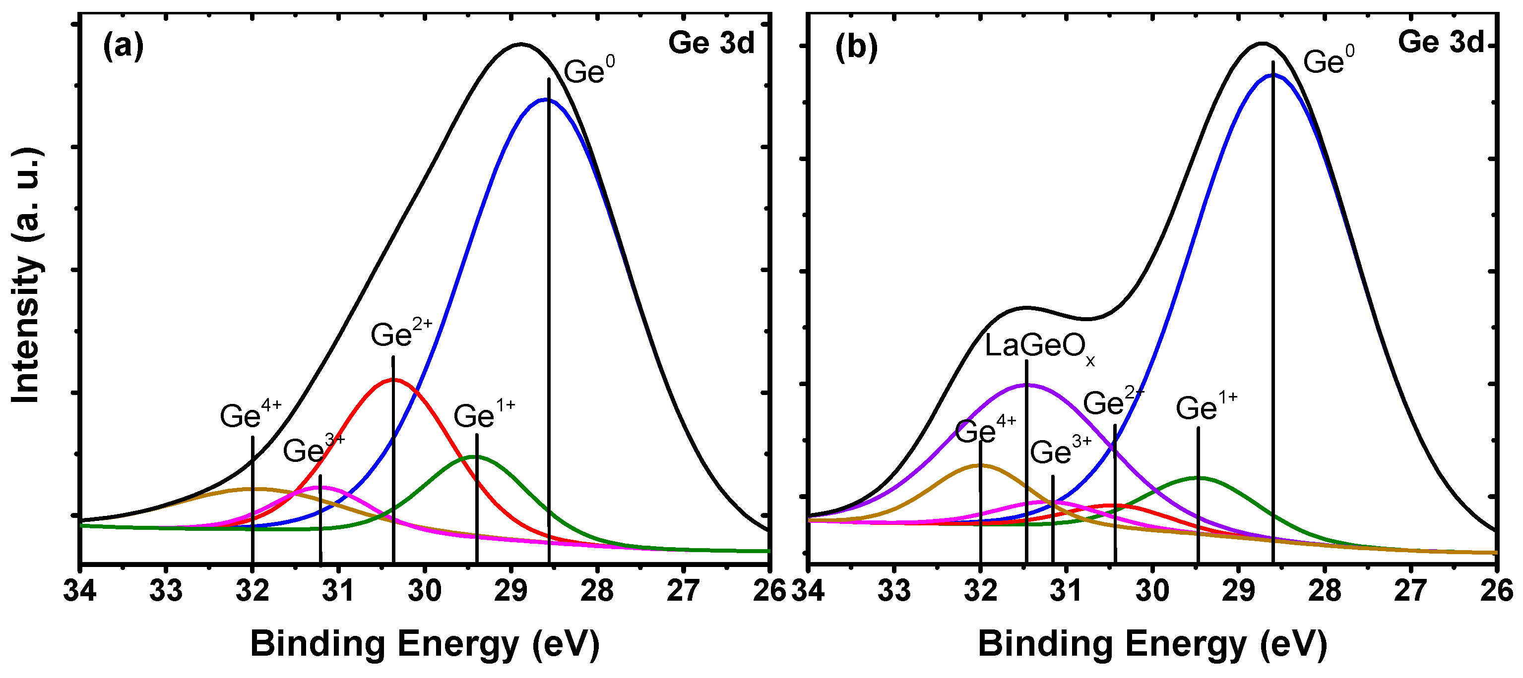
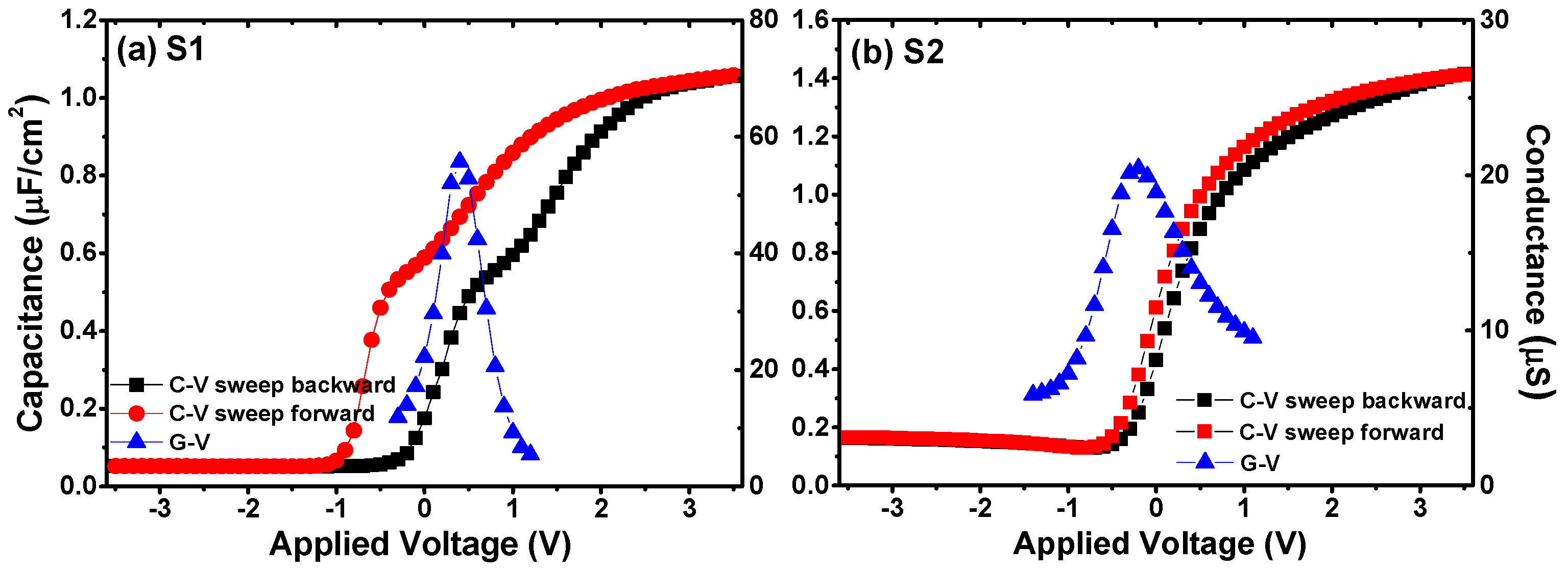
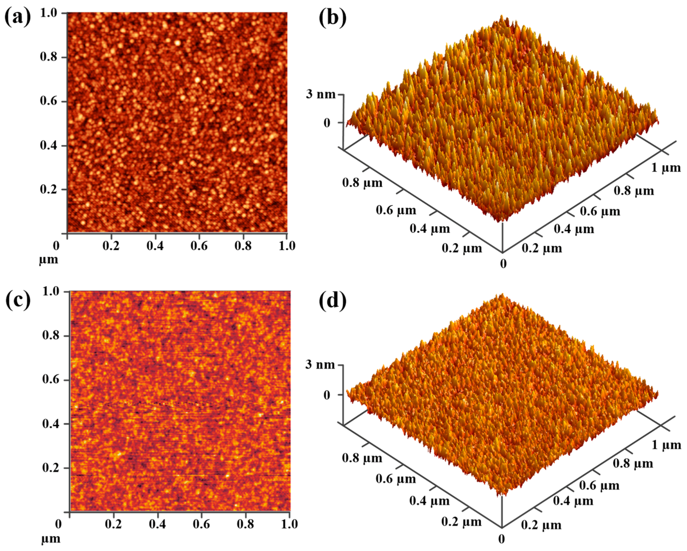
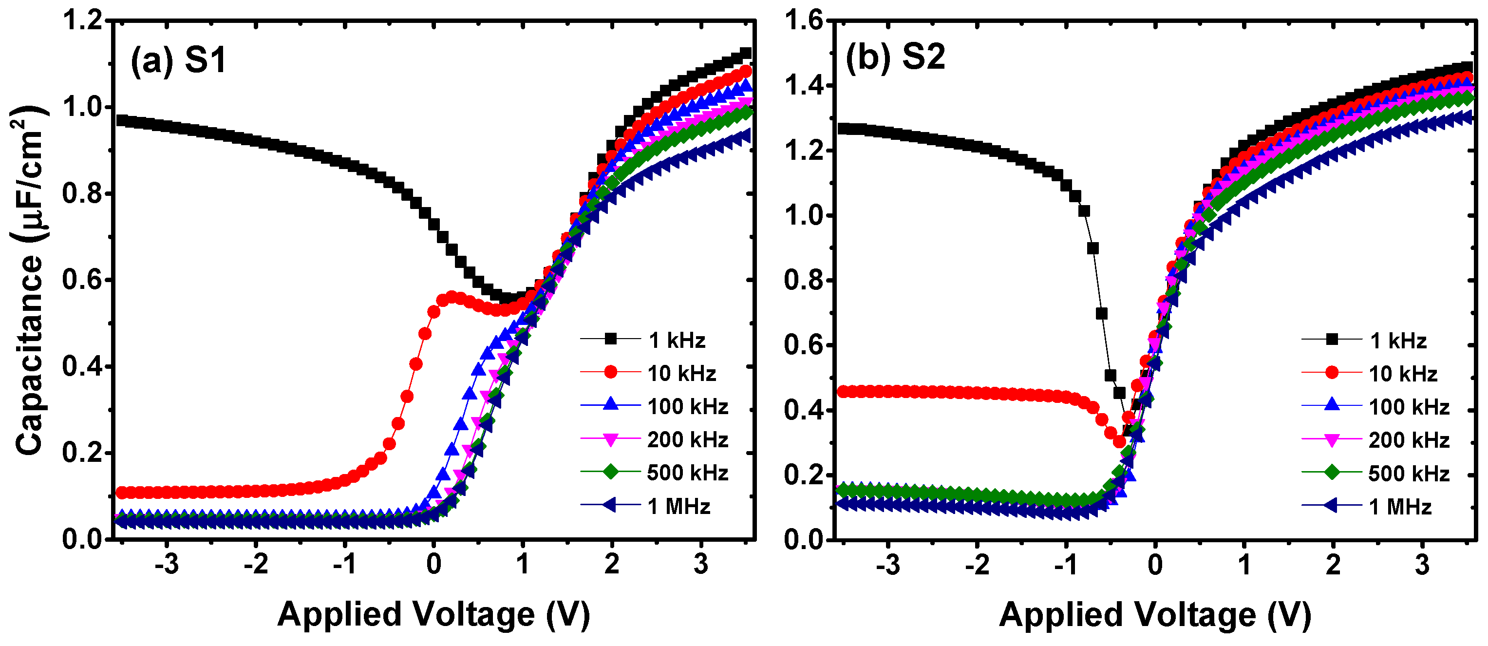
3. Results and Discussion
4. Conclusions
Author Contributions
Funding
Conflicts of Interest
References
- Wilk, G.D.; Wallace, R.M.; Anthony, J.M. High-k gate dielectrics: Current status and materials properties considerations. J. Appl. Phys. 2001, 89, 10. [Google Scholar] [CrossRef]
- Lee, B.H.; Oh, J.; Tseng, H.H.; Jammy, R.; Huff, H. Gate stack technology for nanoscale devices. Mater. Today 2006, 9, 32–40. [Google Scholar] [CrossRef]
- Kingon, A.I.; Maria, J.P.; Streiffer, S.K. Alternative dielectrics to silicon dioxide for memory and logic devices. Nature 2000, 406, 1032. [Google Scholar] [CrossRef] [PubMed]
- Dey, S.; Tapily, K.; Consiglio, S.; Clark, R.D.; Wajda, C.S.; Leusink, G.J.; Woll, A.R.; Diebold, A.C. Role of Ge and Si substrates in higher-k tetragonal phase formation and interfacial properties in cyclical atomic layer deposition-anneal Hf1−xZrxO2/Al2O3 thin film stacks. J. Appl. Phys. 2016, 120, 125304. [Google Scholar] [CrossRef]
- Simoen, E.; Mitard, J.; Hellings, G.; Eneman, G.; DeJaeger, B.; Witters, L.; Vincent, B.; Loo, R.; Delabie, A.; Sioncke, S.; et al. Challenges and opportunities in advanced Ge pMOSFETs. Mat. Sci. Semicond. Process. 2012, 15, 588–600. [Google Scholar] [CrossRef]
- Yi, S.H.; Chang-Liao, K.S.; Wu, T.Y.; Hsu, C.W.; Huang, J.Y. High performance Ge pMOSFETs with HfO2/Hf-Cap/GeOx gate stack and suitable post metal annealing treatments. IEEE Electron Device Lett. 2017, 38, 544–547. [Google Scholar] [CrossRef]
- Xie, Q.; Deng, S.; Schaekers, M.; Lin, D.; Caymax, M.; Delabie, A.; Qu, X.P.; Jiang, Y.L.; Deduytsche, D.; Detavernier, C. Germanium surface passivation and atomic layer deposition of high-k dielectrics—A tutorial review on Ge-based MOS capacitors. Semicond. Sci. Technol. 2012, 27, 074012. [Google Scholar] [CrossRef]
- Kamata, Y. High-k/Ge MOSFETs for future nanoelectronics. Mater. Today 2008, 11, 30–38. [Google Scholar] [CrossRef]
- Houssa, M.; Chagarov, E.; Kummel, A. Surface defects and passivation of Ge and III–V interfaces. MRS Bull. 2009, 34, 504–513. [Google Scholar] [CrossRef]
- Seok, T.J.; Cho, Y.J.; Jin, H.S.; Kim, D.H.; Kim, D.W.; Lee, S.M.; Park, J.B.; Won, J.Y.; Kim, S.K.; Hwang, C.S.; et al. High quality interfacial sulfur passivation via H2S pre-deposition annealing for an atomic-layer-deposited HfO2 film on a Ge substrate. J. Mater. Chem. C 2016, 4, 850–856. [Google Scholar] [CrossRef]
- Yoshida, T.; Kato, K.; Shibayama, S.; Sakashita, M.; Taoka, N.; Takeuchi, W.; Nakatsuka, O.; Zaima, S. Interface properties of Al2O3/Ge structures with thin Ge oxide interfacial layer formed by pulsed metal organic chemical vapor deposition. Jpn J. Appl. Phys. 2014, 53, 8S1. [Google Scholar] [CrossRef]
- Bethge, O.; Henkel, C.; Abermann, S.; Pozzovivo, G.; Stoeger-Pollach, M.; Werner, W.S.M.; Smoliner, J.; Bertagnolli, E. Stability of La2O3 and GeO2 passivated Ge surfaces during ALD of ZrO2 high-k dielectric. Appl. Surf. Sci. 2012, 258, 3444–3449. [Google Scholar] [CrossRef]
- Seo, Y.; Lee, T.I.; Chang, M.Y.; Park, B.E.; Wan, S.H.; Kim, H.J.; Yu, H.Y.; Cho, B.J. The impact of an ultrathin Y2O3 layer on GeO2 passivation in Ge MOS gate stacks. IEEE T. Electron. Dev. 2017, 64, 3303–3307. [Google Scholar] [CrossRef]
- Kouda, M.; Suzuki, T.; Kakushima, K.; Ahmet, P.; Iwai, H.; Yasuda, T. Electrical properties of CeO2/La2O3 stacked gate dielectrics fabricated by chemical vapor deposition and atomic layer deposition. Jpn J. Appl. Phys. 2012, 51, 121101. [Google Scholar]
- Lin, C.C.; Wu, Y.H.; Wu, C.Y.; Lee, C.W. Surface passivation of Ge MOS devices by SmGeOx with sub-nm EOT. IEEE Electron Device Lett. 2014, 35, 3. [Google Scholar] [CrossRef]
- Houssa, M.; Pourtois, G.; Caymax, M.; Meuris, M.; Heyns, M.M. First-principles study of the structural and electronic properties of interfaces (M=Al, La, or Hf). Appl. Phys. Lett. 2008, 92, 242101. [Google Scholar] [CrossRef]
- Liu, Q.Y.; Fang, Z.B.; Liu, S.Y.; Tan, Y.S.; Chen, J.J. Band offsets of La2O3 films on Ge substrates grown by radio frequency magnetron sputtering. Mater. Lett. 2014, 116, 43–45. [Google Scholar] [CrossRef]
- Abermann, S.; Bethge, O.; Henkel, C.; Bertagnolli, E. Atomic layer deposition of ZrO2/La2O3 high-k dielectrics on germanium reaching 0.5 nm equivalent oxide thickness. Appl. Phys. Lett. 2009, 94, 262904. [Google Scholar] [CrossRef]
- Mitrovic, I.Z.; Althobaiti, M.; Weerakkody, A.D.; Dhanak, V.R.; Linhart, W.M.; Veal, T.D.; Sedghi, N.; Hall, S.; Chalker, P.R.; Tsoutsou, D. Ge interface engineering using ultra-thin La2O3 and Y2O3 films: A study into the effect of deposition temperature. J. Appl. Phys. 2014, 115, 114102. [Google Scholar] [CrossRef]
- Mavrou, G.; Galata, S.; Tsipas, P.; Sotiropoulos, A.; Panayiotatos, Y.; Dimoulas, A.; Evangelou, E.K.; Seo, J.W.; Dieker, C. Electrical properties of La2O3 and HfO2/La2O3 gate dielectrics for germanium metal-oxide-semiconductor devices. J. Appl. Phys. 2008, 103, 014506. [Google Scholar] [CrossRef]
- Schmeisser, D.; Schnell, R.D.; Bogen, A.; Himpsel, F.J.; Rieger, D.; Landgren, G.; Morar, J.F. Surface oxidation states of germanium. Surf. Sci. 1986, 172, 455–465. [Google Scholar] [CrossRef]
- Oh, I.K.; Kim, M.K.; Lee, J.S.; Lee, C.W.; Lansalot-Matras, C.; Noh, W.; Park, J.; Noori, A.; Thompson, D.; Chu, S.; et al. The effect of La2O3-incorporation in HfO2 dielectrics on Ge substrate by atomic layer deposition. Appl. Surf. Sci. 2013, 287, 349–354. [Google Scholar] [CrossRef]
- Molle, A.; Baldovino, S.; Fanciulli, M.; Tsoutsou, D.; Golias, E.; Dimoulas, A. Impact of post deposition annealing in the electrically active traps at the interface between Ge (001) substrates and LaGeOx films grown by molecular beam deposition. J. Appl. Phys. 2011, 110, 084504. [Google Scholar] [CrossRef]
- Henkel, C.; Abermann, S.; Bethge, O.; Pozzovivo, G.; Klang, P.; Reiche, M.; Bertagnolli, E. Ge p-MOSFETs with scaled ALD La2O3/ZrO2 gate dielectrics. IEEE Trans. Electron Devices 2010, 57, 3295–3302. [Google Scholar] [CrossRef]
- Bhaisare, M.; Misra, A.; Kottantharayil, A. Aluminum oxide deposited by pulsed-DC reactive sputtering for crystalline silicon surface passivation. IEEE J. Photovolt. 2013, 3, 930–935. [Google Scholar] [CrossRef]
- Cao, D.; Cheng, X.H.; Jia, T.T.; Xu, D.W.; Wang, Z.J.; Xia, C.; Yu, Y.H. Characterization of HfO2/La2O3 layered stacking deposited on Si substrate. J. Vac. Sci. Technol. B Nanotechnol. Microelectron. 2013, 31, 01A113. [Google Scholar] [CrossRef]
- Scarel, G.; Debernardi, A.; Tsoutsou, D.; Spiga, S.; Capelli, S.C.; Lamagna, L.; Volkos, S.N.; Alia, M.; Fanciulli, M. Vibrational and electrical properties of hexagonal La2O3 films. Appl. Phys. Lett. 2007, 91, 102901. [Google Scholar] [CrossRef]
- Pelloquin, S.; Saint-Girons, G.; Baboux, N.; Albertini, D.; Hourani, W.; Penuelas, J.; Grenet, G.; Plossu, C.; Hollinger, G. LaAlO3/Si capacitors: Comparison of different molecular beam deposition conditions and their impact on electrical properties. J. Appl. Phys. 2013, 113, 034106. [Google Scholar] [CrossRef]
- Kaya, S.; Yilmaz, E. Influences of Co-60 gamma-ray irradiation on electrical characteristics of Al2O3 MOS capacitors. J. Radioanal. Nucl. Chem. 2014, 302, 425–431. [Google Scholar] [CrossRef]
- Hauser, J.R.; Ahmed, K. Characterization of ultra-thin oxides using electrical C-V and I-V measurements. AIP Conf. Proc. 1998, 449, 235. [Google Scholar]
- Kumar, A.; Mondal, S.; Rao, K.S.R.K. Critical investigation of high performance spin-coated high-κ titania thin films based MOS capacitor. J. Mater. Sci. Mater. Electron. 2016, 27, 5264–5270. [Google Scholar] [CrossRef]
- Sze, S.M.; Ng, K.K. Physics of Semiconductor Devices, 3rd ed.; John Wiley & Sons: Hoboken, NJ, USA, 2006. [Google Scholar]
- Suzuki, T.; Kouda, M.; Ahmet, P.; Iwai, H.; Kakushima, K.; Yasuda, T. La2O3 gate insulators prepared by atomic layer deposition: Optimal growth conditions and MgO/La2O3 stacks for improved metal-oxide-semiconductor characteristics. J. Vac. Sci. Technol. A 2012, 30, 051507. [Google Scholar] [CrossRef]
- Hill, W.A.; Coleman, C.C. A single-frequency approximation for interface-state density determination. Solid State Electron. 1980, 23, 987. [Google Scholar] [CrossRef]
- Lei, C.; Wang, C.; Wang, G.; Sun, X.; Li, T.; Liu, L. Dielectric relaxations of LaAlO3 ceramics over broad temperature range. J. Alloy. Compd. 2013, 555, 51. [Google Scholar] [CrossRef]
- Kita, K.; Suzuki, S.; Nomura, H.; Takahashi, T.; Nishimura, T.; Toriumi, A. Direct evidence of GeO volatilization from GeO2/Ge and impact of its suppression on GeO2/Ge metal-insulator-semiconductor characteristics. Jpn J. Appl. Phys. 2008, 47, 2349–2353. [Google Scholar] [CrossRef]
- Spahr, H.; Bülow, T.; Nowak, C.; Hirschberg, F.; Reinker, J.; Hamwi, S.; Johannes, H.H.; Kowalsky, W. Impact of morphological defects on the electrical breakdown of ultra thin atomic layer deposition processed Al2O3 layers. Thin Solid Films 2013, 534, 172–176. [Google Scholar] [CrossRef]
- Jinesh, K.B.; Klootwijk, J.H.; Lamy, Y.; Wolters, R.; Tois, E.; Tuominen, M.; Roozeboom, F.; Besling, W.F.A. Enhanced electrical properties of atomic layer deposited La2O3 thin films with embedded ZrO2 nanocrystals. Appl. Phys. Lett. 2008, 93, 172904. [Google Scholar] [CrossRef]


| Sample | Cox (µF/cm2) | k | ΔVFB (mV) | Not (cm−2) | Dit (eV−1·cm−2) |
|---|---|---|---|---|---|
| S1 | 1.096 | 7.95 | 863 | 5.91 × 10¹² | 1.13 × 10¹³ |
| S2 | 1.438 | 11.10 | 174 | 1.56 × 10¹² | 4.97 × 10¹² |
© 2018 by the authors. Licensee MDPI, Basel, Switzerland. This article is an open access article distributed under the terms and conditions of the Creative Commons Attribution (CC BY) license (http://creativecommons.org/licenses/by/4.0/).
Share and Cite
Zhao, L.; Liu, H.; Wang, X.; Wang, Y.; Wang, S. Improvements on the Interfacial Properties of High-k/Ge MIS Structures by Inserting a La2O3 Passivation Layer. Materials 2018, 11, 2333. https://doi.org/10.3390/ma11112333
Zhao L, Liu H, Wang X, Wang Y, Wang S. Improvements on the Interfacial Properties of High-k/Ge MIS Structures by Inserting a La2O3 Passivation Layer. Materials. 2018; 11(11):2333. https://doi.org/10.3390/ma11112333
Chicago/Turabian StyleZhao, Lu, Hongxia Liu, Xing Wang, Yongte Wang, and Shulong Wang. 2018. "Improvements on the Interfacial Properties of High-k/Ge MIS Structures by Inserting a La2O3 Passivation Layer" Materials 11, no. 11: 2333. https://doi.org/10.3390/ma11112333
APA StyleZhao, L., Liu, H., Wang, X., Wang, Y., & Wang, S. (2018). Improvements on the Interfacial Properties of High-k/Ge MIS Structures by Inserting a La2O3 Passivation Layer. Materials, 11(11), 2333. https://doi.org/10.3390/ma11112333