Article

Miniature Spectroscopes with Two-Dimensional Guided-Mode Resonant Metal Grating Filters Integrated on a Photodiode Array

Department of Finemechanics, Tohoku University, Miyagi 980-8579, Japan
*
Author to whom correspondence should be addressed.
Materials 2018, 11(10), 1924; https://doi.org/10.3390/ma11101924
Submission received: 18 September 2018 / Revised: 3 October 2018 / Accepted: 5 October 2018 / Published: 10 October 2018
(This article belongs to the Special Issue New Horizon of Plasmonics and Metamaterials)

Abstract

:
A small spectroscope with 25 color sensors was fabricated by combining metamaterial color filters and Si photodiodes. The metamaterial color filters consisted of guided-mode resonant metal gratings with subwavelength two-dimensional periodic structures. Transmittance characteristics of the color filters were designed to obtain peak wavelengths proportional to grating periods. For each color sensor, a peak wavelength of the spectral sensitivity could be tuned in the range of visible wavelengths by adjusting each grating period. By performing spectrum reconstruction using Tikhonov regularization, the spectrum of an incident light was obtained from the signal of photodiodes. Several monochromatic lights were made incident on the fabricated device and the spectral characteristics of the incident light were reconstructed from the output signals obtained from the respective color sensors. The peak wavelengths of the reconstructed spectra were in good agreement with the center wavelengths of the monochromatic lights.

1. Introduction

Color filters, which work as wavelength selective filters, have been used in image sensors and liquid crystal displays. In recent years, since the discovery of extraordinary transmission phenomenon based on surface plasmon by Ebbesen et al. in 1998 [1], plasmonic color filters using metal nanostructures have been actively studied [2,3,4,5,6]. Plasmonic color filters have various advantages over the conventional color filters using pigment, such that various color characteristics can be realized depending on the structural shapes with thicknesses of just tens of nanometers. Therefore, plasmonic color filters for many colors can be fabricated on the same substrate by a single fabrication process, unlike the conventional color filters using pigment. Also, plasmonic color filters have high compatibility with complementary metal–oxide–semiconductor and charge-coupled devices based on semiconductor microfabrication technologies, compared with color filters using conventional pigments. Furthermore, in recent years, a nanoimprint technology in which submicron structures are easily formed using molds has been advanced [7,8,9,10,11,12,13,14,15,16,17,18], and improved productivity of plasmonic nanostructures can be expected.
Spectroscopes are widely used [19] as instruments for measuring the energy intensity for each wavelength of light. Since most spectroscopes use diffraction gratings as wavelength selective elements, a certain propagation distance is required to separate diffracted waves spatially. Therefore, it is difficult to miniaturize the spectroscopes that use diffraction gratings. Moreover, precise optical axis adjustment is required for assembling the numerous optical components in the construction of the spectroscopes, which results in high cost. In industrial fields, colorimeters using spectroscopes are used as devices for measuring color. To meet the increasing demand for spectroscopic devices, such as the color management of products and food quality control, cost reduction and the downsizing of spectroscopic devices are strongly required.
In recent years, novel spectroscopes fabricated by combining plasmonic color filter array and photodiode array have been reported [20,21,22,23,24,25,26]. A color filter is formed on each photodiode, and spectral information is calculated using output signals obtained from photodiodes. Such filter array spectroscopes do not require long propagation distances like the ones using diffraction gratings and are thought to have the possibility of expanding the range of use of spectroscopic devices as ultrasmall and inexpensive spectroscopes. However, the wavelength selectivity of color filters used for the filter array spectroscopes reported are insufficient. Instead, increasing the number of filters and implementation of an improved calculation algorithm have been attempted to improve the spectroscopic characteristics of devices [22]. Increasing the number of filters leads to an increase in the light receiving area, contrary to miniaturization. Also, complicated calculation processing leads to the load and delay of calculation processing. Therefore, to improve filter array spectroscope devices, the improvement of the filter characteristics itself is required. Although guided-mode resonant gratings are known as high-efficiency wavelength selective filters [27,28,29,30,31,32,33,34,35,36], they function as reflection type wavelength selective filters. Transmission type wavelength selective filters are necessary for application in filter array spectroscopes.
As mentioned above, various plasmonic color filters have been reported so far. However, as far as we know, there are only few reports on filter array spectroscopes integrating color filters and photodiodes. Therefore, research on the improvement of their characteristics is required. In this study, we design and fabricate a filter array spectroscope and evaluate the characteristics of the fabricated spectroscopic device integrating newly designed color filters and photodiode array. There are no reports of filter array spectroscopes combining guided-mode resonant gratings and photodiodes, as far as we know. We have newly designed transmission type wavelength selective filters based on guided-mode resonant metal gratings with subwavelength two-dimensional (2D) periodic structures without polarization dependency for normal incident light.

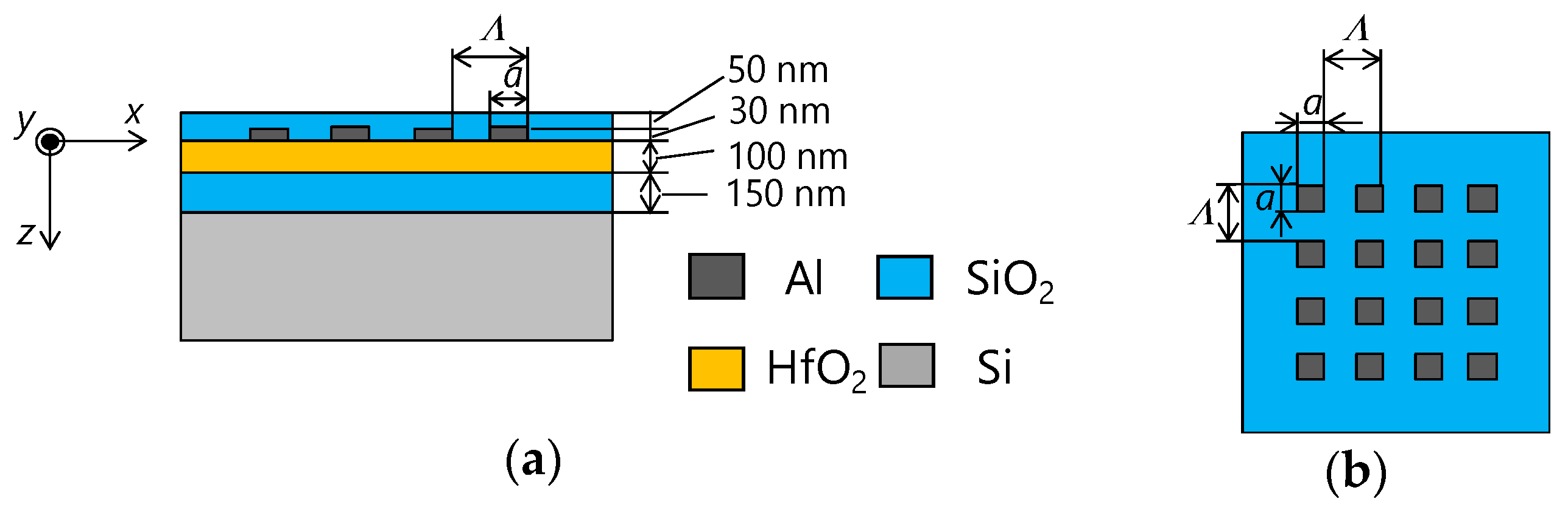
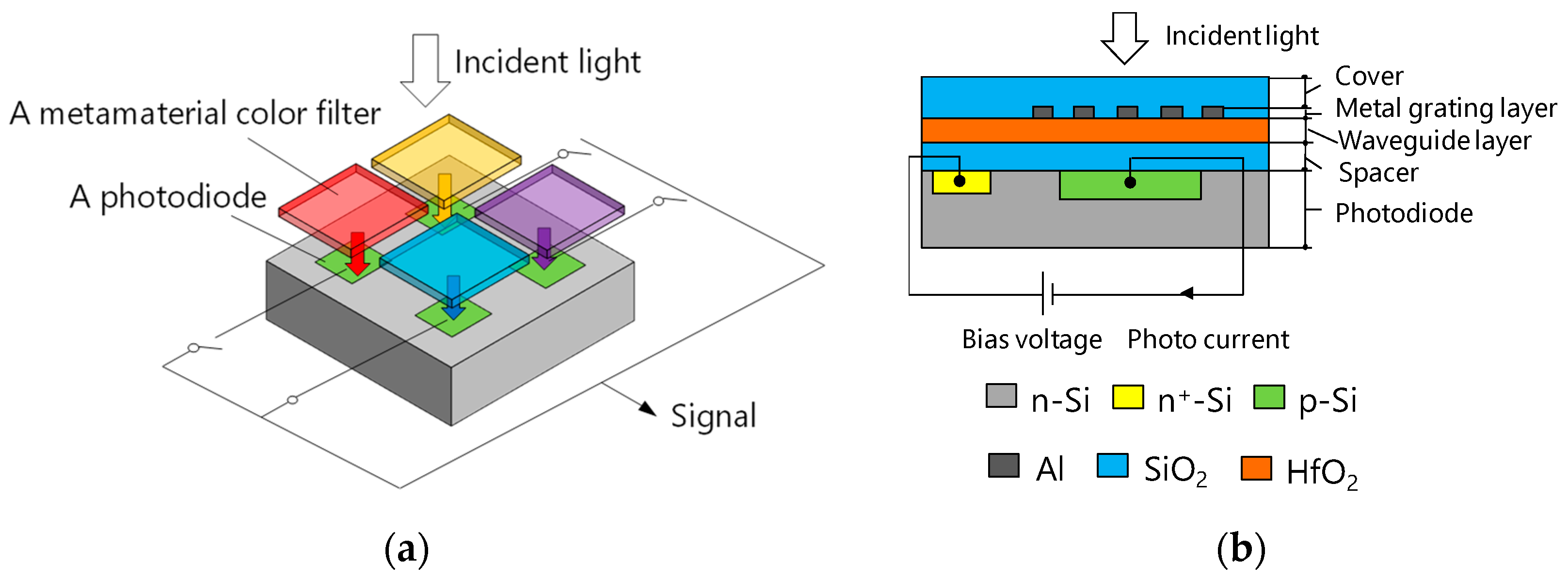
2. Device Configuration

Figure 1a shows a conceptual diagram of the proposed spectroscopic device. A plurality of color sensors with different spectral sensitivity characteristics, in which metamaterial color filters having different spectral characteristics are stacked and arranged on each photodiode, are arranged. Incident wavelengths selected by the color filters enter the photodiodes, the output signals of the photodiodes are sequentially read out, and the spectral characteristics of the incident light are obtained by calculation processing. Figure 1b shows the cross-sectional view of a color sensor consisting of a metamaterial color filter formed on an Si photodiode through a spacer layer. The metamaterial color filter consists of a guided-mode resonant metal grating covered with a SiO2 layer.
The guided-mode resonant metal grating consists of a 2D Al grating layer formed on an HfO2 guided layer. The guided layer is formed on the SiO2 spacer layer. Since the effective refractive index of the guided layer is higher than that of the surroundings, the guided layer functions as a planar waveguide and strongly confines the resonant wavelength. Transmitted light generates only zeroth order diffraction because the grating period is smaller than the resonant wavelength. The grating groove is filled with SiO2. Incident light is impinged from the SiO2 cover layer. Photocurrent generated in the photodiode is read out as an output signal. By changing the period of the metal grating layer of each color filter, it is possible to control the resonant wavelength and to extract spectral information from each photodiode.

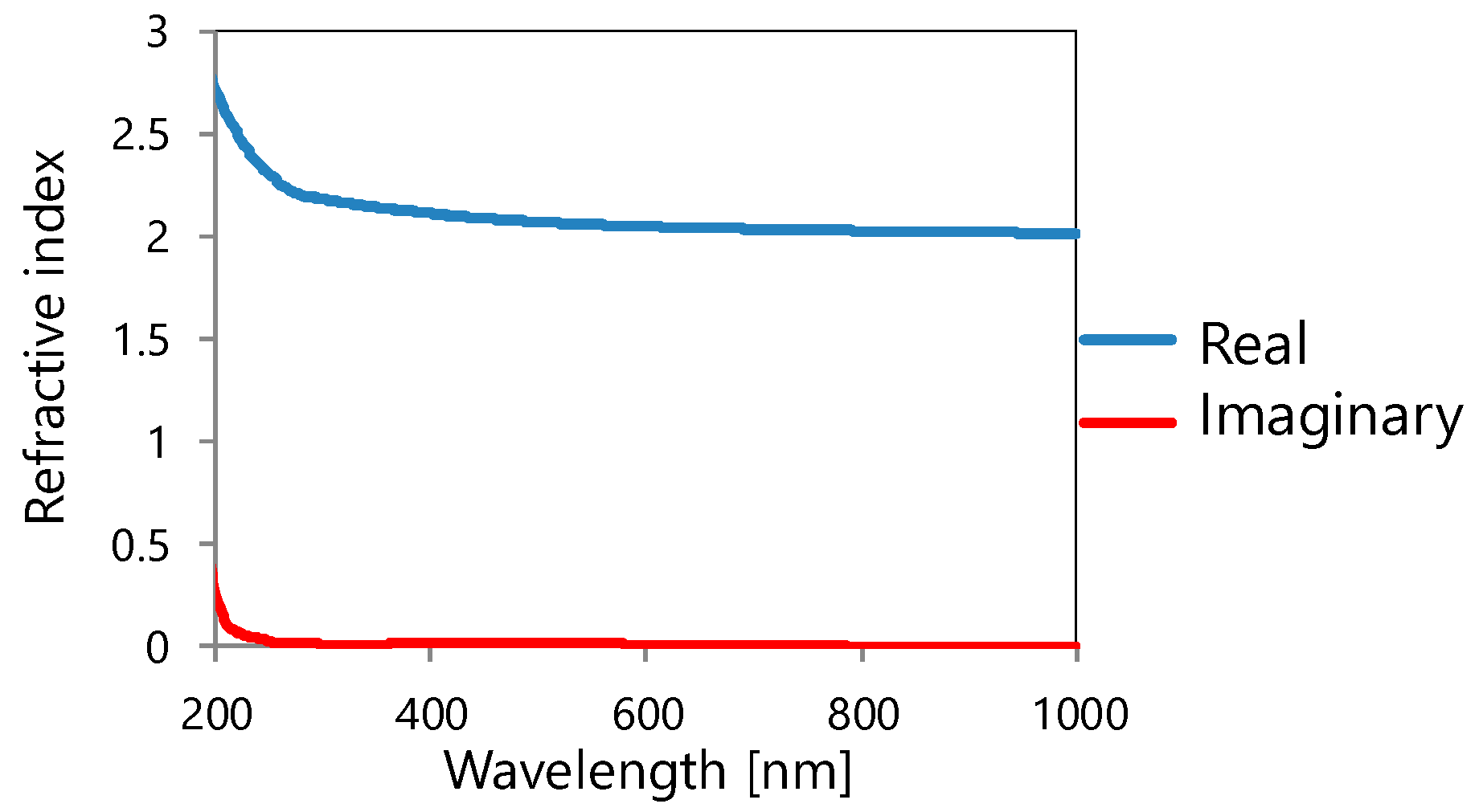
3. Design and Numerical Analysis

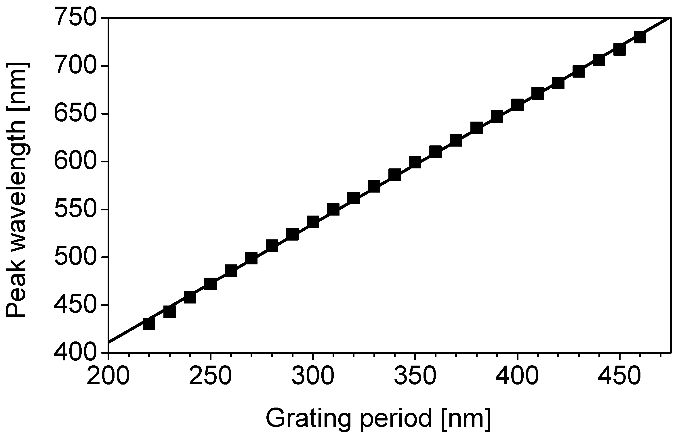
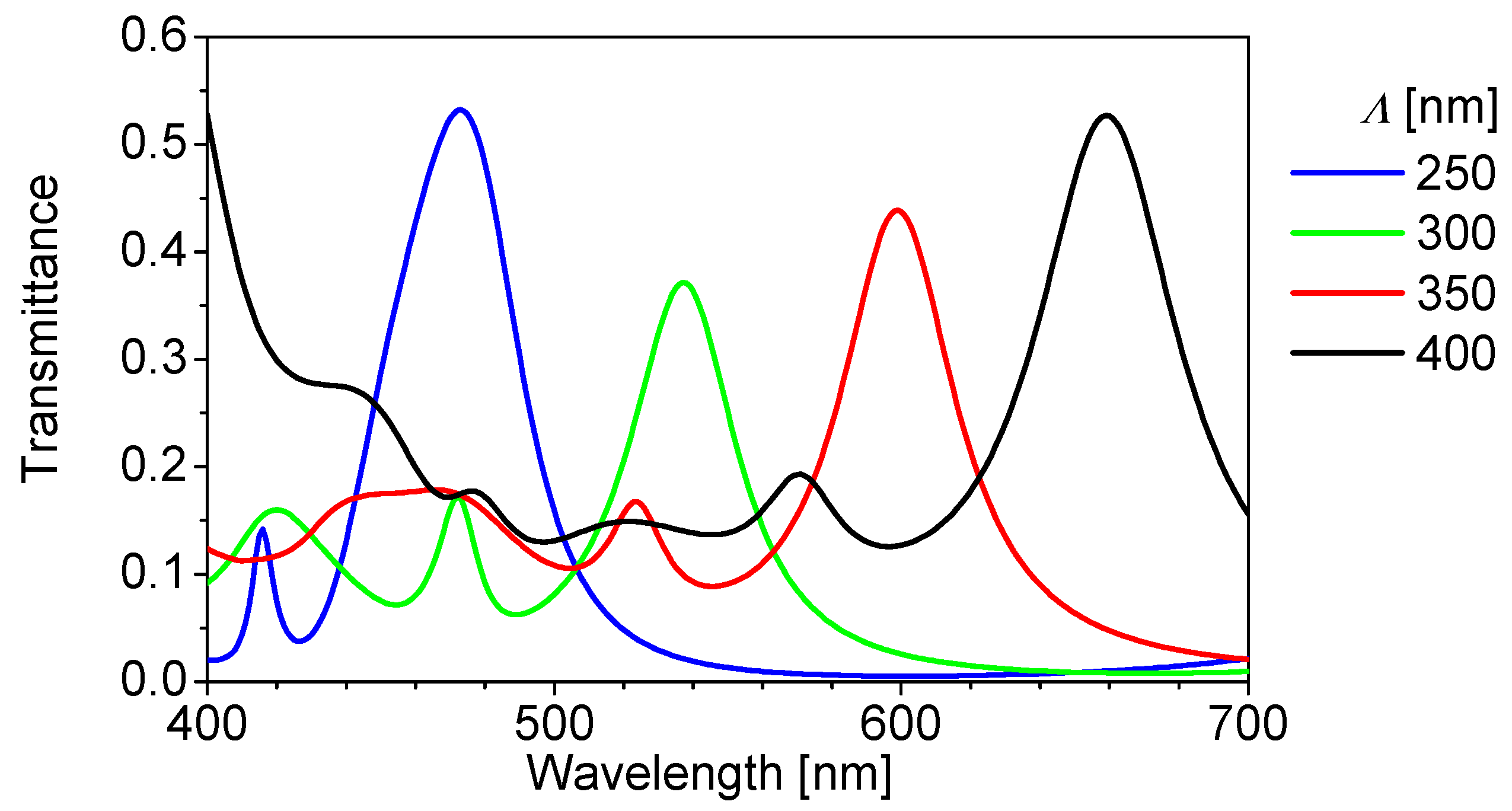
3.1. Design of Color Filters

Numerical analysis was carried out using rigorous coupled-wave analysis (RCWA), which yields accurate results using Maxwell’s equations in the frequency domain [37,38]. Figure 2 shows a calculation model of one color filter element. The electric field, magnetic field, and propagation direction of incident light are parallel to the x, y, and z axes, respectively. A 50-nm-thick SiO2 cover layer, 30-nm-thick 2D-periodic Al nanodot array, 100-nm-thick HfO2 waveguide layer, and a 150-nm-thick SiO2 spacer are formed on an Si substrate of photodiode. Here, Λ and a are the grating period and nanodot size, respectively. The color filters have polarization independent because of 2D subwavelength gratings with the same periods for the x and y directions.
Normally, incident light from outside was made to pass through the cover layer, and transmittance spectrum at the Si side of the SiO2/Si interface was calculated to obtain spectral characteristics of the device. For optical designing of the structure integrated with the color filter and photodiode, spectral characteristics, including the influence of reflection and interference by the Si substrate, were calculated instead of just obtaining the transmission spectrum of only the color filter. The incident light polarized along the x-axis was normally incident and the total transmittance obtained by combining all the transmitted diffracted waves was calculated. Refractive indices of Al, Si, and SiO2 in references [39,40,41], respectively, were used for the calculation. Figure 3 shows real and imaginary parts of the refractive index of HfO2 used for the calculation, which was measured by a spectroscopic ellipsometer.
Figure 4 shows the calculated transmittance spectra penetrating a Si substrate for several grating periods. Here, a/Λ was fixed to be 0.8. Figure 4 illustrates that the peak wavelength of the transmission spectrum can be controlled mainly through the grating period. The peak wavelength is shifted to the longer wavelength side as the period increases, which agrees with the principle of guided-mode resonant gratings. From this result, we could design the structures that exhibit functions of spectroscopes, including a reflection and interference effect, due to the influence of the interface between the SiO2 space and Si photodiode. The output signal actually obtained by the color sensor is outputted as a characteristic signal, which is the product of the transmission spectrum shown in Figure 4 and the spectral sensitivity characteristic of the Si photodiode.
Figure 5 shows the peak wavelength as a function of the grating period extracted from the results of Figure 4. It can be seen that the peak wavelength shifts in proportion to the grating period in the entire visible wavelength range. The linear fitting equation for Figure 5 is given by the following equation:
λ peak = 1.24 × Λ + 163.4
Here, λpeak is a peak wavelength.

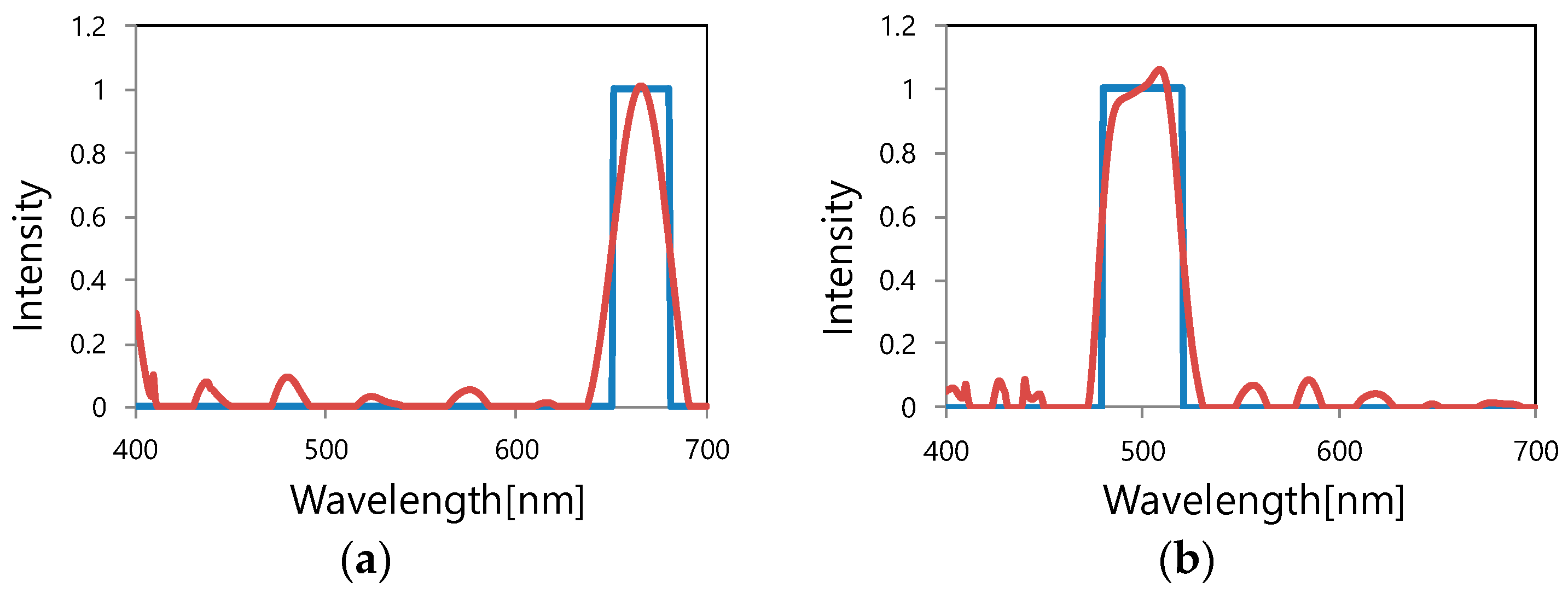
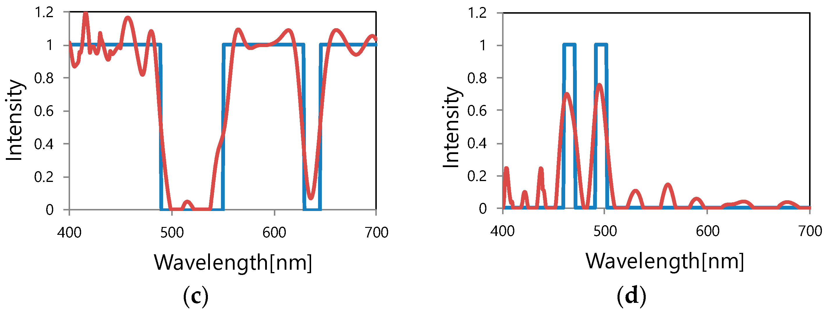
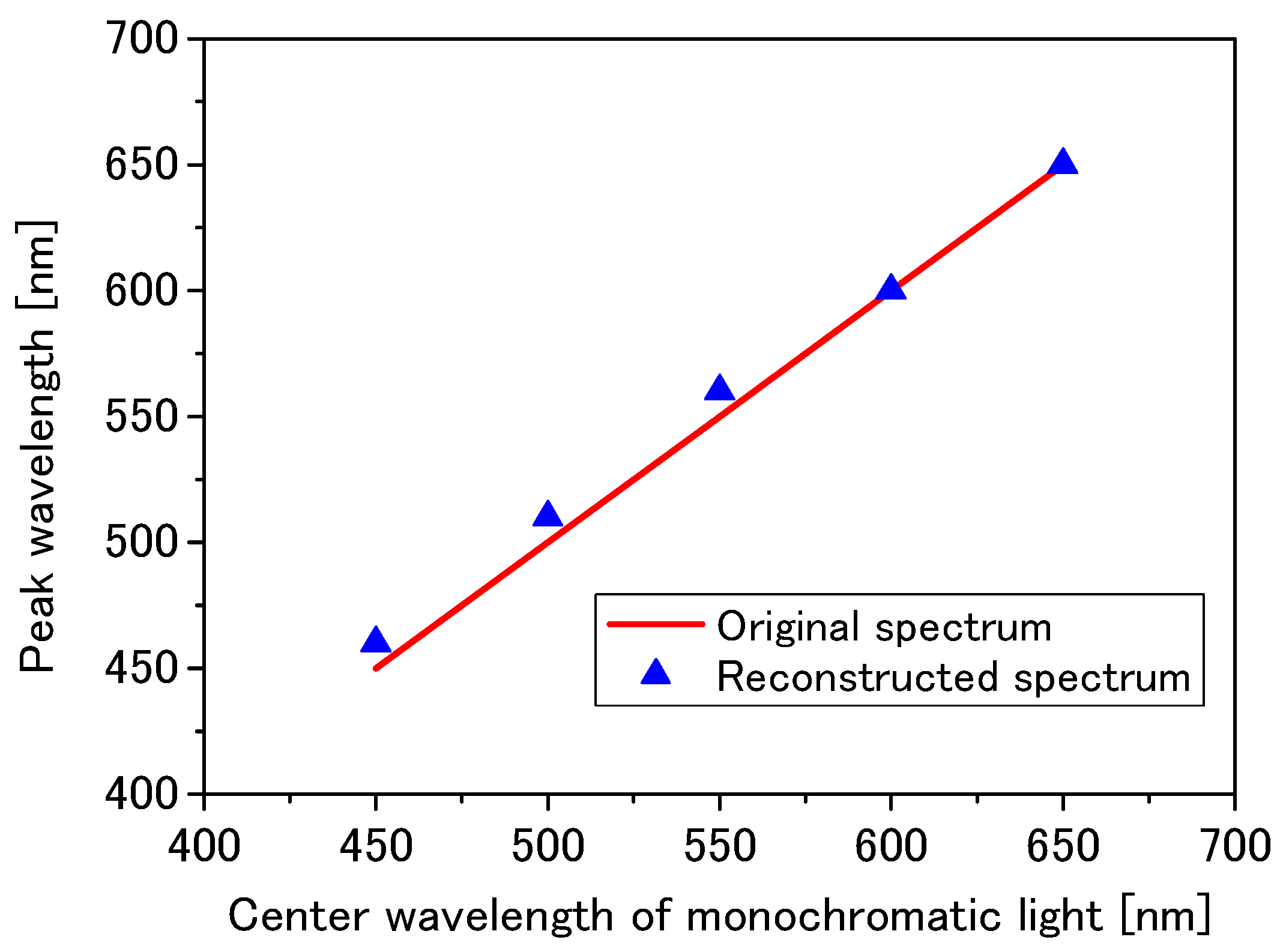
3.2. Spectrum Reconstruction: Principle and Calculation Examples
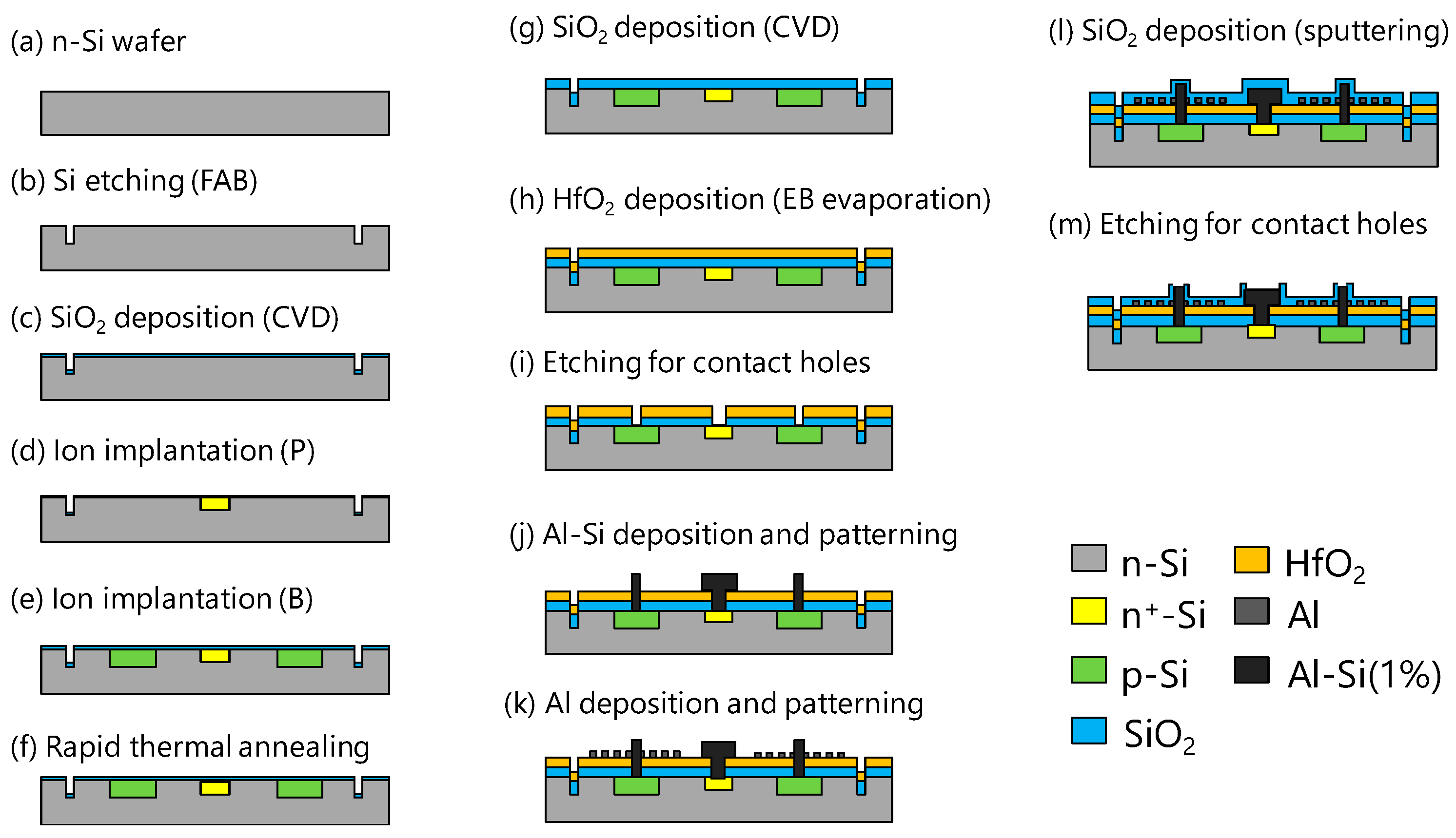
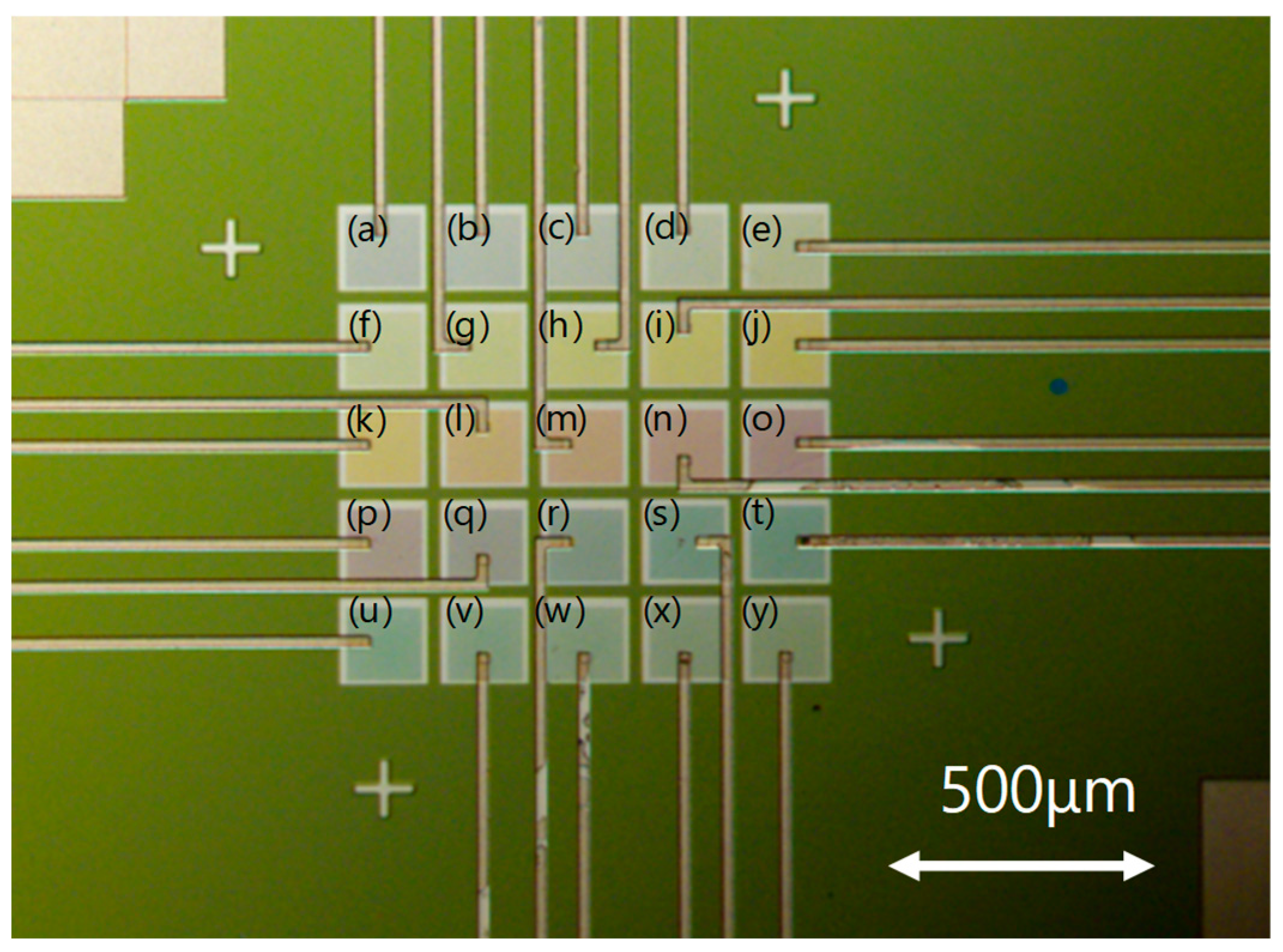
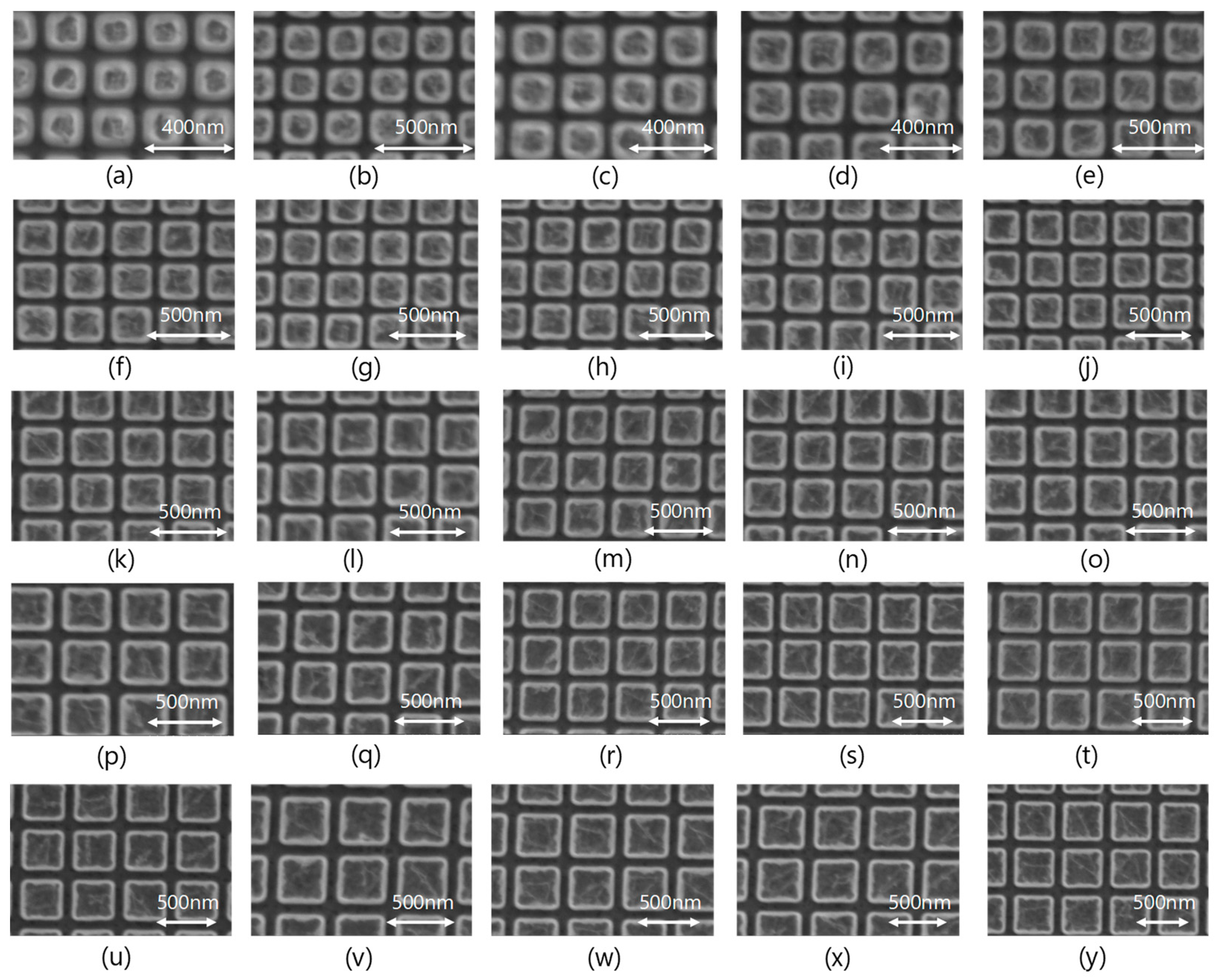
An output signal from each color sensor is the integrated amount of the energy spectrum received by each photodiode and it cannot be decomposed into spectral components. Therefore, in order to reconstruct the spectral characteristic of the input light from the output signal, calculation between output signals is required. To solve the inverse problem of determining the input signals (spectrum of incident light) from the output signals, spectral characteristics are calculated using the Tikhonov regularization method [42]. Consider a spectroscopic device composed of b color sensors. b is the number of color sensors. The photocurrent of each color sensor is obtained as a product of the spectral characteristic of incident light and the wavelength sensitivity characteristic of each color sensor, integrated over the wavelength. The photocurrent is expressed in matrix format as follows:
O = S I
Here, O (A) is a 1 × b column vector of photocurrent. S (A/W) is a b × c matrix of wavelength sensitivity, and I (W) is a 1 × c column vector of spectral characteristics of incident light. c is a wavelength division number. O and S are measured experimentally, and I is to be determined. In order to solve this inverse problem, I is calculated using the matrix, M, obtained by the Tikhonov regularization method, as shown below:
I = M O  
M is a c × b matrix. Besides, because the spectral characteristic cannot be a negative value, the following condition is added:
I = I   ( I > 0 )   or   0   ( I 0 )
Equations (3) and (4) are solved to obtain the spectral characteristics.
Next, several incident light spectra were designed (designed spectra) and compared with the incident light spectra (reconstructed spectra) calculated using Equations (3) and (4). It should be noted that b was set to 25 and the calculated wavelength range to be integrated was 400 to 700 nm. Twenty-five color filters with different grating periods between 210 and 450 nm at intervals of 10 nm were used for the matrix, S. Some of the 25 filter characteristics are shown in Figure 4. Here, the sensitivity of the Si photodiode is ignored for simplicity.
The calculation results are shown in Figure 6. As shown in Figure 6a,b, the peak positions of the designed spectrum and the reconstructed spectrum coincide with each other, and the bandwidths also substantially coincide. However, the sharp edges of the designed spectrum take rounded shapes like the Gaussian distribution in the reconstructed spectrum. This can be attributed to the coarse resolution because just 25 filters are provided across a wavelength range of 300 nm. It can be improved by increasing the number of filters. Moreover, as can be seen from Figure 6c,d, it is possible to calculate the results for multiple peaks. Figure 6d reveals that as the width of the designed spectrum becomes narrower, the peak position of reconstructed data is in good agreement with the designed peak position, but the peak intensity of the reconstructed spectrum decreases. These results suggest that optical spectra in a wavelength range of 400 to 700 nm can be obtained by using the proposed devices; however, there is room for improvement.

4. Fabrication

Figure 7 shows the process steps. An n-type Si substrate of a 400 μm thickness is etched by a fast atom beam (FAB) to form alignment marks (Figure 7a,b). Next, to prevent metal contamination, an SiO2 protective film with a thickness of 5 nm is formed by chemical vapor deposition (CVD) (Figure 7c). Then, P ions are implanted into the contact area of electrodes to form n+ -Si (Figure 7d). After that, ion implantation of B is performed to form p-Si (Figure 7e). Besides, rapid thermal annealing is performed to activate ions simultaneously with the recovery of crystal from damage due to ion implanted ions (Figure 7f). Next, as a spacer, SiO2 is formed by CVD (Figure 7g). Then, as a waveguide layer, HfO2 is deposited by electron-beam (EB) evaporation (Figure 7h).
After that, SiO2 and HfO2 etching is performed to make contact holes (Figure 7i). Next, the Al-Si (1%) layer with a thickness of 400 nm is formed by sputtering, and wet etching is performed to form electrodes (Figure 7j). After Al film formation by sputtering, nanodot array structures are patterned by EB lithography, followed by FAB etching (Figure 7k). Next, an SiO2 cover layer is formed by sputtering (Figure 7l). Finally, SiO2 in the electrode pad portion is etched (Figure 7m).
Figure 8 shows a reflection image of an optical microscope of color filters fabricated on a photodiode array. The filters are fabricated in 25 patterns, with grating periods between 220 and 460 nm at increments of 10 nm, which correspond (a) to (y) in the figure. All filters are 150 μm × 150 μm in size. Although the color filter is designed as a transmissive type, the structural color, which depends on the period of the structure, can also be confirmed in the reflected images. The wiring pattern connected from each photodiode can also be confirmed.
Figure 9 shows scanning electron microscope (SEM) images of the fabricated color filters corresponding to the symbols (a) to (y) of Figure 8. All filters are designed to be 0.8 of the a/Λ ratio. It can be seen that all the filters are fabricated accurately.

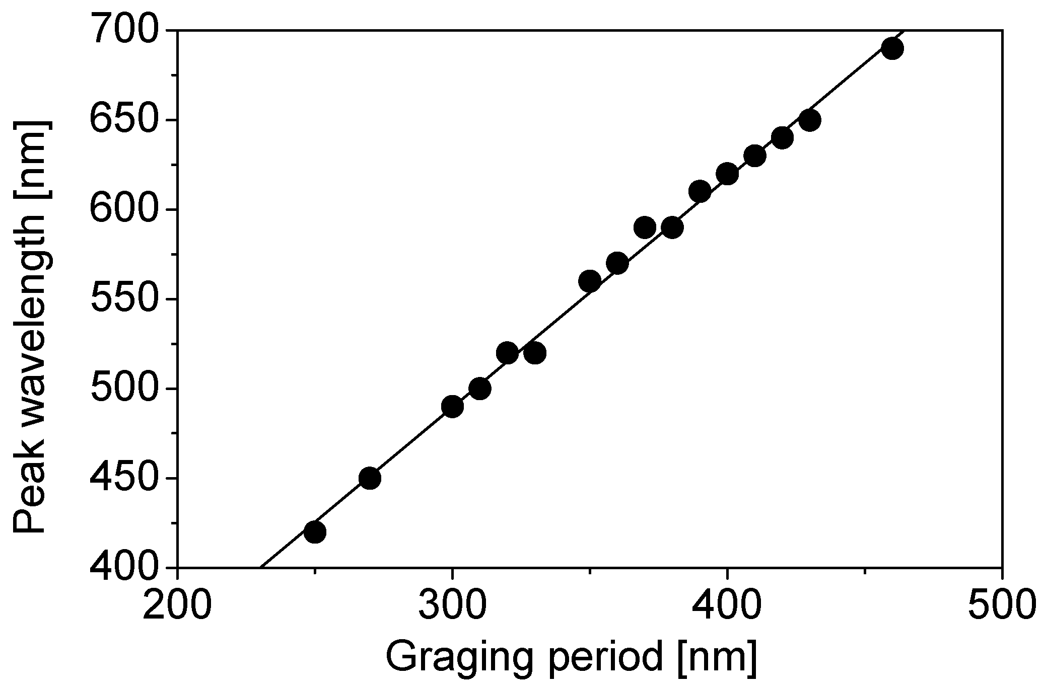
5. Measured Results and Discussion

Spectral sensitivity characteristics of color sensors were measured using a broadband spectral response measurement system (CEP-25BXS, Bunkou Keiki Co., Ltd., Tokyo, Japan). In this measurement, the wavelength resolution was set to 10 nm. Different color sensors exhibited different spectral sensitivity characteristics. Figure 10 shows the relationship between the grating period and the peak wavelength of the spectral sensitivity. The peak wavelength is linearly dependent on the grating period, and the slope of the straight line almost agrees with that of the calculated peak wavelength shift of the color filters shown in Figure 5. The linear fitting equation for Figure 10 is given by the following equation:
λ peak = 1.28 × Λ + 105.4
When the monochromatic light with wavelengths of 450, 500, 550, 600, and 650 nm is incident, the spectral characteristics of the incident light are reconstructed from the output signals obtained by the respective color sensors. Spectral characteristics of the reconstructed incident light are shown with solid lines in Figure 11. For comparison, spectral characteristics of the incident light measured with a commercially available spectrometer (HR4000CG-UV-NIR, Ocean optics, Inc., Largo, FL, USA) are shown as original spectra with dotted lines. The peak wavelength of the reconstructed spectrum can be confirmed to be near that of the original spectrum. Therefore, we believe that the spectroscopic measurement was successfully performed using the fabricated device. However, reconstructed spectra become broader compared to the original spectra. This increment in width can be attributed to the coarse resolution because only 25 filters are provided across a wavelength range of 300 nm. The reconstructed spectra can be improved by increasing the number of filters.
Figure 12 shows the relationship between the peak wavelengths of reconstructed spectra and the center wavelength of monochromatic lights extracted from the results of Figure 11. It is found that the peak wavelengths of the reconstructed spectra are in good agreement with the center wavelengths of the monochromatic lights.

6. Conclusions

We fabricated a filter array spectroscope consisting of metamaterial color filters and Si photodiodes. The color filters based on guided-mode resonant metal gratings were newly designed. The peak wavelength of the transmission spectrum could be controlled mainly by the grating period. The filters were fabricated in 25 patterns, with grating periods between 220 and 460 nm at increments of 10 nm. SEM images of fabricated color filters confirmed that all the filters were fabricated accurately. The peak wavelength of the spectral sensitivity was found to be linearly dependent on the grating period. Several monochromatic lights were made incident on the fabricated device and the spectral characteristics of the incident light were reconstructed from the output signals obtained from the respective color sensors. The peak wavelengths of the reconstructed spectra were in good agreement with the center wavelengths of the monochromatic lights.

Author Contributions

Conceptualization, Y.K.; methodology, Y.K.; software, D.E.; validation, Y.K., D.E. and K.H.; formal analysis, Y.K. and D.E.; investigation, Y.K., D.E. and K.H.; resources, Y.K., D.E. and K.H.; data curation, D.E. and Y.K.; writing—original draft preparation, Y.K.; writing—review and editing, Y.K.; visualization, D.E. and Y.K.; supervision, K.H.; project administration, Y.K.; funding acquisition, Y.K.

Funding

A part of this research was funded by the MEXT KAKENHI 16K13648 and 16H04342.

Acknowledgments

Authors thank H. Sai for providing technical support for spectral response measurement. A part of this research was performed in Micro/Nano-Machining Research and Education Center (Tohoku University) and the Center for Integrated Nano Technology Support (Tohoku University) with assistance of MEXT Nanotechnology Platform.

Conflicts of Interest

The authors declare no conflict of interest.

References

  1. Ebbesen, T.W.; Lezec, H.J.; Ghaemi, H.F.; Thio, T.; Wolff, P.A. Extraordinary optical transmission through sub-wavelength hole arrays. Nature 1998, 391, 667–669. [Google Scholar] [CrossRef]
  2. Genet, C.; Ebbesen, T.W. Light in tiny holes. Nature 2007, 445, 39–46. [Google Scholar] [CrossRef] [PubMed]
  3. Kaplan, A.F.; Xu, T.; Guo, L.J. High efficiency resonance-based spectrum filters with tunable transmission bandwidth fabricated using nanoimprint lithography. Appl. Phys. Lett. 2011, 99, 143111. [Google Scholar] [CrossRef]
  4. Xu, T.; Wu, Y.K.; Luo, X.; Guo, L.J. Plasmonic nanoresonators for high-resolution colour filtering and spectral imaging. Nat. Commun. 2010, 1, 59. [Google Scholar] [CrossRef] [PubMed]
  5. Lee, H.S.; Yoon, Y.T.; Lee, S.S.; Kim, S.H.; Lee, K.D. Color filter based on a subwavelength patterned metal grating. Opt. Express 2007, 15, 15457–15463. [Google Scholar] [CrossRef] [PubMed]
  6. Chen, Q.; Cumming, D.R.S. High transmission and low color cross-talk plasmonic color filters using triangular-lattice hole arrays in aluminum films. Opt. Express 2010, 18, 14056–14062. [Google Scholar] [CrossRef] [PubMed]
  7. Chou, S.Y.; Krauss, P.R.; Renstrom, P.J. Nanoimprint lithography. J. Vac. Sci. Technol. B 1996, 14, 4129–4133. [Google Scholar] [CrossRef]
  8. Chou, S.Y.; Krauss, P.R.; Zhang, W.; Guo, L.; Zhuang, L. Sub-10 nm imprint lithography and applications. J. Vac. Sci. Technol. B 1997, 15, 2897–2904. [Google Scholar] [CrossRef]
  9. Bao, L.R.; Cheng, X.; Huang, X.D.; Guo, L.J.; Pang, S.W.; Yee, A.F. Nanoimprinting over topography and multilayer three-dimensional printing. J. Vac. Sci. Technol. B 2002, 20, 2881–2886. [Google Scholar] [CrossRef]
  10. Zhang, W.; Chou, S.Y. Fabrication of 60-nm transistors on 4-in. wafer using nanoimprint at all lithography levels. Appl. Phys. Lett. 2003, 83, 1632–1634. [Google Scholar] [CrossRef]
  11. Alkaisi, M.M.; Jayatissa, W.; Konijn, M. Multilevel nanoimprint lithography. Curr. Appl. Phys. 2004, 4, 111–114. [Google Scholar] [CrossRef]
  12. Roy, E.; Kanamori, Y.; Belotti, M.; Chen, Y. Enhanced UV imprint ability with a tri-layer stamp configuration. Microelectron. Eng. 2005, 78–79, 689–694. [Google Scholar] [CrossRef]
  13. Kanamori, Y.; Okochi, M.; Hane, K. Fabrication of antireflection subwavelength gratings at the tips of optical fibers using UV nanoimprint lithography. Opt. Express 2013, 21, 322–328. [Google Scholar] [CrossRef] [PubMed]
  14. Ito, S.; Kikuchi, E.; Watanabe, M.; Sugiyama, Y.; Kanamori, Y.; Nakagawa, M. Silica imprint templates with concave patterns from single-digit nanometers fabricated by electron beam lithography involving argon ion beam milling. Jpn. J. Appl. Phys. 2017, 56, 06GL01. [Google Scholar] [CrossRef]
  15. Lee, S.W.; Lee, K.S.; Ahn, J.; Lee, J.J.; Kim, M.G.; Shin, Y.B. Highly sensitive biosensing using arrays of plasmonic Au nanodisks realized by nanoimprint lithography. ACS Nano 2011, 5, 897–904. [Google Scholar] [CrossRef] [PubMed]
  16. Peer, A.; Biswas, R. Extraordinary optical transmission in nanopatterned ultrathin metal films without holes. Nanoscale 2016, 8, 4657–4666. [Google Scholar] [CrossRef] [PubMed]
  17. Nishiguchi, K.; Sueyoshi, K.; Hisamoto, H.; Endo, T. Fabrication of gold-deposited plasmonic crystal based on nanoimprint lithography for label-free biosensing application. Jpn. J. Appl. Phys. 2016, 55, 08RE02. [Google Scholar] [CrossRef]
  18. Peer, A.; Hu, Z.; Singh, A.; Hollingsworth, J.A.; Biswas, R.; Htoon, H. Photoluminescence enhancement of CuInS2 quantum dots in solution coupled to plasmonic gold nanocup array. Small 2017, 13, 1700660. [Google Scholar] [CrossRef] [PubMed]
  19. Hutley, M.C. Diffraction gratings. In Diffractive Optics for Industrial and Commercial Applications; Turunen, J., Wyrowski, F., Eds.; Akademie Verlag: Berlin, Germany, 1997; pp. 59–80. ISBN 3055017331. [Google Scholar]
  20. Ema, D.; Kanamori, Y.; Sai, H.; Hane, K. Plasmonic color filters integrated on a photodiode array. Electron. Commun. Jpn. 2018, 101, 95–104. [Google Scholar] [CrossRef]
  21. Chang, C.C.; Lin, N.T.; Kurokawa, U.; Choi, B.I. Spectrum reconstruction for filter-array spectrum sensor from sparse template selection. Opt. Eng. 2011, 50, 114402. [Google Scholar] [CrossRef]
  22. Kurokawa, U.; Choi, B.I.; Chang, C.C. Filter-Based Miniature Spectrometers: Spectrum Reconstruction Using Adaptive Regularization. IEEE Sens. J. 2011, 11, 1556–1563. [Google Scholar] [CrossRef]
  23. Chang, C.C.; Lin, H.Y. Spectrum Reconstruction for On-Chip Spectrum Sensor Array Using a Novel Blind Nonuniformity Correction Method. IEEE Sens. J. 2012, 12, 2586–2592. [Google Scholar] [CrossRef]
  24. Chang, C.C.; Su, Y.J.; Kurokawa, U.; Choi, B.I. Interference Rejection Using Filter-Based Sensor Array in VLC Systems. IEEE Sens. J. 2012, 12, 1025–1032. [Google Scholar] [CrossRef]
  25. Oliver, J.; Lee, W.B.; Lee, H.N. Filters with random transmittance for improving resolution in filter-array-based spectrometers. Opt. Express 2013, 21, 3969–3989. [Google Scholar] [CrossRef] [PubMed]
  26. Oliver, J.; Lee, W.; Park, S.; Lee, H.N. Improving resolution of miniature spectrometers by exploiting sparse nature of signals. Opt. Express 2012, 20, 2613–2625. [Google Scholar] [CrossRef] [PubMed]
  27. Norton, S.M.; Erdogan, T.; Morris, G.M. Coupled-mode theory of resonant-grating filters. J. Opt. Soc. Am. A 1997, 14, 629–639. [Google Scholar] [CrossRef]
  28. Jacob, D.K.; Dunn, S.C.; Moharam, M.G. Design considerations for narrow-band dielectric resonant grating reflection filters of finite length. J. Opt. Soc. Am. A 2000, 17, 1241–1249. [Google Scholar] [CrossRef]
  29. Brundrett, D.L.; Glytsis, E.N.; Gaylord, T.K.; Bendickson, J.M. Effects of modulation strength in guided-mode resonant subwavelength gratings at normal incidence. J. Opt. Soc. Am. A 2000, 17, 1221–1230. [Google Scholar] [CrossRef]
  30. Peters, D.W.; Kemme, S.A.; Hadley, G.R. Effect of finite grating, waveguide width, and end-facet geometry on resonant subwavelength grating reflectivity. J. Opt. Soc. Am. A 2004, 21, 981–987. [Google Scholar] [CrossRef]
  31. Kobayashi, T.; Kanamori, Y.; Hane, K. Surface laser emission from solid polymer dye in a guided mode resonant grating filter structure. Appl. Phys. Lett. 2005, 87, 151106. [Google Scholar] [CrossRef]
  32. Kanamori, Y.; Kitani, T.; Hane, K. Guided-Mode Resonant Grating Filter Fabricated on Silicon-on-Insulator Substrate. Jpn. J. Appl. Phys. 2006, 45, 1883–1885. [Google Scholar] [CrossRef]
  33. Kanamori, Y.; Kitani, T.; Hane, K. Control of guided resonance in a photonic crystal slab using microelectromechanical actuators. Appl. Phys. Lett. 2007, 90, 031911. [Google Scholar] [CrossRef]
  34. Kanamori, Y.; Katsube, H.; Furuta, T.; Hasegawa, S.; Hane, K. Design and Fabrication of Structural Color Filters with Polymer-Based Guided-Mode Resonant Gratings by Nanoimprint Lithography. Jpn. J. Appl. Phys. 2009, 48, 06FH04. [Google Scholar] [CrossRef]
  35. Kanamori, Y.; Ozaki, T.; Hane, K. Fabrication of Ultrathin Color Filters for Three Primary Colors Using Guided-Mode Resonance in Silicon Subwavelength Gratings. Opt. Rev. 2014, 21, 723–727. [Google Scholar] [CrossRef]
  36. Kanamori, Y.; Ozaki, T.; Hane, K. Reflection color filters of the three primary colors with wide viewing angles using common-thickness silicon subwavelength gratings. Opt. Express 2014, 22, 25663–25672. [Google Scholar] [CrossRef] [PubMed]
  37. Moharam, M.G.; Grann, E.B.; Pommet, D.A.; Gaylord, T.K. Formulation for stable and efficient implementation of the rigorous coupled-wave analysis of binary gratings. J. Opt. Soc. Am. A 1995, 12, 1068–1076. [Google Scholar] [CrossRef]
  38. Lalanne, P.; Morris, G.M. Highly improved convergence of the coupled-wave method for TM polarization. J. Opt. Soc. Am. A 1996, 13, 779–784. [Google Scholar] [CrossRef]
  39. Smith, D.Y.; Shiles, E.; Inokuti, M. The Optical Properties of Metallic Aluminum. In Handbook of Optical Constants of Solids; Palik, E.D., Ed.; Academic Press: Orlando, FL, USA, 1985; Volume 1, pp. 369–406. ISBN 0125444206. [Google Scholar]
  40. Edwards, D.F. Silicon (Si). In Handbook of Optical Constants of Solids; Palik, E.D., Ed.; Academic Press: Orlando, FL, USA, 1985; Volume 1, pp. 547–569. ISBN 0125444206. [Google Scholar]
  41. Philipp, H.R. Silicon Dioxide (SiO2) (Glass). In Handbook of Optical Constants of Solids; Palik, E.D., Ed.; Academic Press: Orlando, FL, USA, 1985; Volume 1, pp. 749–763. ISBN 0125444206. [Google Scholar]
  42. Aster, R.C.; Borchers, B.; Thurber, C.H. Parameter Estimation and Inverse Problems, 2nd ed.; Academic Press: Waltham, MA, USA, 2012; pp. 93–127. ISBN 9780128100929. [Google Scholar]
Figure 1. Schematics of proposed devices. (a) Perspective view in the case of 2 × 2 color sensors; (b) cross-sectional view of one particular color sensor.
Materials 11 01924 g001
Figure 2. Calculation model of one color filter element. (a) Cross-sectional view; (b) top view.
Materials 11 01924 g002
Figure 3. Refractive index of HfO2 used for calculation.
Materials 11 01924 g003
Figure 4. Calculated transmittance spectra penetrating a Si substrate for several grating periods. a/Λ is fixed to be 0.8.
Materials 11 01924 g004
Figure 5. Peak wavelength as a function of grating period, extracted from the results of Figure 4.
Materials 11 01924 g005
Figure 6. Simulation of spectral reconstruction (Blue line: Designed spectrum; red line: Reconstructed spectrum). (a) Single band spectrum near 700 nm in wavelength; (b) single band spectrum at a center wavelength of 500 nm; (c) multiple band-stop spectrum; (d) multiple peak spectrum.
Materials 11 01924 g006aMaterials 11 01924 g006b
Figure 7. Process steps.
Materials 11 01924 g007
Figure 8. Optical microphotographs of fabricated color filters on the photodiode array. (a) Λ = 220 nm, (b) Λ = 230 nm, (c) Λ = 240 nm, (d) Λ = 250 nm, (e) Λ = 260 nm, (f) Λ = 270 nm, (g) Λ = 280 nm, (h) Λ = 290 nm, (i) Λ = 300 nm, (j) Λ = 310 nm, (k) Λ = 320 nm, (l) Λ = 330 nm, (m) Λ = 340 nm, (n) Λ = 350 nm, (o) Λ = 360 nm, (p) Λ = 370 nm, (q) Λ = 380 nm, (r) Λ = 390 nm, (s) Λ = 400 nm, (t) Λ = 410 nm, (u) Λ = 420 nm, (v) Λ = 430 nm, (w) Λ = 440 nm, (x) Λ = 450 nm, and (y) Λ = 460 nm.
Materials 11 01924 g008
Figure 9. SEM images of fabricated color filters. (a) Λ = 220 nm, (b) Λ = 230 nm, (c) Λ = 240 nm, (d) Λ = 250 nm, (e) Λ = 260 nm, (f) Λ = 270 nm, (g) Λ = 280 nm, (h) Λ = 290 nm, (i) Λ = 300 nm, (j) Λ = 310 nm, (k) Λ = 320 nm, (l) Λ = 330 nm, (m) Λ = 340 nm, (n) Λ = 350 nm, (o) Λ = 360 nm, (p) Λ = 370 nm, (q) Λ = 380 nm, (r) Λ = 390 nm, (s) Λ = 400 nm, (t) Λ = 410 nm, (u) Λ = 420 nm, (v) Λ = 430 nm, (w) Λ = 440 nm, (x) Λ = 450 nm, and (y) Λ = 460 nm.
Materials 11 01924 g009
Figure 10. Dependence of the peak wavelength of the spectral sensitivity on the grating period.
Materials 11 01924 g010
Figure 11. Spectral reconstruction.
Materials 11 01924 g011
Figure 12. Dependence of the peak wavelengths of reconstructed spectra on the center wavelength of the incident monochromatic lights.
Materials 11 01924 g012

