Molybdenum Dichalcogenides for Environmental Chemical Sensing

Abstract
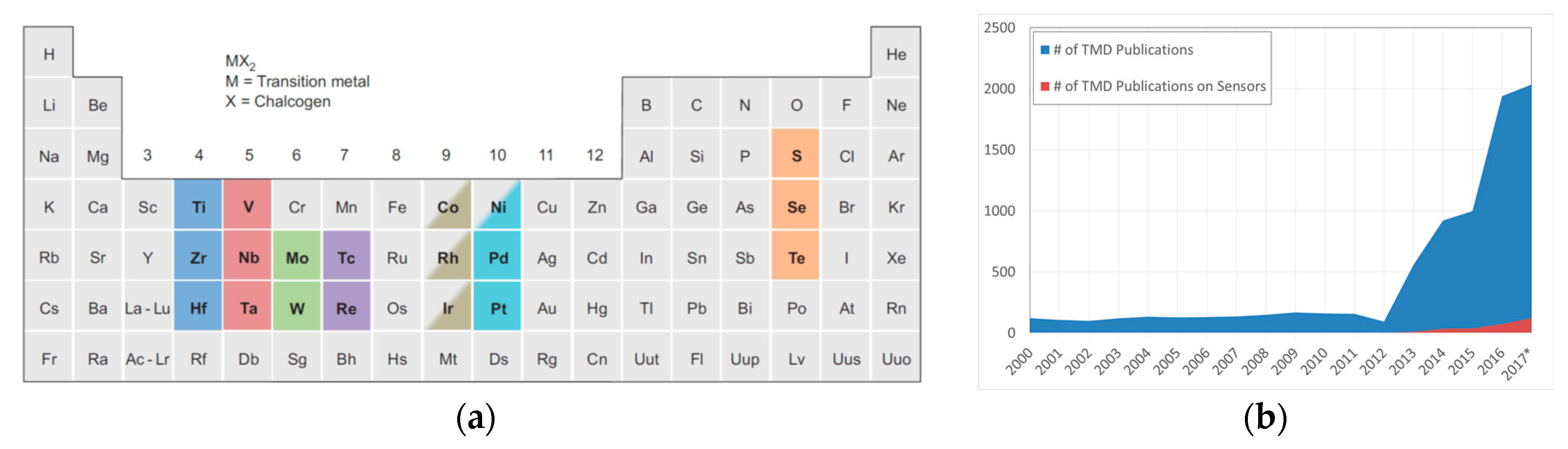
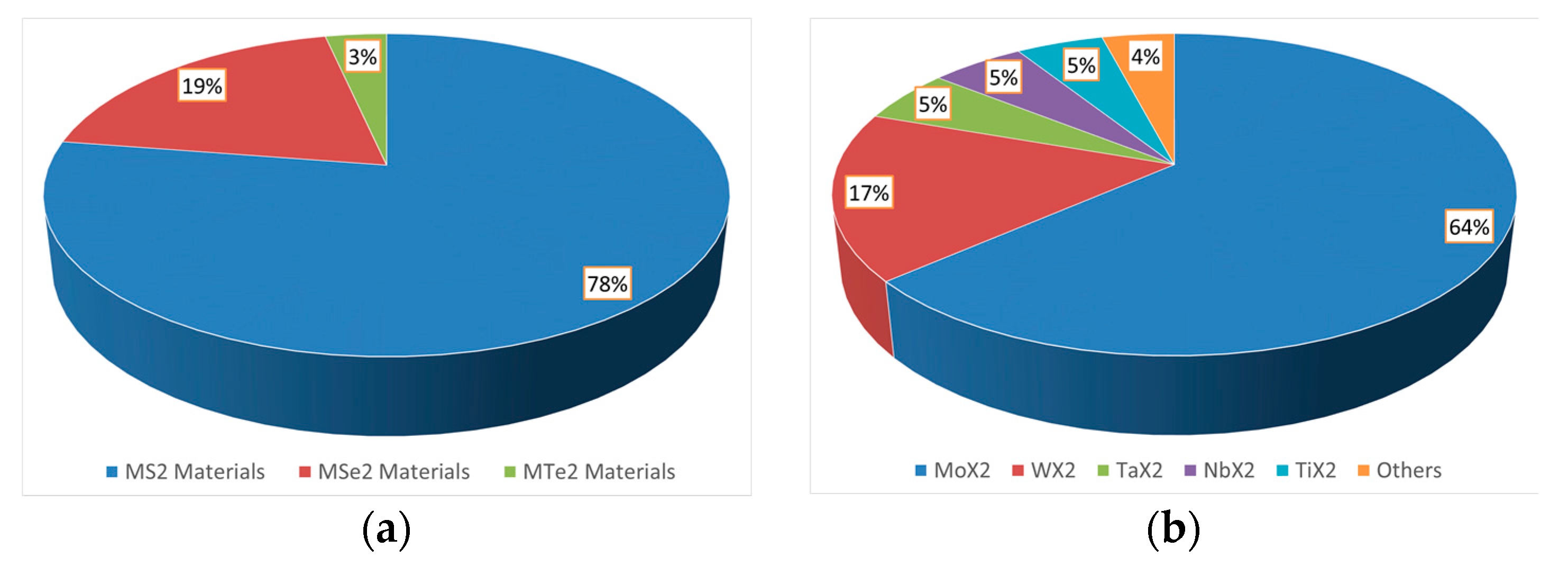
:1. Introduction
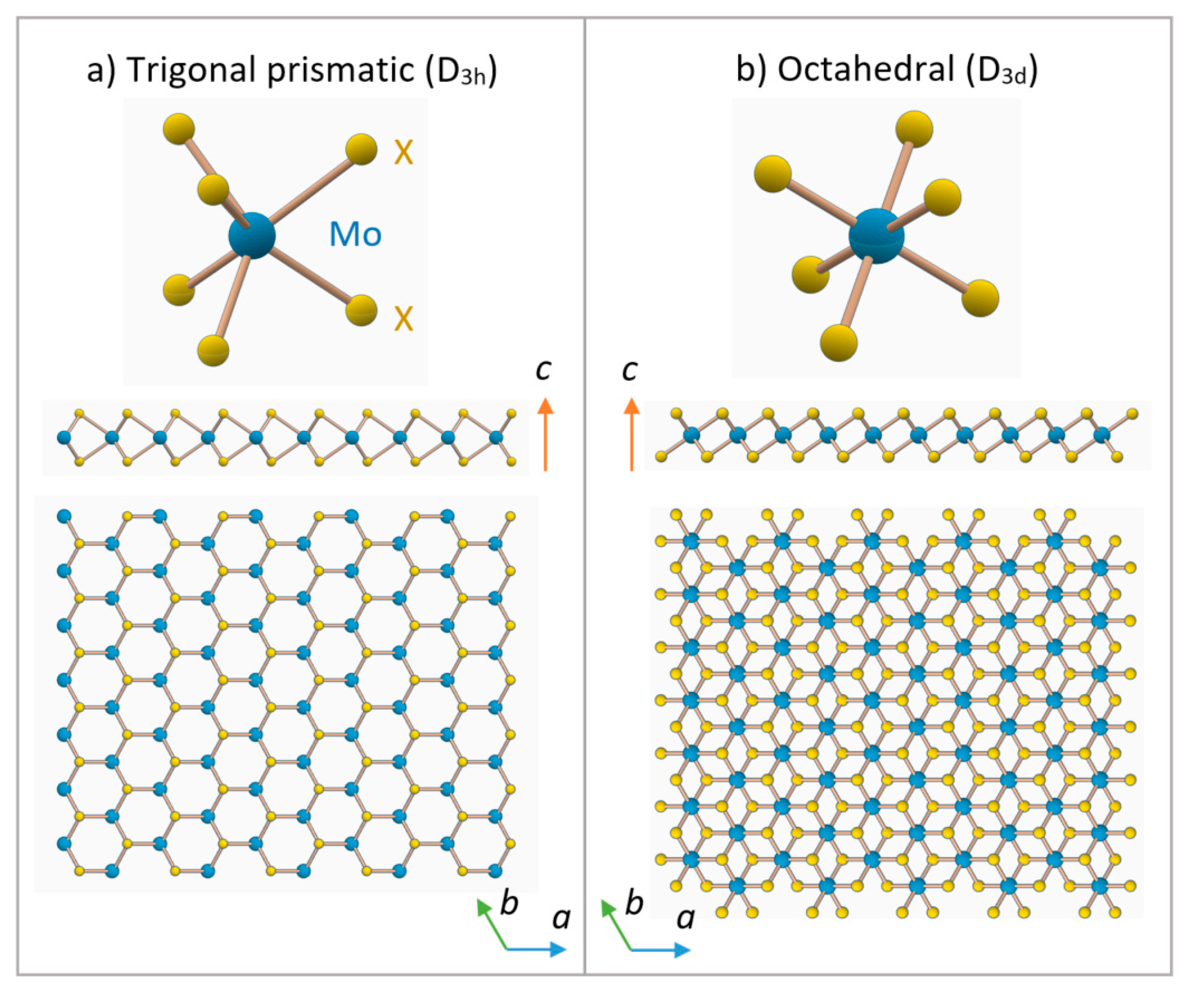
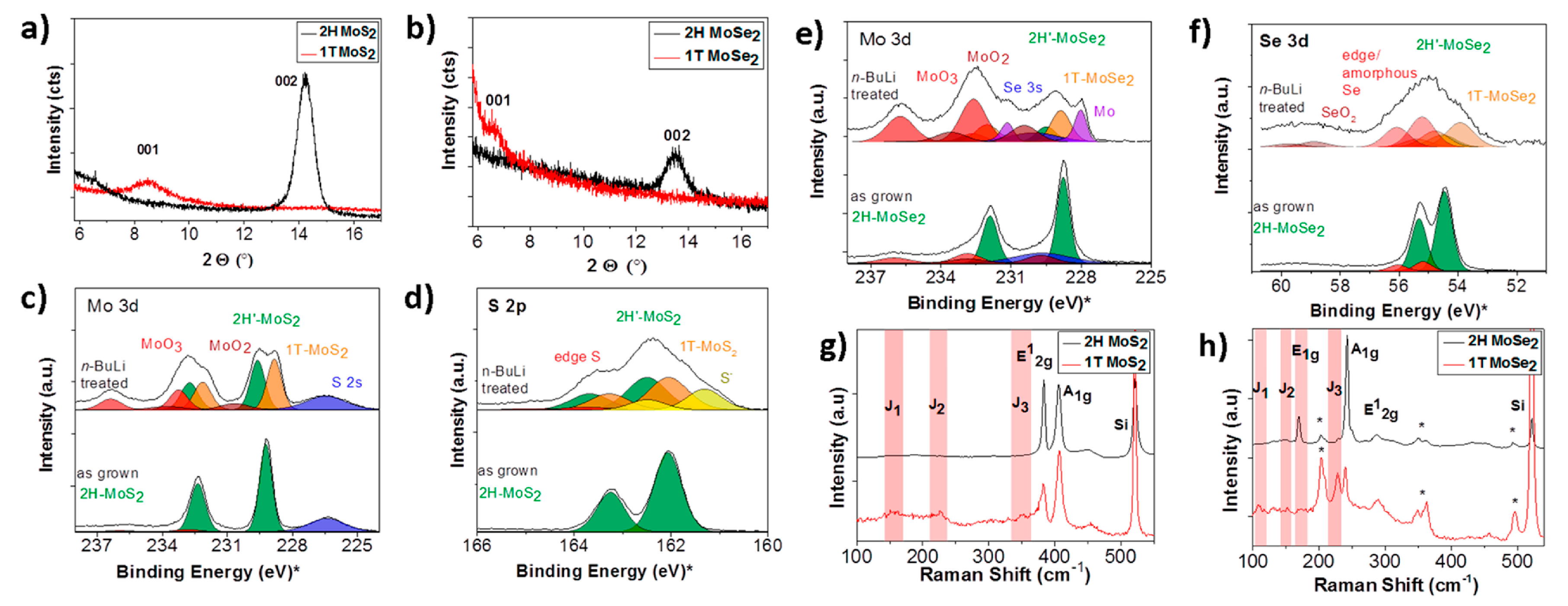
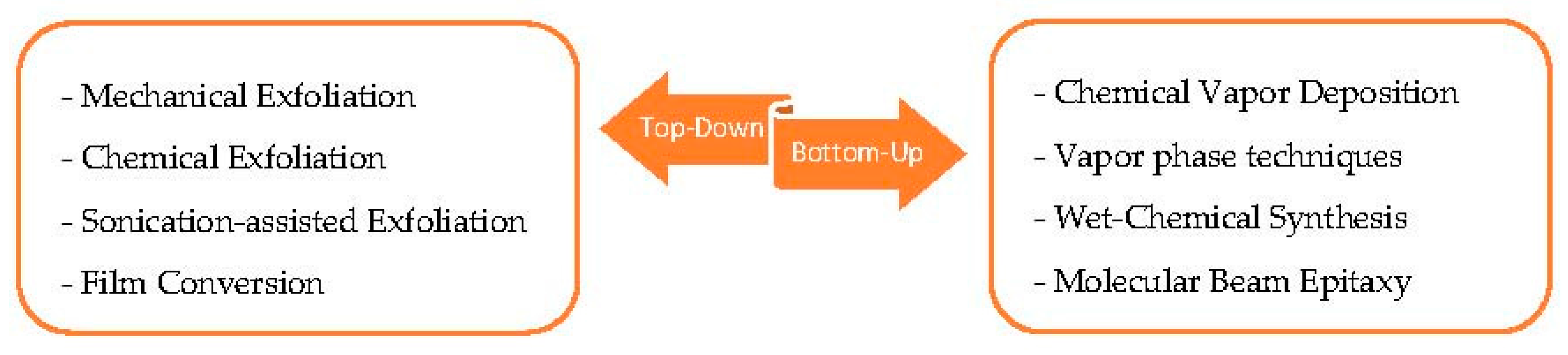
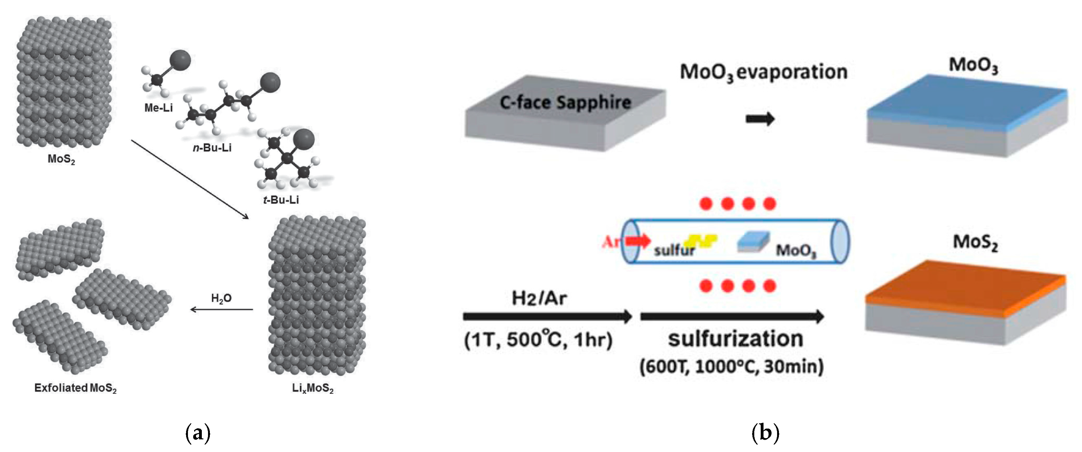
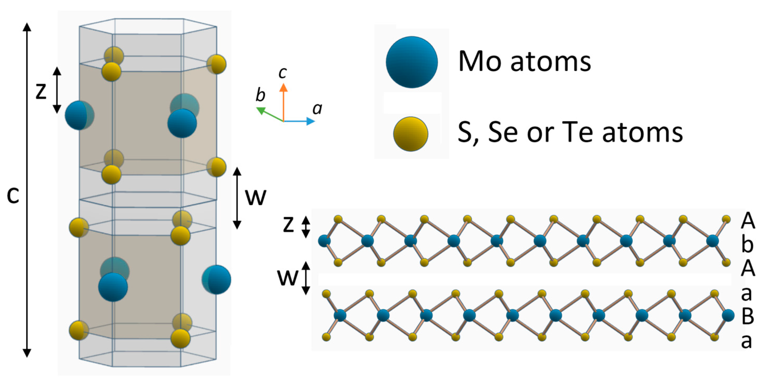
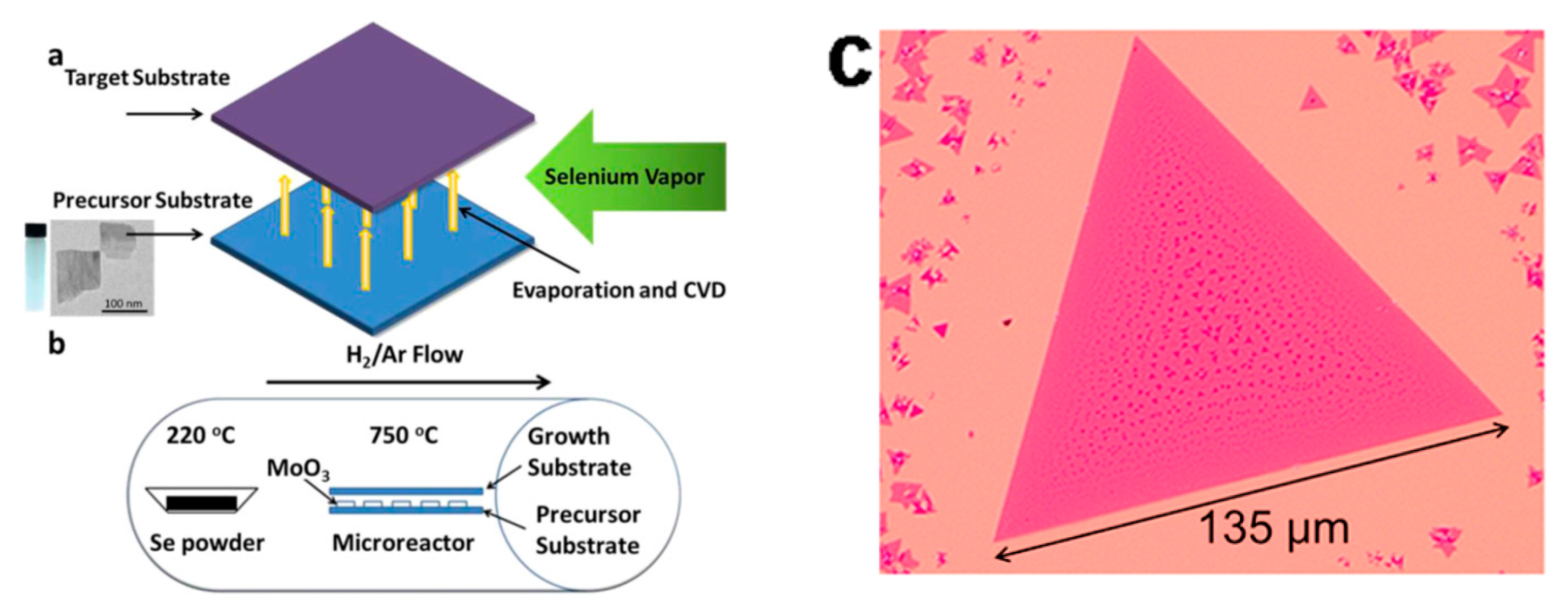
2. Crystalline Structure and Synthesis Techniques
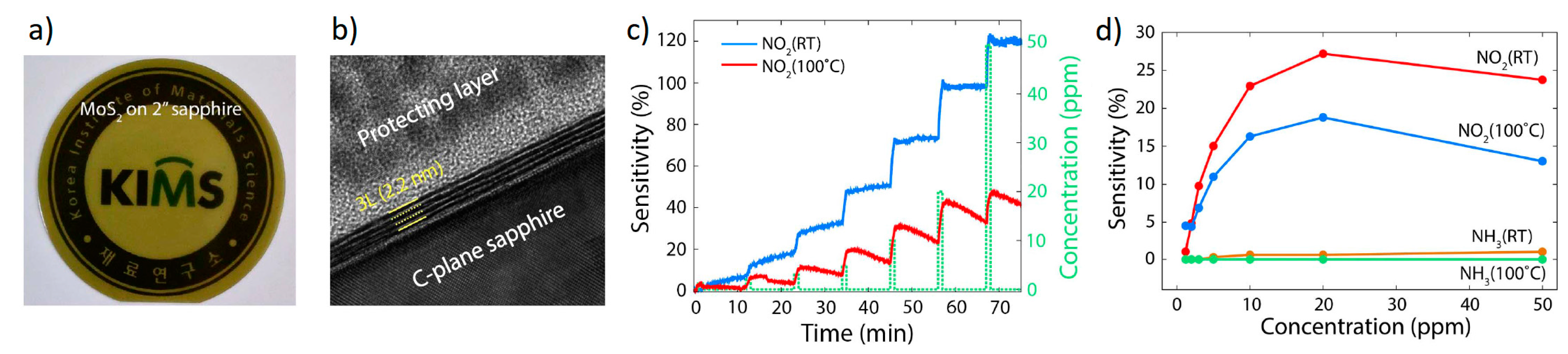
3. Molybdenum Disulfide (MoS2) Chemical Sensors
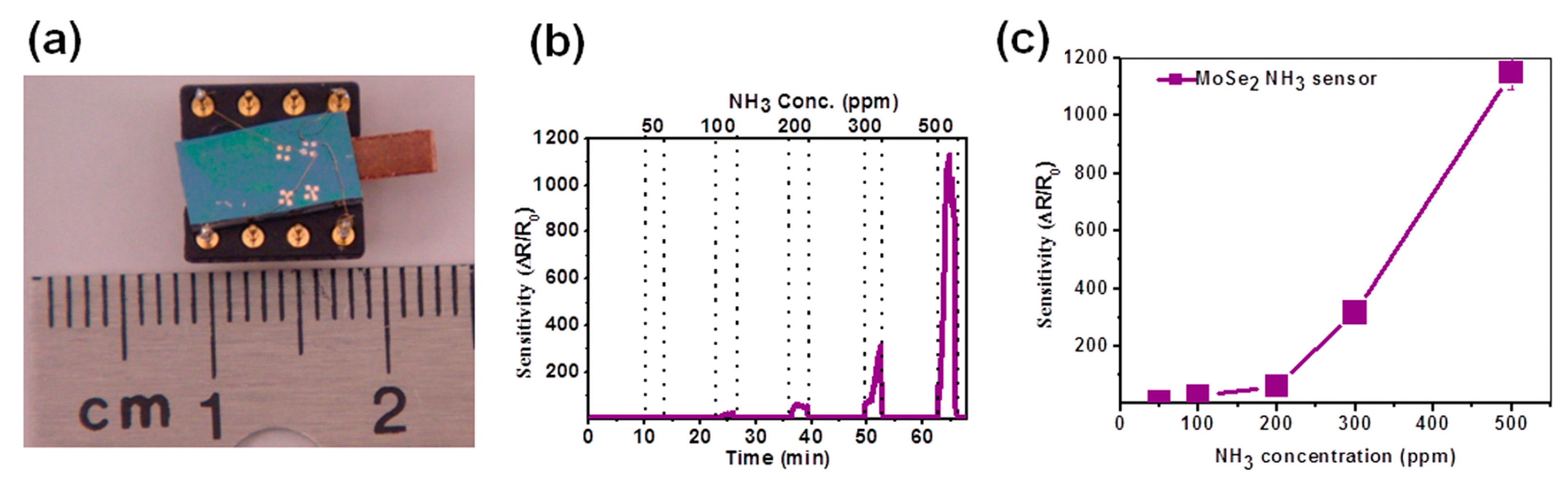
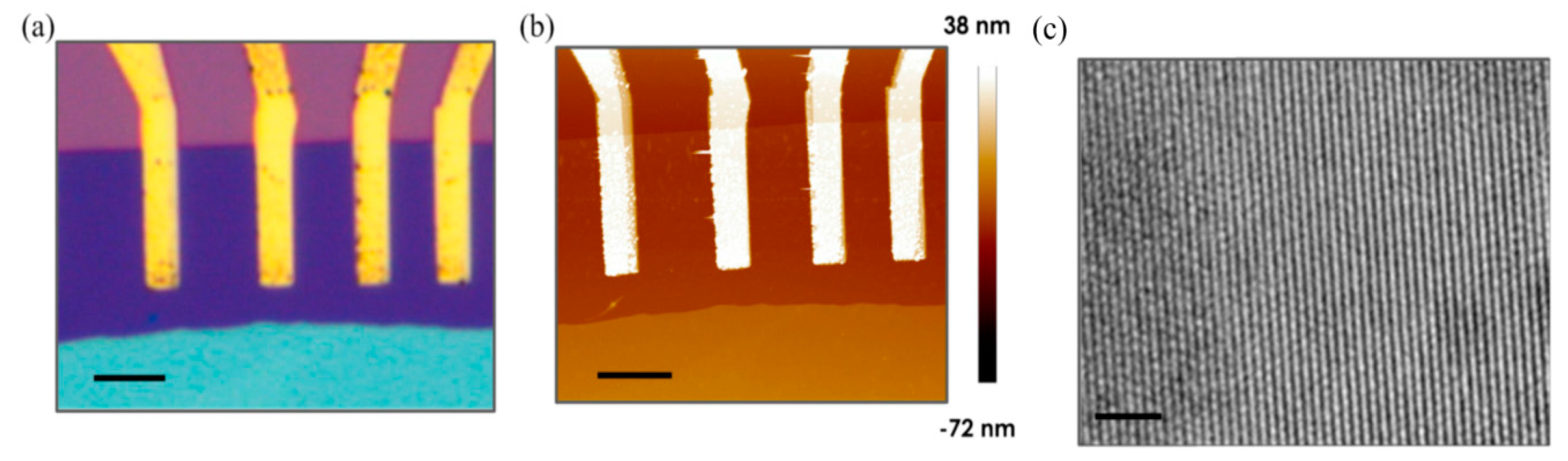
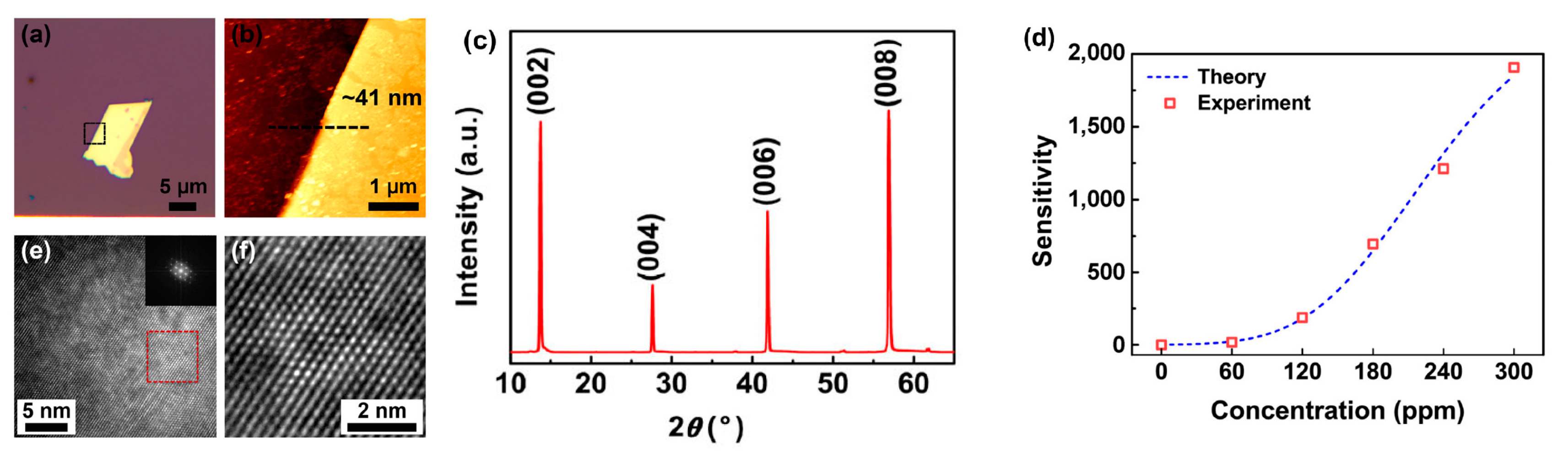
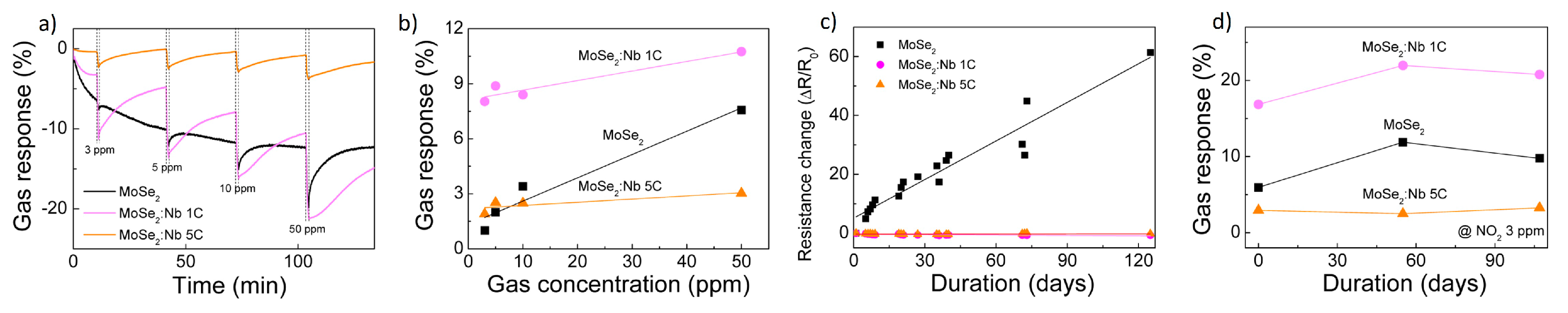
4. Molybdenum Diselenide (MoSe2) Chemical Sensors
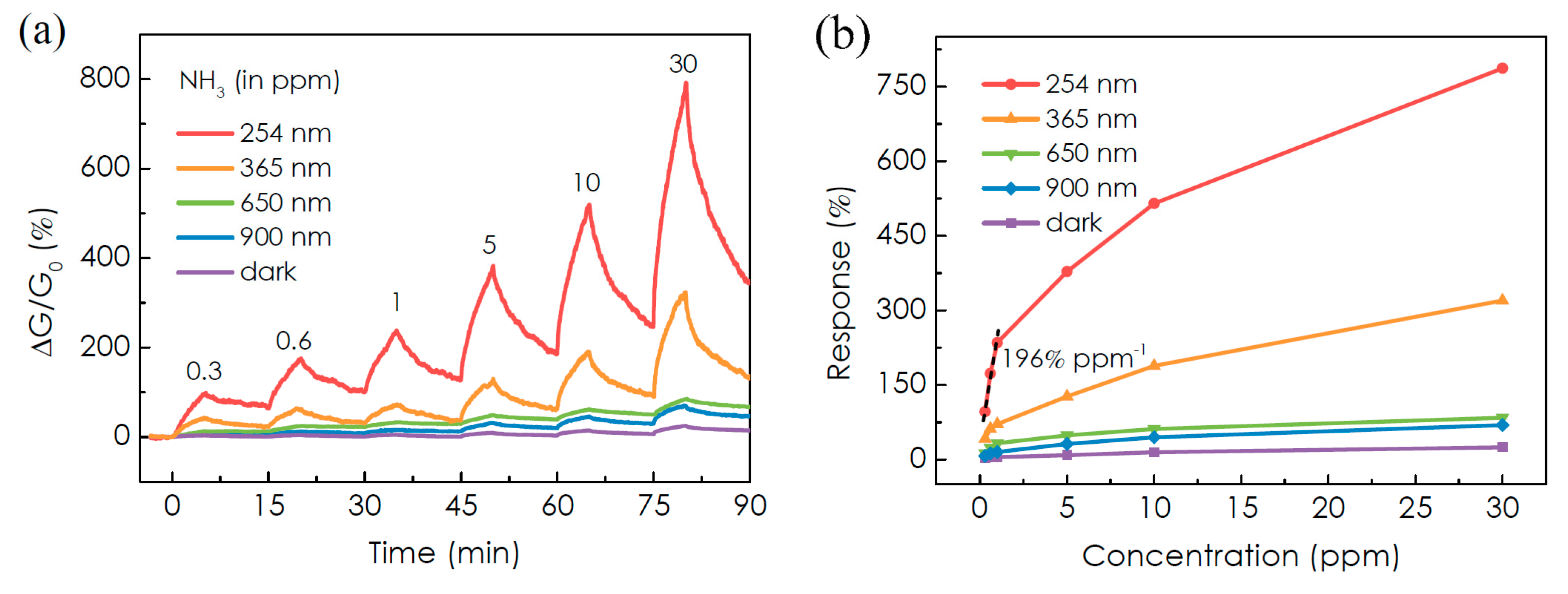
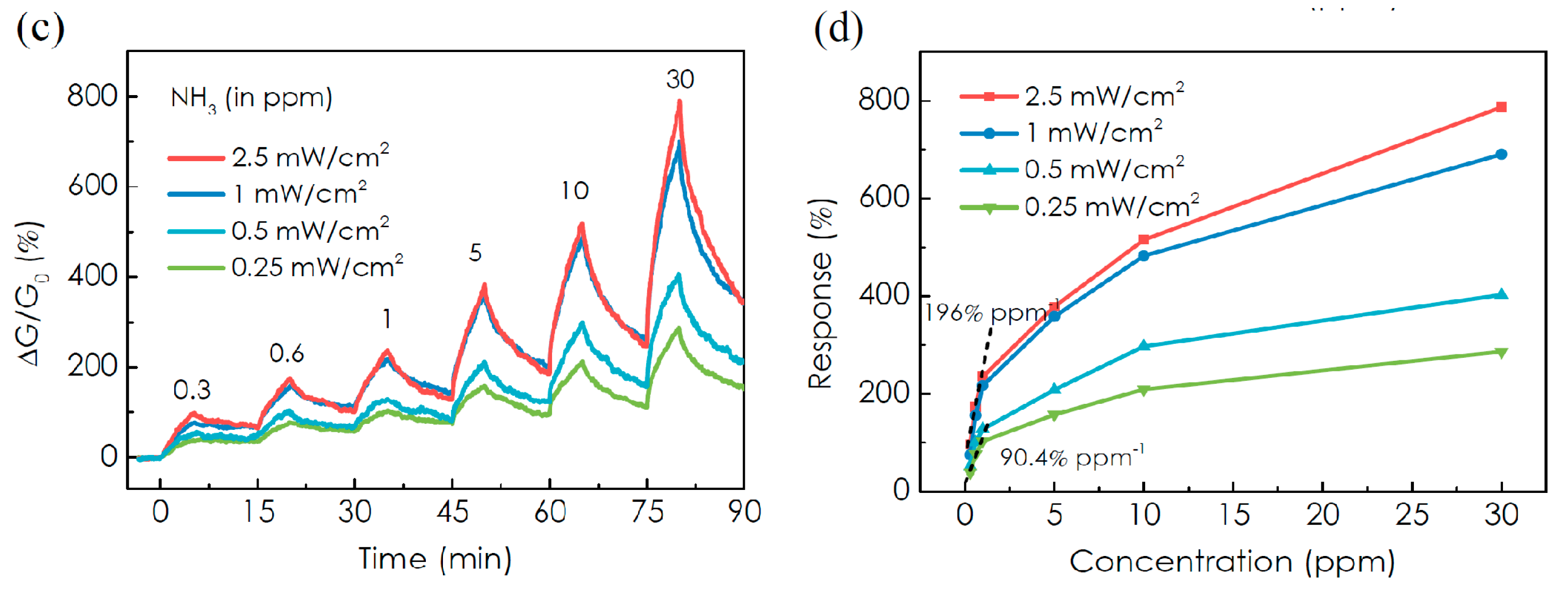
5. Molybdenum Ditellurite (MoTe2) Chemical Sensors
6. Conclusions
Acknowledgments
Author Contributions
Conflicts of Interest
References
- Castro Neto, A.H.; Guinea, F.; Peres, N.M.R.; Novoselov, K.S.; Geim, A.K. The electronic properties of graphene. Rev. Mod. Phys. 2009, 81, 109–162. [Google Scholar] [CrossRef] [Green Version]
- Geim, A.K. Graphene: Status and prospects. Science 2009, 324, 1530–1534. [Google Scholar] [CrossRef] [PubMed]
- Geim, A.K.; Novoselov, K.S. The rise of graphene. Nat. Mater. 2007, 6, 183–191. [Google Scholar] [CrossRef] [PubMed]
- Pinna, N.; Niederberger, M. Surfactant-Free Nonaqueous Synthesis of Metal Oxide Nanostructures. Angew. Chem. Int. Ed. 2008, 47, 5292–5304. [Google Scholar] [CrossRef] [PubMed]
- Devan, R.S.; Patil, R.A.; Lin, J.-H.; Ma, Y.-R. One-dimensional metal-oxide nanostructures: Recent developments in synthesis, characterization, and applications. Adv. Funct. Mater. 2012, 22, 3326–3370. [Google Scholar] [CrossRef]
- Comini, E. Metal oxide nano-crystals for gas sensing. Anal. Chim. Acta 2006, 568, 28–40. [Google Scholar] [CrossRef] [PubMed]
- Chhowalla, M.; Shin, H.S.; Eda, G.; Li, L.; Loh, K.P.; Zhang, H. The chemistry of two-dimensional layered transition metal dichalcogenide nanosheets. Nat. Chem. 2013, 5, 263–275. [Google Scholar] [CrossRef] [PubMed]
- Nobelprize.org. The Official Web Site of the Nobel Prize. Available online: https://www.nobelprize.org/nobel_prizes/physics/laureates/2010/ (accessed on 15 November 2017).
- Cecchel, S.; Chindamo, D.; Turrini, E.; Carnevale, C.; Cornacchia, G.; Gadola, M.; Panvini, A.; Volta, M.; Ferrario, D.; Golimbioschi, R. Impact of reduced mass of light commercial vehicles on fuel consumption, CO2 emissions, air quality, and socio-economic costs. Sci. Total Environ. 2018, 613–614, 409–417. [Google Scholar] [CrossRef] [PubMed]
- Afzal, A.; Cioffi, N.; Sabbatini, L.; Torsi, L. NOx sensors based on semiconducting metal oxide nanostructures: Progress and perspectives. Sens. Actuators B 2012, 171, 25. [Google Scholar] [CrossRef]
- Yuan, W.; Shi, G. Graphene-based gas sensors. J. Mater. Chem. A 2013, 1, 10078–10091. [Google Scholar] [CrossRef]
- Basu, S.; Bhattacharyya, P. Recent developments on graphene and graphene oxide based solid state gas sensors. Sens. Actuators B Chem. 2012, 173, 1–21. [Google Scholar] [CrossRef]
- Chen, X.; McDonald, A.R. Functionalization of Two-Dimensional Transition-Metal Dichalcogenides. Adv. Mater. 2016, 28, 5738–5746. [Google Scholar] [CrossRef] [PubMed]
- Geim, A.K.; Grigorieva, I.V. Van der Waals heterostructures. Nature 2013, 499, 419–425. [Google Scholar] [CrossRef] [PubMed]
- Lévy, F. (Ed.) Crystallography and Crystal Chemistry of Materials with Layered Structures; Springer: Dordrecht, The Netherlands, 1976. [Google Scholar]
- Ramana, C.V.; Becker, U.; Shutthanandan, V.; Julien, C.M. Oxidation and metal-insertion in molybdenite surfaces: Evaluation of charge-transfer mechanisms and dynamics. Geochem. Trans. 2008, 9, 8. [Google Scholar] [CrossRef] [PubMed]
- Vogel, E.M.; Robinson, J.A. Two-dimensional layered transition-metal dichalcogenides for versatile properties and applications. MRS Bull. 2015, 40, 558–563. [Google Scholar] [CrossRef]
- Boker, Th.; Severin, R.; Muller, A.; Janowitz, C.; Manzke, R. Band structure of MoS2, MoSe2, and a-MoTe2: Angle-resolved photoelectron spectroscopy and ab initio calculations. Phys. Rev. B 2001, 64, 235305. [Google Scholar] [CrossRef]
- Parthé, E.; Gmelin, L. Gmelin Handbook of Inorganic and Organometallic Chemsitry; Springer: Berlin, Germany, 1995; Volume B7–B9, p. 16. [Google Scholar]
- Wilson, J.A.; Yoffe, A.D. The transition metal dichalcogenides discussion and interpretation of optical, electrical and structural properties. Adv. Phys. 1969, 18, 193–335. [Google Scholar] [CrossRef]
- Splendiani, A.; Sun, L.; Zhang, Y.; Li, T.; Kim, J.; Chim, C.-Y.; Galli, G.; Wang, F. Emerging photoluminescence in monolayer MoS2. Nano Lett. 2010, 10, 1271–1275. [Google Scholar] [CrossRef] [PubMed]
- Mak, K.F.; Lee, C.; Hone, J.; Shan, J.; Heinz, T.F. Atomically thin MoS2: A new direct-gap semiconductor. Phys. Rev. Lett. 2010, 105, 136805. [Google Scholar] [CrossRef] [PubMed]
- Lin, Y.-C.; Dumcencon, D.O.; Huang, Y.-S.; Suenaga, K. Atomic Mechanism of the Semiconducting-to-Metallic Phase Transition in Single-Layered MoS2. Nat. Nanotechnol. 2014, 9, 391–396. [Google Scholar] [CrossRef] [PubMed]
- Bissessur, R.; Kanatzidis, M.G.; Schindler, J.L.; Kannewurf, C.R. Encapsulation of polymers into MoS2 and metal to insulator transition in metastable MoS2. J. Chem. Soc. Chem. Commun. 1993, 20, 1582–1585. [Google Scholar] [CrossRef]
- Py, M.A.; Haering, R.R. Structural destabilization induced by lithium intercalation in MoS2 and related-compounds. Can. J. Phys. 1983, 61, 76–84. [Google Scholar] [CrossRef]
- Wang, H.; Lu, Z.; Kong, D.; Sun, J.; Hymel, T.M.; Cui, Y. Electrochemical Tuning of MoS2 Nanoparticles on Three-Dimensional Substrate for Efficient Hydrogen Evolution. ACS Nano 2014, 8, 4940–4947. [Google Scholar] [CrossRef] [PubMed]
- Sandoval, S.J.; Yang, D.; Frindt, R.F.; Irwin, J.C. Raman-Study and Lattice-Dynamics of Single Molecular Layers of MoS2. Phys. Rev. B 1991, 44, 3955–3962. [Google Scholar] [CrossRef]
- Naz, M.; Hallam, T.; Berner, N.C.; McEvoy, N.; Gatensby, R.; McManus, J.B.; Akhter, Z.; Duesberg, G.S. A New 2H-2H′/1T Cophase in Polycrystalline MoS2 and MoSe2 Thin Films. ACS Appl. Mater. Interfaces 2016, 8, 31442–31448. [Google Scholar] [CrossRef] [PubMed]
- Lv, R.; Robinson, J.A.; Schaak, R.E.; Sun, D.; Sun, Y.; Mallouk, T.E.; Terrones, M. Transition Metal Dichalcogenides and Beyond: Synthesis, Properties, and Applications of Single- and Few-Layer Nanosheets. Acc. Chem. Res. 2015, 48, 56–64. [Google Scholar] [CrossRef] [PubMed]
- Voiry, D.; Salehi, M.; Silva, R.; Fujita, T.; Chen, M.; Asefa, T.; Shenoy, V.B.; Eda, G.; Chhowalla, M. Conducting MoS2 nanosheets as catalysts for hydrogen evolution reaction. Nano Lett. 2013, 13, 6222–6227. [Google Scholar] [CrossRef] [PubMed]
- McDonnell, S.J.; Wallace, R.M. Atomically-thin layered films for device applications based upon 2D TMDC materials. Thin Solid Films 2016, 616, 482–501. [Google Scholar] [CrossRef]
- Frindt, R.F. Single Crystals of MoS2 Several Molecular Layers Thick. J. Appl. Phys. 1966, 37, 1928. [Google Scholar] [CrossRef]
- Treacy, M.M.J.; Rice, S.B.; Jacobson, A.J.; Lewandowski, J.T. Electron Microscopy Study of Delamination in Dispersions of the Perovskite-Related Layered Phases K[Ca2Nan−3NbnO3n−1]: Evidence for Single-Layer Formation. Chem. Mater. 1990, 2, 279–286. [Google Scholar] [CrossRef]
- Gordon, R.A.; Yang, D.; Crozier, E.D.; Jiang, D.T.; Frindt, R.F. Structures of exfoliated single layers of WS2, MoS2, and MoSe2 in aqueous suspension. Phys. Rev. B 2002, 65, 125407. [Google Scholar] [CrossRef]
- Benavente, E.; Santa Ana, M.A.; Mendizabal, F.; Gonzalez, G. Intercalation chemistry of molybdenum disulfide. Coord. Chem. Rev. 2002, 224, 87–109. [Google Scholar] [CrossRef]
- Joensen, P.; Frindt, R.F.; Morrison, S.R. Single-layer MoS2. Mater. Res. Bull. 1986, 21, 457–461. [Google Scholar] [CrossRef]
- Ambrosi, A.; Sofer, Z.; Pumera, M. Lithium Intercalation Compound Dramatically Influences the Electrochemical Properties of Exfoliated MoS2. Small 2015, 11, 605–612. [Google Scholar] [CrossRef] [PubMed]
- Wypych, F.; Schöllhorn, R. 1T-MoS2, a new metallic modification of molybdenum disulphide. J. Chem. Soc. Chem. Commun. 1992, 19, 1386–1388. [Google Scholar] [CrossRef]
- Eda, G.; Yamaguchi, H.; Voiry, D.; Fujita, T.; Chen, M.; Chhowalla, M. Photoluminescence from chemically exfoliated MoS2. Nano Lett. 2011, 11, 5111–5116. [Google Scholar] [CrossRef] [PubMed]
- Coleman, J.N.; Lotya, M.; O’Neill, A.; Bergin, S.D.; King, P.J.; Khan, U.; Young, K.; Gaucher, A.; De, S.; Smith, R.J.; et al. Two-dimensional nanosheets produced by liquid exfoliation of layered materials. Science 2011, 331, 568–571. [Google Scholar] [CrossRef] [PubMed]
- Lin, Y.C.; Zhang, W.; Huang, J.K.; Liu, K.K.; Lee, Y.H.; Liang, C.T.; Chu, C.W.; Li, L.J. Wafer-scale MoS2 thin layers prepared by MoO3 sulfurization. Nanoscale 2012, 4, 6637–6641. [Google Scholar] [CrossRef] [PubMed]
- Mercier, J. Recent developments in chemical vapor transport in closed tubes. J. Cryst. Growth 1982, 56, 235. [Google Scholar] [CrossRef]
- Al-Hilli, A.A.; Evans, B.L. The preparation and properties of transition metal dichalcogenide single crystals. J. Cryst. Growth 1972, 15, 93. [Google Scholar] [CrossRef]
- Wu, S.; Huang, C.; Aivazian, G.; Ross, J.S.; Cobden, D.H.; Xu, X. Vapor-solid growth of high optical quality MoS2 monolayers with near-unity valley polarization. ACS Nano 2013, 7, 2768–2772. [Google Scholar] [CrossRef] [PubMed]
- Yu, Y.; Li, C.; Liu, Y.; Su, L.; Zhang, Y.; Cao, L. Controlled Scalable Synthesis of Uniform, High-Quality Monolayer and Few-layer MoS2 Films. Sci. Rep. 2013, 3, 1866. [Google Scholar] [CrossRef] [PubMed]
- Koma, A.; Yoshimura, K. Ultrasharp interfaces grown with Van der Waals epitaxy. Surf. Sci. 1986, 174, 556–560. [Google Scholar] [CrossRef]
- Ueno, K.; Shimada, T.; Saiki, K.; Koma, A. Heteroepitaxial growth of layered transition metal dichalcogenides on sulfur-terminated GaAs {111} surfaces. Appl. Phys. Lett. 1990, 56, 327–329. [Google Scholar] [CrossRef]
- Krustok, J.; Raadik, T.; Jaaniso, R.; Kiisk, V.; Sildos, I.; Marandi, M.; Komsa, H.-P.; Li, B.; Zhang, X.; Gong, Y.; et al. Optical study of local strain related disordering in CVD-grown MoSe2 monolayers. Appl. Phys. Lett. 2016, 109, 253106. [Google Scholar] [CrossRef]
- Ahn, J.-H.; Parkin, W.M.; Naylor, C.H.; Johnson, A.T.C.; Drndić, M. Ambient effects on electrical characteristics of CVD-grown monolayer MoS2 field-effect transistors. Sci. Rep. 2017, 7, 4075. [Google Scholar] [CrossRef] [PubMed]
- Hadouda, H.; Pouzet, J.; Bernede, J.C.; Barreau, A. MoS2 thin film synthesis by soft sulfurization of a molybdenum layer. Mater. Chem. Phys. 1995, 42, 291. [Google Scholar] [CrossRef]
- Huang, Y.; Guo, J.; Kang, Y.; Ai, Y.; Li, C.M. Two dimensional atomically thin MoS2 nanosheets and their sensing applications. Nanoscale 2015, 7, 19358. [Google Scholar] [CrossRef] [PubMed]
- Wang, Y.-H.; Huang, K.-J.; Wu, X. Recent advances in transition-metal dichalcogenides based electrochemical biosensors: A review. Biosens. Bioelectron. 2017, 97, 305–316. [Google Scholar] [CrossRef] [PubMed]
- Wang, L.; Xiong, Q.; Xiao, F.; Duan, H. 2D nanomaterials based electrochemical biosensors for cancer diagnosis. Biosens. Bioelectron. 2017, 89, 136–151. [Google Scholar] [CrossRef] [PubMed]
- Perkins, F.K.; Friedman, A.L.; Cobas, E.; Campbell, P.M.; Jernigan, G.G.; Jonker, B.T. Chemical Vapor Sensing with Monolayer MoS2. Nano Lett. 2013, 13, 668–673. [Google Scholar] [CrossRef] [PubMed]
- Friedman, A.L.; Perkins, F.K.; Cobas, E.; Jernigan, G.G.; Campbell, P.M.; Hanbicki, A.T.; Jonker, B.T. Chemical vapor sensing of two-dimensional MoS2 field effect transistor devices. Solid-State Electron. 2014, 101, 2–7. [Google Scholar] [CrossRef]
- Friedman, A.L.; Perkins, F.K.; Hanbicki, A.T.; Culbertson, J.C.; Campbell, P.M. Dynamics of chemical vapor sensing with MoS2 using 1T/2H phase contacts/channel. Nanoscale 2016, 8, 11445. [Google Scholar] [CrossRef] [PubMed]
- Li, W.; Xu, H.; Zhai, T.; Yu, H.; Chen, Z.; Qiu, Z.; Song, X.; Wang, J.; Cao, B. Enhanced triethylamine sensing properties by designingAu@SnO2/MoS2 nanostructure directly on alumina tubes. Sens. Actuators B 2017, 253, 97–107. [Google Scholar] [CrossRef]
- Cho, B.; Hahm, M.G.; Choi, M.; Yoon, J.; Kim, A.R.; Lee, Y.-J.; Park, S.-G.; Kwon, J.-D.; Kim, C.S.; Song, M.; et al. Charge-transfer-based Gas Sensing Using Atomic-layer MoS2. Sci. Rep. 2015, 5, 8052. [Google Scholar] [CrossRef] [PubMed]
- Cho, B.; Kim, A.R.; Park, Y.; Yoon, J.; Lee, Y.-J.; Lee, S.; Yoo, T.J.; Kang, C.G.; Lee, B.H.; Ko, H.C.; et al. Bifunctional Sensing Characteristics of Chemical Vapor Deposition Synthesized Atomic-Layered MoS2. ACS Appl. Mater. Interfaces 2015, 7, 2952–2959. [Google Scholar] [CrossRef] [PubMed]
- Dolui, K.; Rungger, I.; Sanvito, S. Origin of the n-type and p-type conductivity of MoS2 monolayers on a SiO2 substrate. Phys. Rev. B 2013, 87, 165402. [Google Scholar] [CrossRef]
- Late, D.J.; Huang, Y.-K.; Liu, B.; Acharya, J.; Shirodkar, S.N.; Luo, J.; Yan, A.; Charles, D.; Waghmare, U.V.; Dravid, V.P.; et al. Sensing Behavior of Atomically Thin-Layered MoS2 Transistors. ACS Nano 2013, 7, 4879–4891. [Google Scholar] [CrossRef] [PubMed]
- Zhang, D.; Sun, Y.; Li, P.; Zhang, Y. Facile Fabrication of MoS2-Modified SnO2 Hybrid Nanocomposite for Ultrasensitive Humidity Sensing. ACS Appl. Mater. Interfaces 2016, 8, 14142–14149. [Google Scholar] [CrossRef] [PubMed]
- Tan, Y.; Yu, K.; Yang, T.; Zhang, Q.; Cong, W.; Yin, H.; Zhang, Z.; Chen, Y.; Zhu, Z. The combinations of hollow MoS2 micro@nanospheres: One-step synthesis, excellent photocatalytic and humidity sensing properties. J. Mater. Chem. C 2014, 2, 5422. [Google Scholar] [CrossRef]
- Li, N.; Chen, X.-D.; Chen, X.-P.; Ding, X.; Zhao, X. Ultra-High Sensitivity Humidity Sensor Based on MoS2/Ag Composite Films. IEEE Electron Device Lett. 2017, 38. [Google Scholar] [CrossRef]
- Liu, B.; Chen, L.; Liu, G.; Abbas, A.N.; Fathi, M.; Zhou, C. High-Performance Chemical Sensing Using Schottky-Contacted Chemical Vapor Deposition Grown Monolayer MoS2 Transistors. ACS Nano 2014, 8, 5304–5314. [Google Scholar] [CrossRef] [PubMed]
- Donarelli, M.; Prezioso, S.; Perrozzi, F.; Bisti, F.; Nardone, M.; Giancaterini, L.; Cantalini, C.; Ottaviano, L. Response to NO2 and other gases of resistive chemically exfoliated MoS2-based gas sensors. Sens. Actuators B 2015, 207, 602–613. [Google Scholar] [CrossRef]
- Lu, J.; Lu, J.H.; Liu, H.; Liu, B.; Gong, L.; Tok, E.S.; Loh, K.P.; Sow, C.H. Microlandscaping of Au Nanoparticles on Few-Layer MoS2 Films for Chemical Sensing. Small 2015, 11, 1792–1800. [Google Scholar] [CrossRef] [PubMed]
- Baek, D.-H.; Kim, J. MoS2 gas sensor functionalized by Pd for the detection of hydrogen. Sens. Actuators B 2017, 250, 686–691. [Google Scholar] [CrossRef]
- Liu, Y.; Hao, L.; Gao, W.; Xue, Q.; Guo, W.; Wu, Z.; Lin, Y.; Zeng, H.; Zhu, J.; Zhang, W. Electrical characterization and ammonia sensing properties of MoS2/Si p–n junction. J. Alloys Compd. 2015, 631, 105–110. [Google Scholar] [CrossRef]
- Liu, Y.; Hao, L.; Gao, W.; Wu, Z.; Lin, Y.; Li, G.; Guo, W.; Yu, L.; Zeng, H.; Zhu, J.; et al. Hydrogen gas sensing properties of MoS2/Si heterojunction. Sens. Actuators B 2015, 211, 537–543. [Google Scholar] [CrossRef]
- Yan, H.; Song, P.; Zhang, S.; Yang, Z.; Wang, Q. Facile synthesis, characterization and gas sensing performance of ZnO nanoparticles-coated MoS2 nanosheets. J. Alloys Compd. 2016, 662, 118–125. [Google Scholar] [CrossRef]
- Yu, L.; Guo, F.; Liu, S.; Qi, J.; Yin, M.; Yang, B.; Liu, Z.; Fan, X.H. Hierarchical 3D flower-like MoS2 spheres: Post-thermal treatment in vacuum and their NO2 sensing properties. Mater. Lett. 2016, 183, 122–126. [Google Scholar] [CrossRef]
- Dwivedi, P.; Das, S.; Dhanekar, S. Wafer-Scale Synthesized MoS2/Porous Silicon Nanostructures for Efficient and Selective Ethanol Sensing at Room Temperature. ACS Appl. Mater. Interfaces 2017, 9, 21017–21024. [Google Scholar] [CrossRef] [PubMed]
- Yue, N.; Weicheng, J.; Rongguo, W.; Guomin, D.; Yifan, H. Hybrid nanostructures combining graphene-MoS2 quantum dots for gas sensing. J. Mater. Chem. A 2016, 4, 8198. [Google Scholar] [CrossRef]
- Buscema, M.; Barkelid, M.; Zwiller, V.; van der Zant, H.S.; Steele, G.A.; Castellanos-Gomez, A. Large and Tunable Photothermoelectric Effect in Single-Layer MoS2. Nano Lett. 2013, 13, 358–363. [Google Scholar] [CrossRef] [PubMed]
- Lim, S.; Cho, B.; Bae, J.; Kim, A.R.; Lee, K.H.; Kim, S.H.; Hahm, M.G.; Nam, J. Electrohydrodynamic printing for scalable MoS2 flake coating: Application to gas sensing device. Nanotechnology 2016, 27, 435501–435509. [Google Scholar] [CrossRef] [PubMed]
- Yan, H.; Song, P.; Zhang, S.; Yang, Z.; Wang, Q. Dispersed SnO2 nanoparticles on MoS2 nanosheets for superior gas-sensing performances to ethanol. RSC Adv. 2015, 5, 79593. [Google Scholar] [CrossRef]
- Cui, S.; Wen, Z.; Huang, X.; Chang, J.; Chen, J. Stabilizing MoS2 Nanosheets through SnO2 Nanocrystal Decoration for High-Performance Gas Sensing in Air. Small 2015, 11, 2305–2313. [Google Scholar] [CrossRef] [PubMed]
- Zhao, P.X.; Tang, Y.; Mao, J.; Chen, Y.X.; Song, H.; Wang, J.W.; Song, Y.; Liang, Y.Q.; Zhang, X.M. One-Dimensional MoS2-Decorated TiO2 nanotube gas sensors for efficient alcohol sensing. J. Alloys Compd. 2016, 674, 252–258. [Google Scholar] [CrossRef]
- Zhou, Y.; Liu, G.; Zhu, X.; Guo, Y. Ultrasensitive NO2 gas sensing based on rGO/MoS2 nanocompositefilm at low temperature. Sens. Actuators B 2017, 251, 280–290. [Google Scholar] [CrossRef]
- He, Q.; Zeng, Z.; Yin, Z.; Li, H.; Wu, S.; Huang, X.; Zhang, H. Fabrication of Flexible MoS2 Thin-Film Transistor Arrays for Practical Gas-Sensing Applications. Small 2012, 8, 2994–2999. [Google Scholar] [CrossRef] [PubMed]
- Jariwala, D.; Sangwan, V.K.; Lauhon, L.J.; Marks, T.J.; Hersam, M.C. Emerging Device Applications for Semiconducting Two-Dimensional Transition Metal Dichalcogenides. ACS Nano 2014, 8, 1102. [Google Scholar] [CrossRef] [PubMed]
- Ouyang, T.; Lin, L.; Xia, K.; Jiang, M.; Lang, Y.; Guan, H.; Yu, J.; Li, D.; Chen, G.; Zhu, W.; et al. Enhanced optical sensitivity of molybdenum diselenide (MoSe2) coated side polished fiber for humidity sensing. Opt. Express 2017, 25, 9823–9833. [Google Scholar] [CrossRef] [PubMed]
- Shaw, J.C.; Zhou, H.; Chen, Y.; Weiss, N.O.; Liu, Y.; Huang, Y.; Duan, X. Chemical vapor deposition growth of monolayer MoSe2 nanosheets. Nano Res. 2014, 7, 511–517. [Google Scholar] [CrossRef]
- O’Brien, M.; McEvoy, N.; Hanlon, D.; Lee, K.; Gatensby, R.; Coleman, J.N.; Duesberg, G.S. Low wavenumber Raman spectroscopy of highly crystalline MoSe2 grown by chemical vapor deposition. Phys. Status Solidi B 2015, 252, 2385–2389. [Google Scholar] [CrossRef]
- Wang, X.; Gong, Y.; Shi, G.; Chow, W.L.; Keyshar, K.; Ye, G.; Vajtai, R.; Lou, J.; Liu, Z.; Ringe, E.; et al. Chemical Vapor Deposition Growth of Crystalline Monolayer MoSe2. ACS Nano 2014, 8, 5125–5131. [Google Scholar] [CrossRef] [PubMed]
- Onomitsu, K.; Krajewska, A.; Neufeld, R.A.E.; Maeda, F.; Kumakura, K.; Yamamoto, H. Epitaxial growth of monolayer MoSe2 on GaAs. Appl. Phys. Express 2016, 9, 115501. [Google Scholar] [CrossRef]
- Late, D.J.; Doneux, T.; Bougouma, M. Single-layer MoSe2 based NH3 gas sensor. Appl. Phys. Lett. 2014, 105, 233103. [Google Scholar] [CrossRef]
- Baek, J.; Yin, D.; Liu, N.; Omkaram, I.; Jung, C.; Im, H.; Hong, S.; Kim, S.M.; Hong, Y.K.; Hur, J.; et al. A highly sensitive chemical gas detecting transistor based on highly crystalline CVD-grown MoSe2 films. Nano Res. 2017, 10, 1861–1871. [Google Scholar] [CrossRef]
- Standards-Air Quality-Environment-European Commission. Available online: http://ec.europa.eu/environment/air/quality/standards.htm (accessed on 15 November 2017).
- The National Institute for Occupational Safety and Health (NIOSH). Available online: https://www.cdc.gov/niosh/idlh/10102440.html (accessed on 15 November 2017).
- Choi, S.Y.; Kim, Y.; Chung, H.-S.; Kim, A.R.; Kwon, J.-D.; Park, J.; Kim, Y.L.; Kwon, S.-H.; Hahm, M.G.; Cho, B. Effect of Nb Doping on Chemical Sensing Performance of Two-Dimensional Layered MoSe2. ACS Appl. Mater. Interfaces 2017, 9, 3817–3823. [Google Scholar] [CrossRef] [PubMed]
- Kim, A.R.; Kim, Y.; Nam, J.; Chung, H.-S.; Kim, D.-H.J.; Kwon, J.-D.; Park, S.W.; Park, J.J.H.; Choi, S.Y.M.; Lee, B.H.; et al. Alloyed 2D Metal-Semiconductor Atomic Layer Junctions. Nano Lett. 2016, 16, 1890–1895. [Google Scholar] [CrossRef] [PubMed]
- Fathipour, S.; Ma, N.; Hwang, W.S.; Protasenko, V.; Vishwanath, S.; Xing, H.G.; Xu, H.; Jena, D.; Appenzeller, J.; Seabaugh, A. Exfoliated multilayer MoTe2 field-effect transistors. Appl. Phys. Lett. 2014, 105, 192101–192103. [Google Scholar] [CrossRef]
- Abruña, H.D.; Hope, G.A.; Bard, A.J. Semiconductor Electrodes XLV. Photoelectrochemistry of n- and p-Type MoTe2 in Aqueous Solutions. J. Electrochem. Soc. 1982, 129, 2224–2228. [Google Scholar] [CrossRef]
- Conan, A.; Bonnet, A.; Zoaeter, M.; Ramoul, D. Dependence of the Total Mobility in a One-Band Model Applicationto n-Type MoTe2. Phys. Status Solidi B 1984, 124, 403–410. [Google Scholar] [CrossRef]
- Bernede, J.C.; Kettaf, M.; Khelil, A.; Spiesser, M. p-n junctions in molybdenum ditelluride. Phys. Status Solidi A 1996, 157, 205–209. [Google Scholar] [CrossRef]
- Chang, Y.-M.; Lin, C.-Y.; Lin, Y.-F.; Tsukagoshi, K. Two-dimensional MoTe2 materials: From synthesis, identification, and charge transport to electronics applications. Jpn. J. Appl. Phys. 2016, 55, 1102A1. [Google Scholar] [CrossRef]
- Lin, Y.-F.; Xu, Y.; Wang, S.-T.; Li, S.-L.; Yamamoto, M.; Aparecido-Ferreira, M.; Li, H.; Sun, W.; Nakaharai, S.; Jian, W.-B.; et al. Ambipolar MoTe2 Transistors and Their Applications in Logic Circuits. Adv. Mater. 2014, 26, 3263. [Google Scholar] [CrossRef] [PubMed]
- Vellinga, M.B.; Jonge, R.D.; Haas, C. Semiconductor to metal transition in MoTe2. J. Solid State Chem. 1970, 2, 299–302. [Google Scholar] [CrossRef]
- Kim, H.-J.; Kang, S.-H.; Hamada, I.; Son, Y.-W. Origins of the structural phase transitions in MoTe2 and WTe2. Phys. Rev. B 2017, 95, 180101(R). [Google Scholar] [CrossRef]
- Yamamoto, M.; Wang, S.T.; Ni, M.; Lin, Y.-F.; Li, S.-L.; Aikawa, S.; Jian, W.B.; Ueno, K.; Wakabayashi, K.; Tsukagoshi, K. Strong Enhancement of Raman Scattering from a Bulk-Inactive Vibrational Mode in Few-Layer MoTe2. ACS Nano 2014, 8, 3895–3903. [Google Scholar] [CrossRef] [PubMed]
- Qi, Y.; Naumov, P.G.; Ali, M.N.; Rajamathi, C.R.; Schnelle, W.; Barkalov, O.; Hanfland, M.; Wu, S.C.; Shekhar, C.; Sun, Y.; et al. Superconductivity in Weyl Semimetal Candidate MoTe2. Nat. Commun. 2016, 7, 11038. [Google Scholar] [CrossRef] [PubMed]
- Chen, F.C.; Luo, X.; Xiao, R.C.; Lu, W.J.; Zhang, B.; Yang, H.X.; Li, J.Q.; Pei, Q.L.; Shao, D.F.; Zhang, R.R.; et al. Superconductivity Enhancement in the S-doped Weyl Semimetal Candidate MoTe2. Appl. Phys. Lett. 2016, 108, 162601. [Google Scholar] [CrossRef]
- Cheng, S.; Yang, L.; Li, J.; Liu, Z.; Zhang, W.; Chang, H. Large area, phase-controlled growth of few-layer, two-dimensional MoTe2 and lateral 1T′–2H heterostructures by chemical vapor deposition. CrystEngComm 2017, 19, 1045–1051. [Google Scholar] [CrossRef]
- Yang, L.; Zhang, W.; Li, J.; Cheng, S.; Xie, Z.; Chang, H. Tellurization Velocity-Dependent Metallic—Semiconducting—Metallic Phase Evolution in Chemical Vapor Deposition Growth of Large-Area, Few-Layer MoTe2. ACS Nano 2017, 11, 1964–1972. [Google Scholar] [CrossRef] [PubMed]
- Diaz, H.C.; Chaghi, R.; Ma, Y.; Batzill, M. Molecular beam epitaxy of the van der Waals heterostructure MoTe2 on MoS2: Phase, thermal, and chemical stability. 2D Mater. 2015, 2, 044010. [Google Scholar] [CrossRef]
- Mirabelli, G.; McGeough, C.; Schmidt, M.; McCarthy, E.K.; Monaghan, S.; Povey, I.M.; McCarthy, M.; Gity, F.; Nagle, R.; Hughes, G.; et al. Air sensitivity of MoS2, MoSe2, MoTe2, HfS2, and HfSe2. J. Appl. Phys. 2016, 120, 125102. [Google Scholar] [CrossRef]
- Lin, Y.-F.; Xu, Y.; Lin, C.-Y.; Suen, Y.-W.; Yamamoto, M.; Nakaharai, S.; Ueno, K.; Tsukagoshi, K. Origin of Noise in Layered MoTe2 Transistors and its Possible Use for Environmental Sensors. Adv. Mater. 2015, 27, 6612–6619. [Google Scholar] [CrossRef] [PubMed]
- Feng, Z.; Xie, Y.; Chen, J.; Yu, Y.; Zheng, S.; Zhang, R.; Li, Q.; Chen, X.; Sun, C.; Zhang, H.; et al. Highly sensitive MoTe2 chemical sensor with fast recovery rate through gate biasing. 2D Mater. 2017, 4, 025018. [Google Scholar] [CrossRef]
- Gao, X.P.A.; Zheng, G.; Lieber, C.M. Subthreshold regime has the optimal sensitivity for nanowire FET biosensors. Nano Lett. 2010, 10, 547–552. [Google Scholar] [CrossRef] [PubMed]
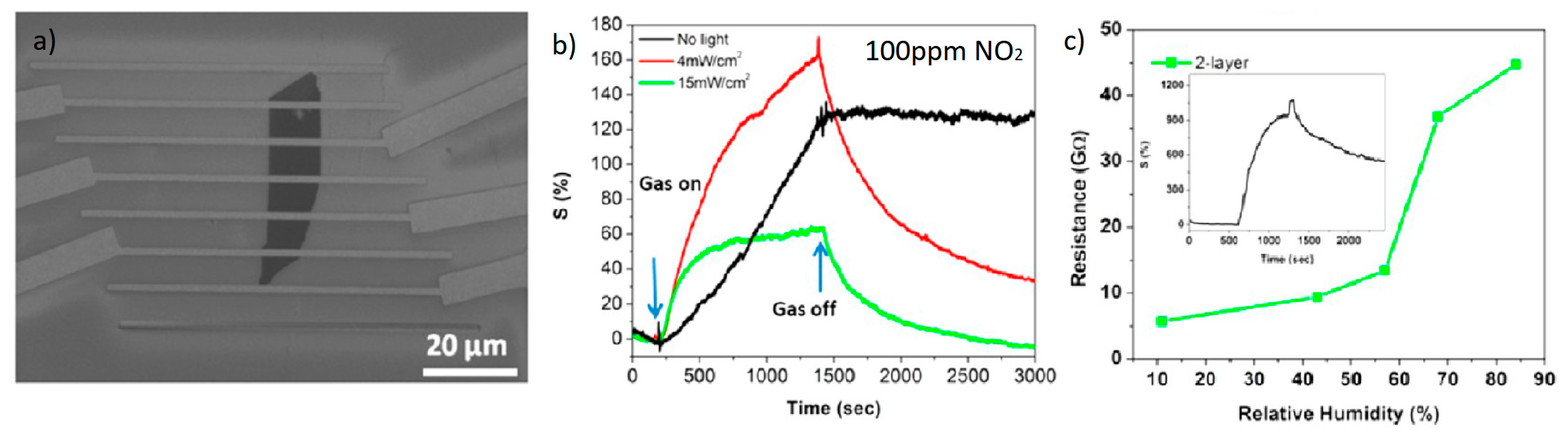
- Feng, Z.; Xie, Y.; Wu, E.; Yu, Y.; Zheng, S.; Zhang, R.; Chen, X.; Sun, C.; Zhang, H.; Pang, W.; et al. Enhanced Sensitivity of MoTe2 Chemical Sensor through Light Illumination. Micromachines 2017, 8, 155. [Google Scholar] [CrossRef]
- Neri, G. Thin 2D: The New Dimensionality in Gas Sensing. Chemosensors 2017, 5, 21. [Google Scholar] [CrossRef]
- Cho, S.-Y.; Lee, Y.; Koh, H.J.; Jung, H.; Kim, J.-S.; Yoo, H.-W.; Kim, J.; Jung, H.-T. Superior Chemical Sensing Performance of Black Phosphorus: Comparison with MoS2 and Graphene. Adv. Mater. 2016, 28, 7020–7028. [Google Scholar] [CrossRef] [PubMed]
- Samnakay, R.; Jiang, C.; Rumyantsev, S.L.; Shur, M.S.; Balandin, A.A. Selective chemical vapor sensing with few-layer MoS2 thin-film transistors: Comparison with graphene devices. Appl. Phys. Lett. 2015, 106, 023115. [Google Scholar] [CrossRef]


| MoS2 | MoSe2 | MoTe2 | |
|---|---|---|---|
| a [Å] | 3.160 | 3.299 | 3.522 |
| c [Å] | 12.294 | 12.938 | 13.968 |
| 2z [Å] | 3.172 | 3.338 | 3.604 |
| w [Å] | 2.975 | 3.131 | 3.380 |
| c/a [Å] | 3.891 | 3.922 | 3.966 |
| Indirect Bandgap [eV] | 1.29 | 1.10 | 1.00 |
| Direct Bandgap [eV] | 1.78 | 1.42 | 1.00 |
| Ref. | Material | Growth Technique | Device Type | Gas and Temperature | Performances |
|---|---|---|---|---|---|
| [58] | MoS2 | CVD | Resistive | NH3-RT NO2-RT | <2%@20ppm ≈27%@20ppm |
| [59] | MoS2 | CVD | Resistive | NO2-RT | ≈120%@1ppm 1 |
| [61] | MoS2 | Mechanical Exfoliation | FET | NH3-RT NO2-RT | ≈50%@200ppm 1 ≈400%@20ppm 1 |
| [65] | MoS2 | CVD | FET | NH3-RT NO2-RT | ≈50%@200ppm 2 ≈50%@100ppb 2 |
| [66] | MoS2 | Liquid Exfoliation | Resistive | NO2-200 °C | 5.8@1ppm |
| [68] | MoS2 + Pd NPs | Drop Casting + Evaporation | Resistive | H2-RT | ≈35%@1% |
| [69,70] | MoS2/Si | Magnetron Sputtering | Resistive pn junction | NH3-RT H2-RT | ≈300%@50ppm 15.4%@5000ppm 3 |
| [71] | MoS2 + ZnO | Hydrothermal | Resistive | Ethanol-260 °C | 42.8@50ppm |
| [72] | MoS2 | Hydrothermal | Resistive | NO2-150 °C | 78%@50ppm |
| [73] | MoS2 Porous | Sputtering + Film Conversion | Resistive | Ethanol-RT | ≈2%@1ppm 1 |
| [74] | MoS2/GO QDs | Exfoliation + Sonication | Resistive | NO2-RT NH3-RT | ≈35%@10ppm 1 ≈20%@10ppm 1 |
| [76] | MoS2 Flakes | Sonication | Resistive | NO2-100 °C CNH3-100 °C | ≈10%@10ppm 1 ≈35%@10ppm 1 |
| [77] | SnO2@MoS2 | Hydrothermal | Resistive | Ethanol-280 °C | ≈50@50ppm |
| [78] | SnO2@MoS2 | Hydrothermal | FET | NO2-RT | ≈28%@10ppm |
| [79] | MoS2@TiO2 | Hydrothermal | Resistive | Ethanol-150 °C | 14.2@100ppm 4 |
| [80] | MoS2/rGO | Hydrothermal | Resistive | NO2-RT | ≈60%@2ppm |
| [81] | MoS2 | Liquid Exfoliation | FET | NO2-RT | ≈11%@1ppm 1 |
| Ref. | Material | Growth Technique | Device Type | Gas and Temperature | Performances |
|---|---|---|---|---|---|
| [88] | MoSe2 | Mechanical Exfoliation | Resistive/FET | NH3-RT | ≈200@200ppm 1 |
| [89] | MoSe2 | CVD + Mechanical Exfoliation | Resistive/FET | NO2-RT | 1907@300ppm 2 |
| [92] | Nb-doped MoSe2 | ALD + Film Conversion | Resistive | NO2-150 °C | 8%@3ppm 2 |
| Ref. | Material | Growth Technique | Device Type | Gas and Temperature | Performances |
|---|---|---|---|---|---|
| [109] | MoTe2 | Mechanical Exfoliation | FET | Air | - |
| [110] | MoTe2 | Exfoliation | FET | NO2-RT NH3-RT | 140%@100ppb * ≈30%@2ppm * |
| [112] | MoTe2 | Mechanical Exfoliation | FET + Light Illumination | NH3-RT | 100%@300ppb * |
© 2017 by the author. Licensee MDPI, Basel, Switzerland. This article is an open access article distributed under the terms and conditions of the Creative Commons Attribution (CC BY) license (http://creativecommons.org/licenses/by/4.0/).
Share and Cite
Zappa, D. Molybdenum Dichalcogenides for Environmental Chemical Sensing. Materials 2017, 10, 1418. https://doi.org/10.3390/ma10121418
Zappa D. Molybdenum Dichalcogenides for Environmental Chemical Sensing. Materials. 2017; 10(12):1418. https://doi.org/10.3390/ma10121418
Chicago/Turabian StyleZappa, Dario. 2017. "Molybdenum Dichalcogenides for Environmental Chemical Sensing" Materials 10, no. 12: 1418. https://doi.org/10.3390/ma10121418
APA StyleZappa, D. (2017). Molybdenum Dichalcogenides for Environmental Chemical Sensing. Materials, 10(12), 1418. https://doi.org/10.3390/ma10121418