The modeling and control design of the distributed converters in a standalone DC microgrid will be discussed from two aspects: device-regulating mode and bus-regulating mode.
3.1. Closed-Loop Input Impedance of the Device-Regulating Converters
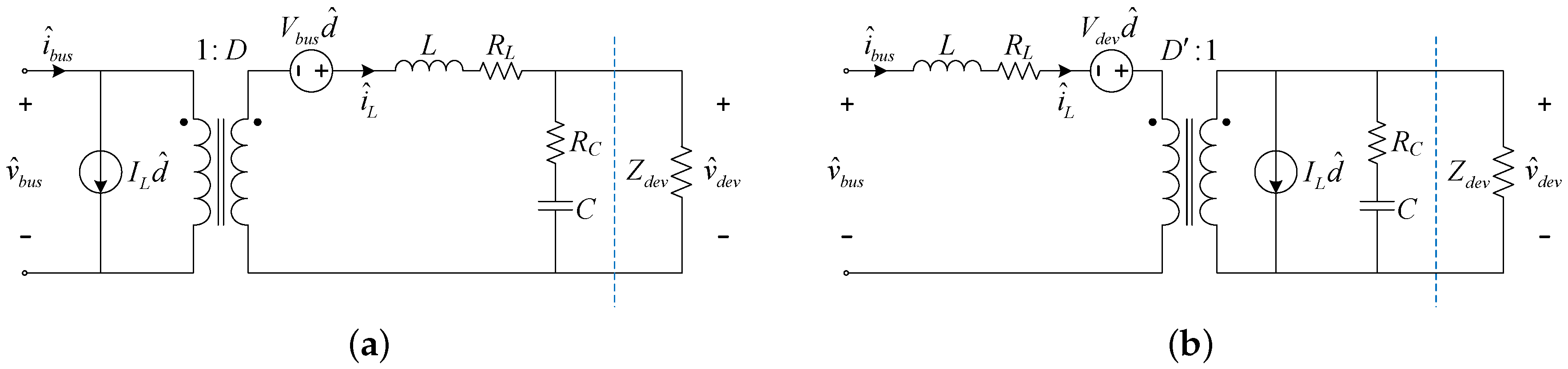
The small-signal averaged circuit model of a device-regulating converter is shown in
Figure 4, where
represents the input impedance of the device. The adopted bidirectional buck-boost converter is supposed to work in the buck mode when
and work in the boost mode when
. Only the continuous conduction mode (CCM) is considered here for simplification, since the device-regulating converters work in CCM for most cases. In the circuit model, the output impedance of bus-regulating converters is assumed to be zero, while the effect of the non-zero output impedance of bus-regulating converters on the dynamics of a device-regulating converter will be discussed in
Section 3.3.
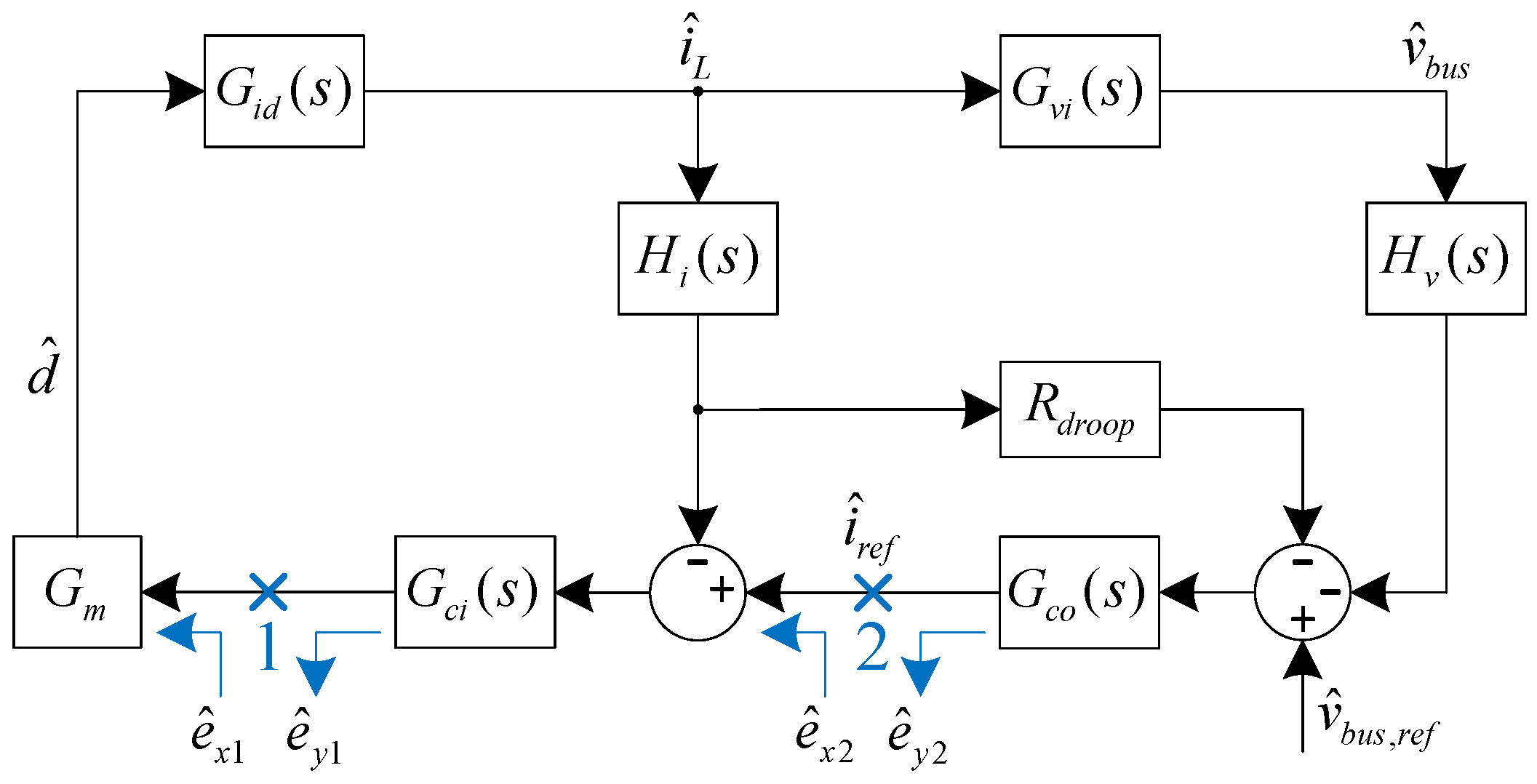
In the device-regulating converter, the average current mode control method is adopted to simplify the feedback control design, as well as to provide the required current limitation. The small-signal control block diagram of a device-regulating converter is shown in
Figure 5.
and
are the transfer functions from control variable
to inductor current
and device voltage
.
and
are the transfer functions from input voltage
to inductor current
and device voltage
.
and
are the current and the voltage sensing gains.
and
are the compensators of the inner current loop and outer voltage loop, respectively, and
is the gain of the pulse width modulator. The derivations of
,
,
and
for a device-regulating converter working in the buck mode or boost mode are expressed in
Table 2, where
,
and
. In the control design, the target crossover frequency of the inner current loop is
, while that of the outer voltage loop is
, where
is the converter switching frequency. The detailed design of the average current mode control for a device-regulating converter is a classic topic [
17,
18], so it will not be discussed here.
To derive the closed-loop input impedance of a device-regulating converter, the control loops depicted in
Figure 5 are expressed as Equation Set 1
The converter input current
can be expressed as the linear combination of
and
as below:
where
in the buck mode and
in the boost mode. Combining Equations 1 and 2, the closed-loop input impedance of a device-regulating converter is derived as:
Figure 6 shows a comparison between the derived closed-loop input impedance
and the incremental resistance
of a device-regulating converter when it operates at full power (500 W), where subscripts
and
represent that the converter works in the buck or boost mode. It can be seen that the incremental resistance
is a good approximation to
below the crossover frequency (
= 1 kHz) of the converter’s outer loop. Key parameters of the bidirectional buck-boost converter are shown in
Table 3. Other parameters used in this example are
= 24 V and
= 72 V. The incremental resistance
is derived based on
, which assumes no losses exist in a device-regulating converter, and it behaves as a constant power load/source.
is positive when the power is transferred from the DC bus to the device.
In a standalone DC microgrid,
n device-regulating converters operate on the bus simultaneously. Thus, the total closed-loop input impedance
of these converters can be expressed as the parallel combination of their respective input impedance
From Equation 4, it can be concluded that the input impedance
is determined by the net power
of the device-regulating converters. When
, which means the direction of the net power is towards the DC bus,
can be approximated as a positive resistance at frequencies below
. On the contrary, typical negative resistance appears when
.
3.2. Modeling and Control Design of the Bus-Regulating Converters
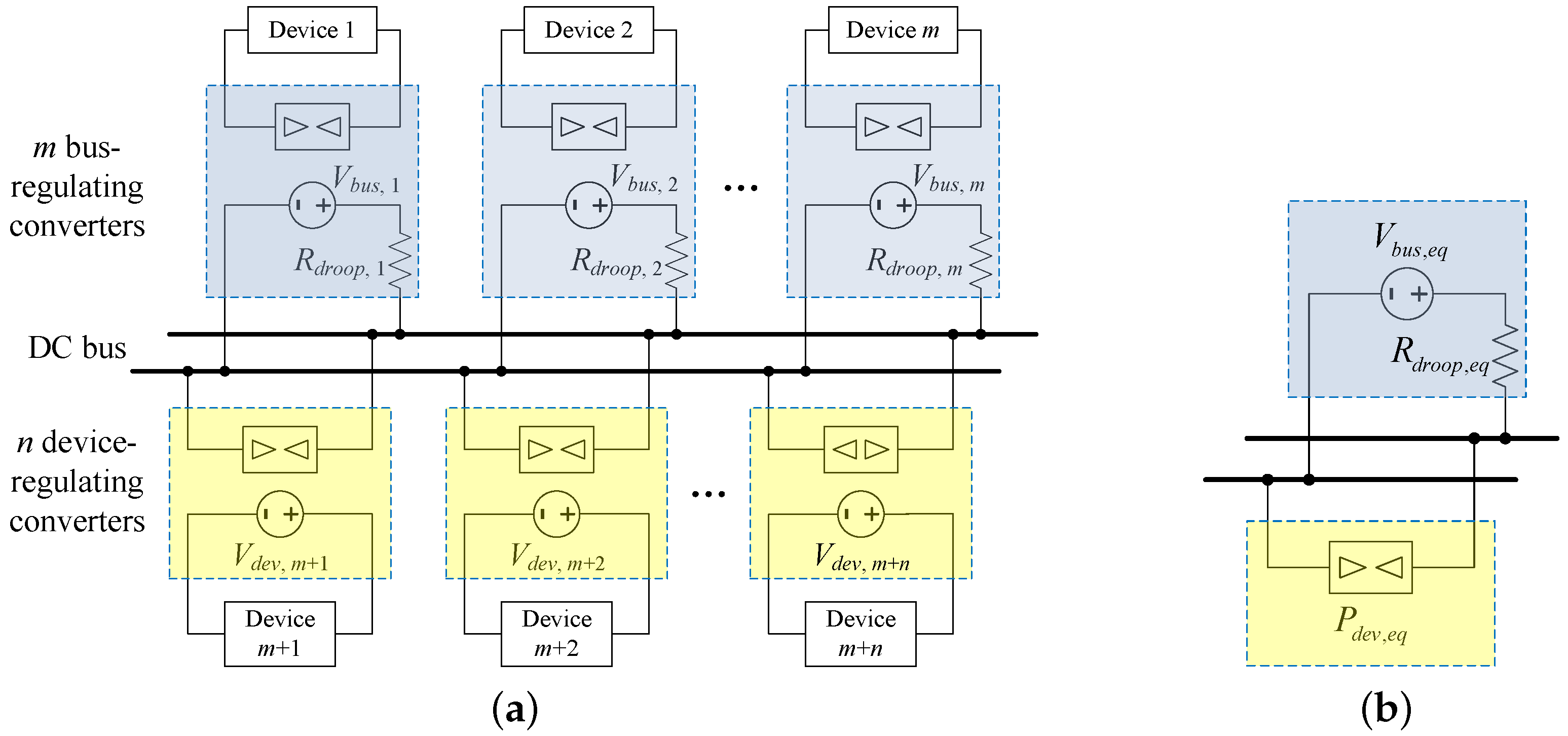
In a standalone DC microgrid, PV or battery converters work as the bus-regulating converters. Since a relatively low bus voltage of 48 V is chosen in this work, both PV and battery converters can easily be configured working in the buck mode.
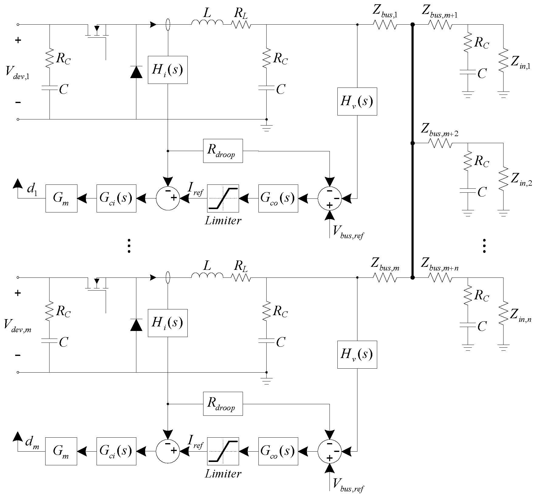
Figure 7 shows a circuit diagram where
m bus-regulating converters and
n device-regulating converters are interfaced to the DC bus.
represent the closed-loop input impedance of device-regulating converters.
represent the line impedance.
To develop the dynamic model of a bus-regulating converter,
,
and
can be combined into a single impedance
to represent their overall dynamics. When bus-regulating Converter 1 is analyzed,
can be expressed as:
Actually, a simplified expression of
can be derived as
if the bus impedance is neglected, where
is the total impedance of all bus capacitors.
The averaged small-signal circuit of a bus-regulating converter is depicted in
Figure 8;
is the equivalent small-signal resistance of the battery pack (
) or PV array (
). Both the CCM and the discontinuous conduction mode (DCM) are taken into account in the small-signal model, since the power processed by the bus-regulating converters varies with the net power
of device-regulating converters.
In this work, the small-signal model of the battery pack is represented as a voltage source
connected in series with its internal resistance
. The small-signal model of the PV array is represented as a current source
paralleled with a resistance
, in which
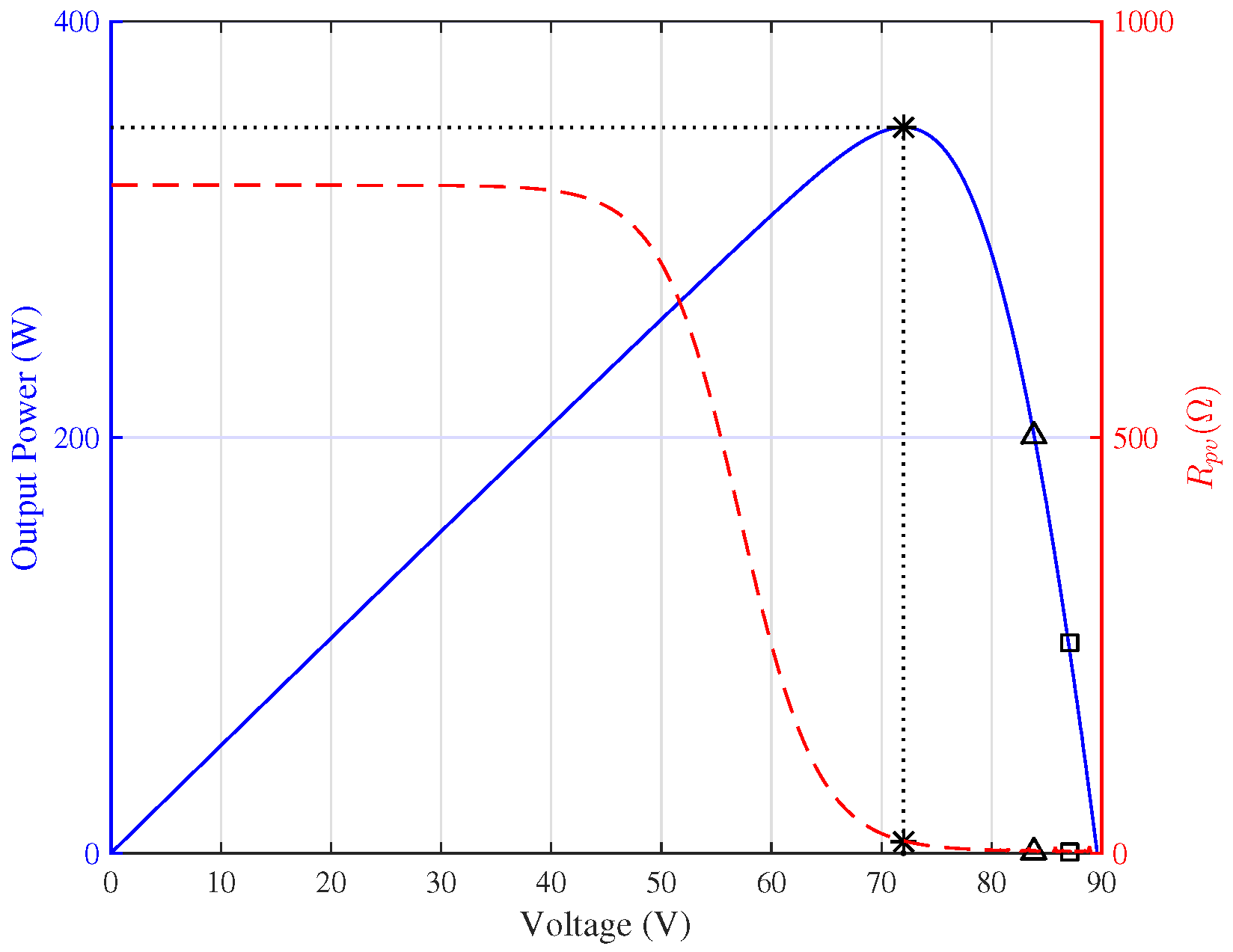
is obtained by the linearization of the nonlinear current-voltage curve of the PV array at its steady-state operating point. Values of
used in this work are shown in
Figure 9, which are obtained from a PV array model consisting of two series-connected Conergy P 175M PV modules.
When a bus-regulating converter works in CCM, the transfer functions of control to inductor current
and inductor current to bus voltage
are derived as follows:
where
. In DCM, the transfer functions of
and
are obtained as follows:
where
and
. The parameters used in DCM are shown in
Table 4, where
, and
M is the voltage conversion ratio [
19].
The control block diagram of the bus-regulating converters is shown in
Figure 10. To provide the required current limitation, average current mode control is also tried in the bus-regulating converters. The droop control method is adopted in the outer control loop for the purpose of current sharing.
The resulting expressions for the inner current-loop gain
and outer voltage-loop gain
are shown below:
where
and
are the compensators for the inner current loop and outer voltage loop, respectively. To achieve the desired crossover frequency and phase margin, different inner compensators
and
are designed according to the conduction mode of the inductor current. Whereas, the outer loop
is compensated using the same
. The detection of the conduction mode is implemented using the method in [
20].
It is a common practice to assume a resistive load in the control design of switching regulators. In this work, control loops
and
are designed based on
when the net power
of device-regulating converters is negative, since in this case, the total closed-loop input impedance
of device-regulating converters behaves as a positive resistance at low frequencies. Bode plots of
and
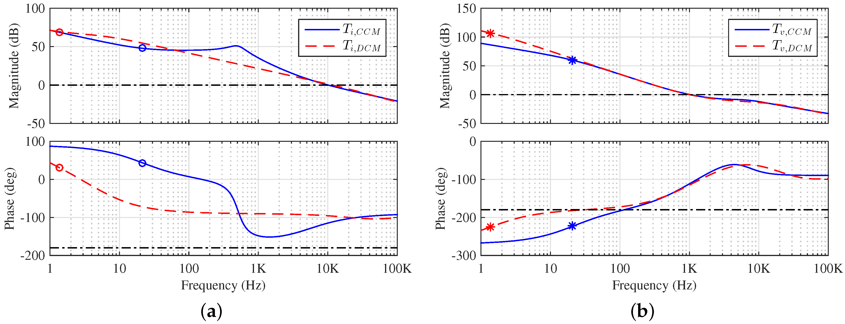
of a bus-regulating converter when it operates at −300 W (CCM) and −20 W (DCM) are shown in
Figure 11, where
,
and
are realized by PI compensators. Key parameters used in this example are
m = 2,
n = 6,
= 60 V,
= 20 mΩ,
= 10 mΩ and
= 25 mΩ. It can be seen that no right half-plane (RHP) zeroes or poles appear in the loop gains, so the stability and dynamic behavior of the converter could be analyzed using the Bode plots. As shown in the figure, the inner-loop crossover frequency
is 10 kHz, and the outer-loop crossover frequency
is 1 kHz, which all meet the design requirements,
and
. The phase margins of
and
are 65
and 88
, while the phase margins of
and
are 70
and 64
, respectively.
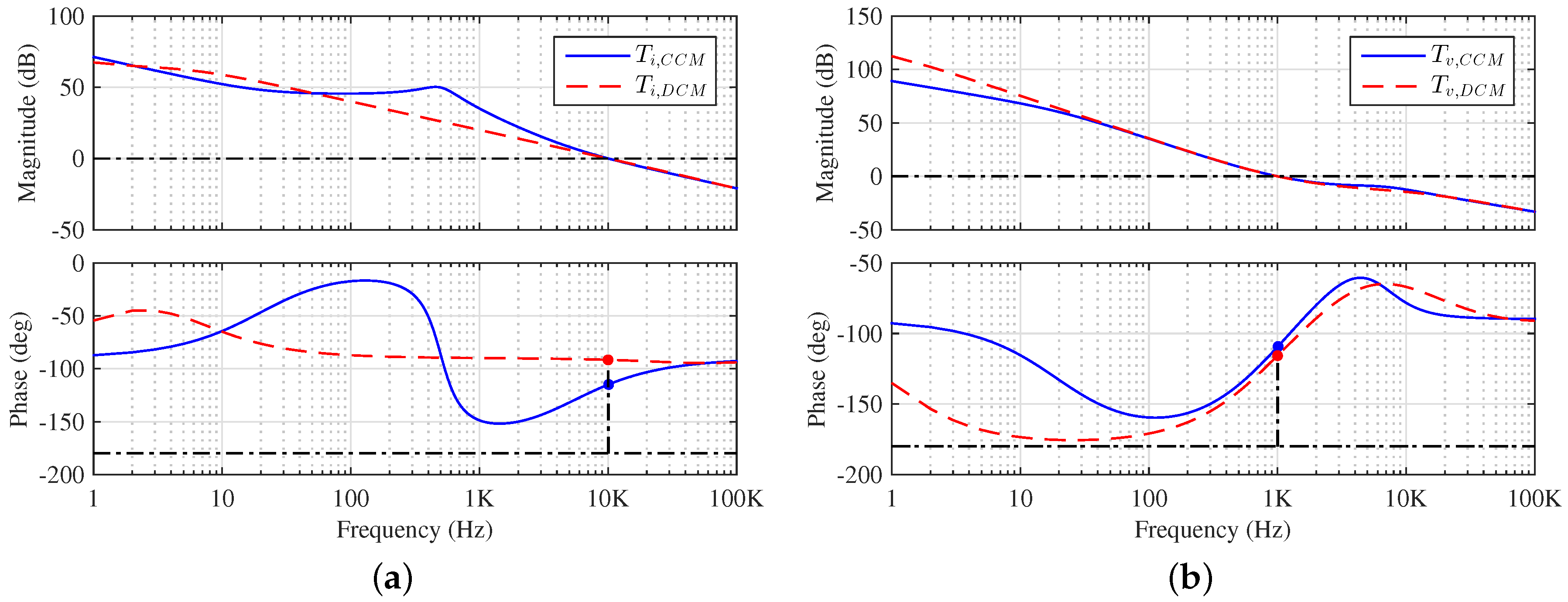
However, when
is positive,
behaves as a negative resistance at low frequencies, which results in one RHP zero in
and one RHP pole in
. The RHP zero and pole could be calculated numerically, and the effects of the RHP zeroes (circles) and poles (stars) can be observed in the Bode plots shown in
Figure 12. In this figure,
and
are calculated when the bus-regulating converter operates at 300 W (CCM) and 20 W (DCM), and the PI compensators designed above are still employed in the control loops.
So far, it has been demonstrated that loop gains
and
of a bus-regulating converter when
> 0 differ substantially from those when
< 0. When
> 0, Bode plots are no longer applicable to the stability analysis, since the RHP zero or pole appears. In order to analyze the stability of the bus-regulating converter, the Nyquist criterion has to be adopted. Actually, it is not difficult to find that the inner current loop
is no longer stable when
> 0 by using the Nyquist criterion. However, the stability of a multi-loop controlled converter is not determined by each loop alone, but by both loops working together. For the stability analysis of a bus-regulating converter, two loop gains
and
are measured, as shown in
Figure 13. Loop gain
is measured at Point “1”, while loop gain
is measured at Point “2”, where
and
are the small-signal perturbations injected for the measurement of the loop gain and
and
are their corresponding responses, respectively. These two loop gains have been verified regarding their importance in the stability analysis of a multi-loop controlled converter in [
21].
Loop gains
and
are expressed as follows:
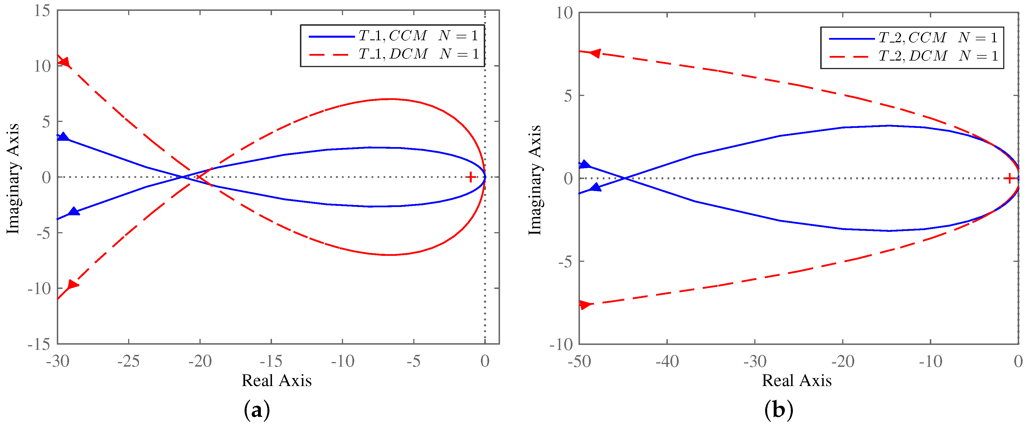
It is easy to find that actually
equals
; thus, one RHP pole exists in
. As for
, second-order poles appear at the original one due to the cascading of PI compensators. The statement of the Nyquist stability criterion for a continuous system is
, where
Z is the number of unstable closed-loop poles,
P is the number of unstable open-loop poles and
N is the number of counter-clockwise encirclements that the Nyquist plot of the loop gain makes around the
point. Nyquist plots of
and
are shown in
Figure 14. Both
and
encircle the
point counter-clockwise exactly once
. As one unstable pole exists in both
and
(
), the closed-loop system is proven to be stable (
) when
is positive.
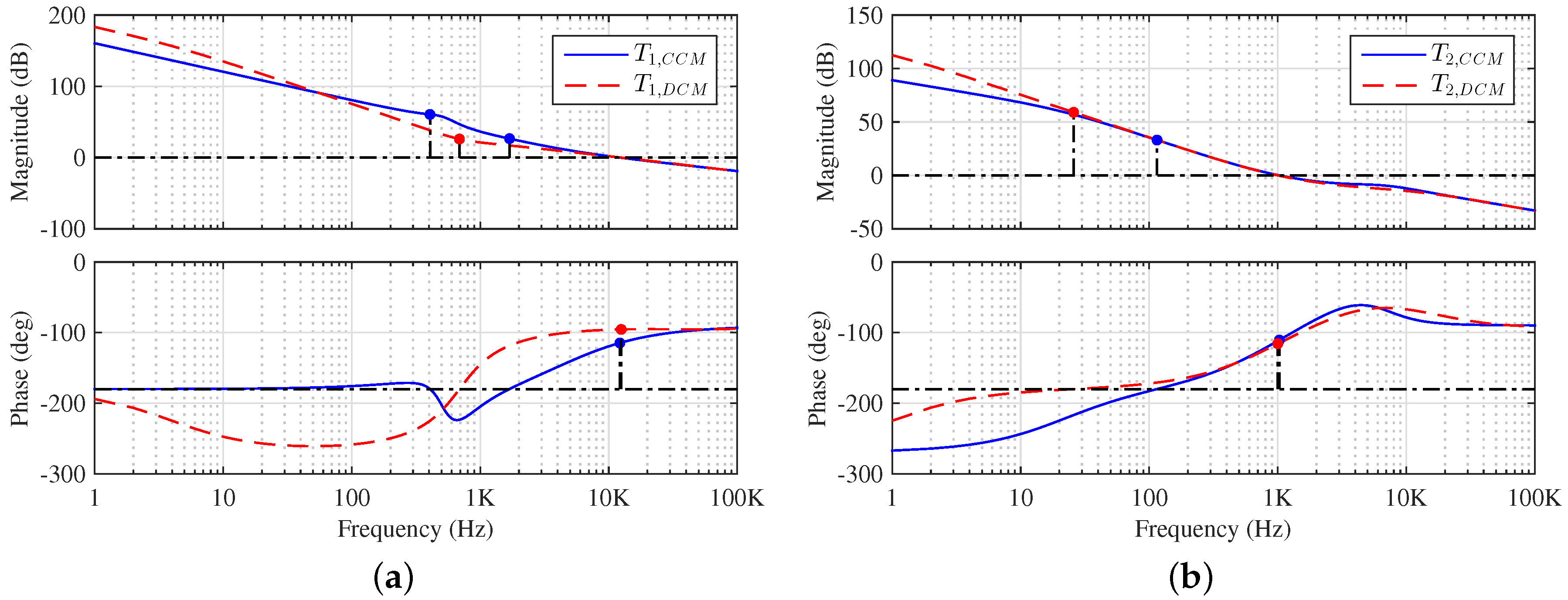
While the bus-regulating converter is proven to be stable when
, knowledge of the system relative stability is still necessary for us. As a result, gain and phase margins of
and
that are defined by the above Nyquist plots are translated into the Bode plots in
Figure 15. It can be seen that the control bandwidth of the inner loop is around 10 kHz, while that of the outer loop is 1 kHz, as desired. Fortunately, good system performance can be ensured by the gain and phase margins.
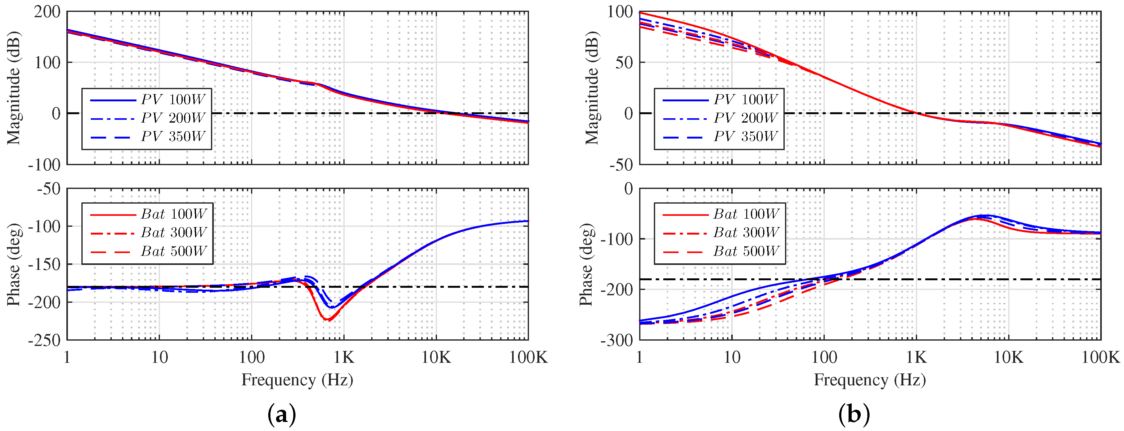
Furthermore, to regulate the DC bus voltage, battery and PV converters have to work over a wide range of operating conditions. To guarantee the performance of the bus-regulating converters, loop gains
and
are evaluated under several representative operating conditions. Three power levels (100 W, 200 W and 350 W) are picked out for the PV converters when the solar irradiance is 1000 W/m
and the temperature is 25
C. The PV output voltages
and the small-signal linearized resistances
corresponding to the three power levels are marked in squares (100 W), triangles (200 W) and stars (350 W) in
Figure 9. Three power levels (100 W, 300 W and 500 W) are also picked out for the battery converters. The battery voltage
and its internal series resistance
are assumed to be constant (
= 60 V,
= 20 mΩ) when different power is processed, since their variations are much less compared to the PV array.
Bode plots of
and
corresponding to the representative operating conditions are shown in
Figure 16. It should be appreciated that neither the gain nor the phase changes significantly over the power levels, device voltages or small-signal device resistances, especially at the crossover frequency. Similar results could also be obtained under other operating conditions, which allows one to conclude that the simple PI compensators designed for the bus-regulating control loops can be implemented under different operating conditions within a reasonable range.
3.3. Stability Analysis of the DC Microgrid
Based on the control loops designed in the above subsection (
Figure 13), the closed-loop output impedance
of a bus-regulating converter can be derived as follows:
Actually, the magnitude of
is verified to be quite close to
due to the adoption of the droop control method and average current mode control.
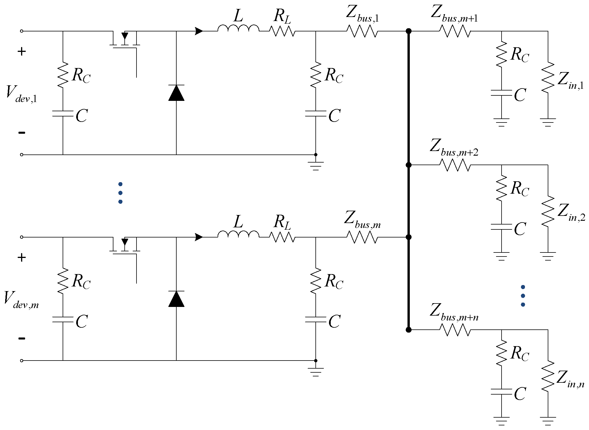
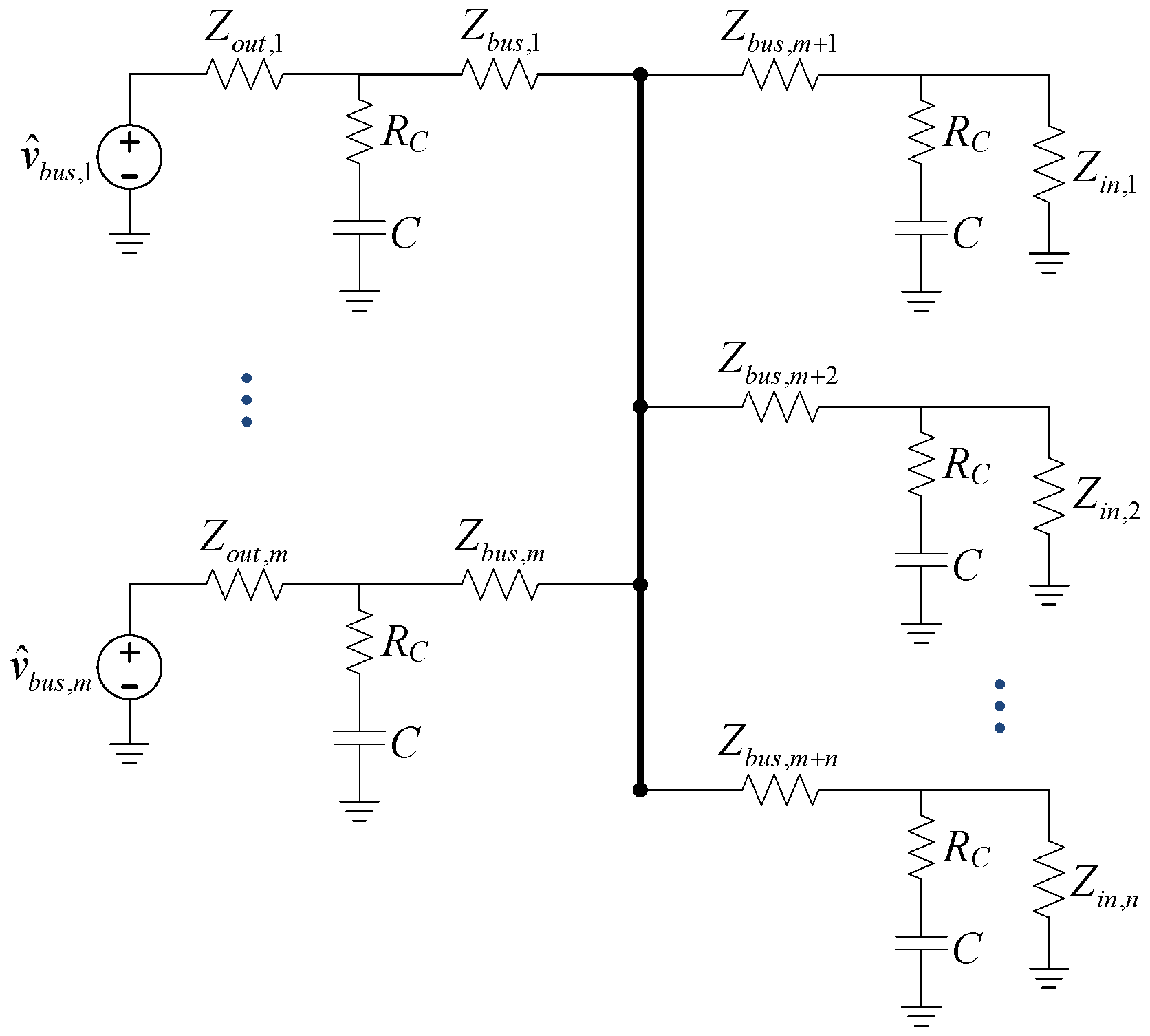
A small-signal equivalent circuit of the standalone DC microgrid can then be obtained in
Figure 17, where
m converters work in the bus-regulating mode and
n converters work in the device-regulating mode. Small-signal Thevenin sources (
,
) are used to model the closed-loop dynamics of the bus-regulating converters.
However, when the closed-loop input impedance
is derived in
Subsection 3.1, it is assumed that the output impedance
of bus-regulating converters is zero. Therefore, it needs to be determined that whether the transfer functions (
,
) that were used to derive
in
Subsection 3.1 are modified by the none-zero output impedance
. Middlebrook’s extra element theorem (EET) [
5,
19] is employed here to determine how the addition of
alters these transfer functions. Take
as an example. The modified transfer function can be expressed as follows:
where
is the transfer function
derived in
Section 3.1 and
is the combination of
,
and
. When device-regulating Converter 1 is analyzed,
can be expressed as below:
Additionally, a simplified expression of
is derived as below if the bus impedance is neglected:
The definition and derivation of the impedance
and
for a device-regulating converter are described in
Table 5.
From Equation 16, it can be easily obtained that when the inequalities of
and
are satisfied,
, which means the control loops of the device-regulating converter are not interfered with obviously. Therefore, the comparison between
and
,
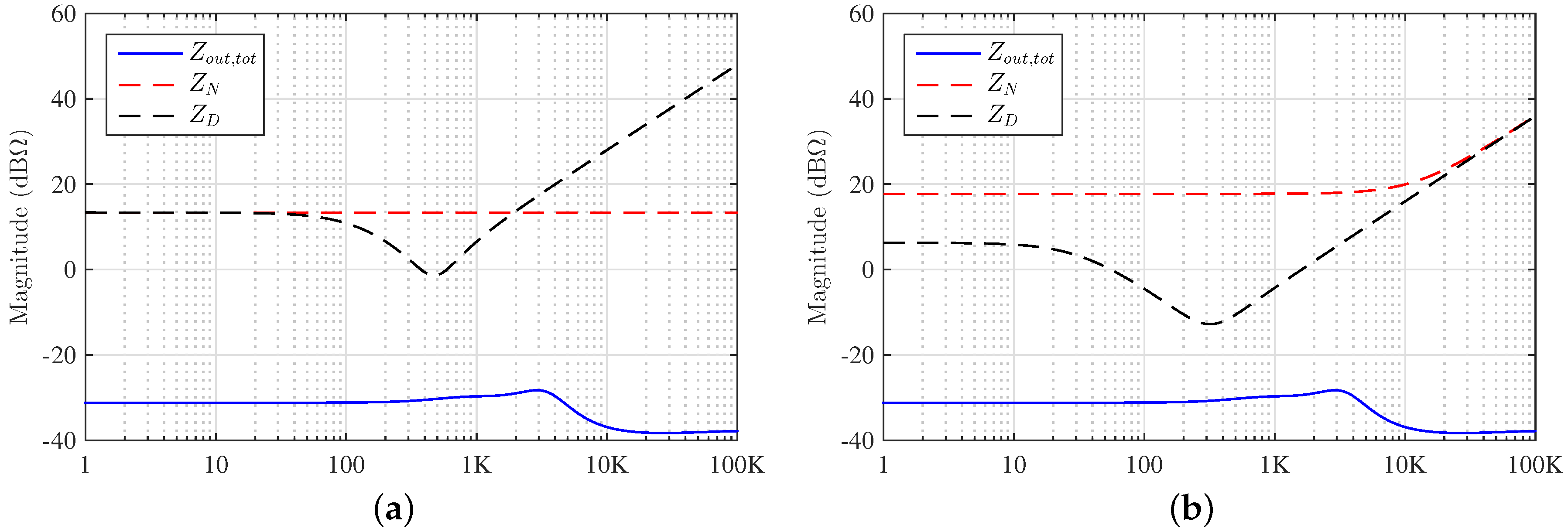
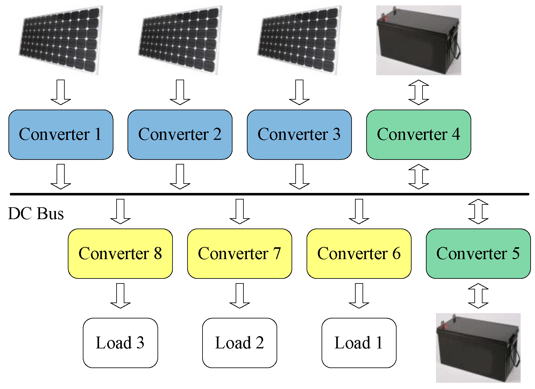
needs to be implemented. A standalone DC microgrid, which consists of eight distributed power modules, is taken as an example, where two battery converters work in the bus-regulating mode; three PV converters and three load converters work in the device-regulating mode. The power processed by each converter is listed as follows:
= 300 W,
= 300 W and
= 500 W. The comparison result is shown in
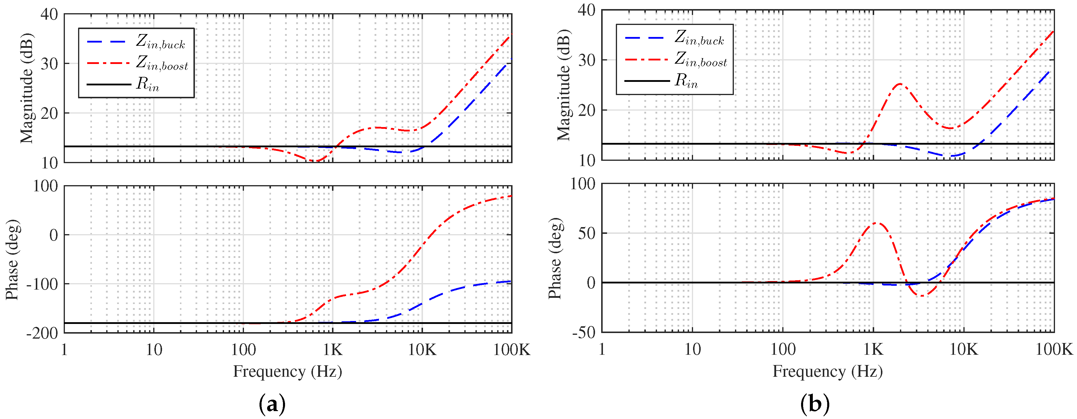
Figure 18, where both the load converter (buck mode) and the PV converter (boost mode) are analyzed. It can be concluded that the control loops of the device-regulating converter are not affected significantly by the non-zero output impedance of the bus-regulating converters, since a wide separation can be observed between
and
,
. Therefore, the closed-loop input impedance
derived in
Subsection 3.1 is proven to be a good approximation to the value when
is taken into account.
Since it has already been verified in
Section 3.2 that the stability and performance of the designed bus-regulating control loops are not affected considerably by the input impedance of device-regulating converters, a low degree of interaction among the distributed converters can be predicted in the designed standalone DC microgrid, and the system is stable.


