Article

A Nature-Inspired Optimization-Based Optimum Fuzzy Logic Photovoltaic Inverter Controller Utilizing an eZdsp F28335 Board

by
Ammar Hussein Mutlag
1,2,*,
Azah Mohamed
1 and
Hussain Shareef
3
1
Department of Electrical, Electronic and Systems Engineering, Faculty of Engineering and Built Environment, Universiti Kebangsaan Malaysia, 43600 Bangi, Selangor, Malaysia
2
College of Electrical and Electronic Engineering Techniques, Middle Technical University, 10022 Baghdad, Iraq
3
Department of Electrical Engineering, United Arab Emirates University, 15551 Al-Ain, UAE
*
Author to whom correspondence should be addressed.
Energies 2016, 9(3), 120; https://doi.org/10.3390/en9030120
Submission received: 9 December 2015 / Revised: 19 January 2016 / Accepted: 5 February 2016 / Published: 23 February 2016

Abstract

:
Photovoltaic (PV) inverters essentially convert DC quantities, such as voltage and current, to AC quantities whose magnitude and frequency are controlled to obtain the desired output. Thus, the performance of an inverter depends on its controller. Therefore, an optimum fuzzy logic controller (FLC) design technique for PV inverters using a lightning search algorithm (LSA) is presented in this study. In a conventional FLC, the procedure for obtaining membership functions (MFs) is usually implemented using trial and error, which does not lead to satisfactory solutions in many cases. Therefore, this study presents a technique for obtaining MFs that avoids the exhaustive traditional trial-and-error procedure. This technique is implemented during the inverter design phase by generating adaptive MFs based on the evaluation results of the objective function formulated with LSA. The mean squared error (MSE) of the inverter output voltage is used as an objective function in this study. LSA optimizes the MFs such that the inverter provides the lowest MSE for the output voltage, and the performance of the PV inverter output is improved in terms of amplitude and frequency. First, the design procedure and accuracy of the optimum FLC are illustrated and investigated through simulations conducted in a MATLAB environment. The LSA-based FLC (LSA-FL) are compared with differential search algorithm (DSA)-based FLC (DSA-FL) and particle swarm optimization (PSO)-based FLC (PSO-FL). Finally, the robustness of the LSA-FL is further investigated with a hardware that is operated via an eZdsp F28335 control board. Simulation and experimental results show that the proposed controller can successfully obtain the desired output when different loads are connected to the system. The inverter also has a reasonably low steady-state error and fast response to reference variation.

1. Introduction

Nowadays, renewable energy (RE) has become the main impetus of the energy sector, primarily because it is environment friendly, clean, and a secure energy source [1]. Among REs, photovoltaic (PV) power generation is one of the most promising technologies that can be utilized in industrial power systems and rural electrification [2]. Given that PV generators can only supply DC power, an inverter is required to connect the load to PV generators [3]. The main feature of a good power inverter is its capability to provide clean, high-quality power and constant amplitude sinusoidal voltage and frequency, regardless of the load type to which it is connected. Furthermore, a power inverter must also have the capability to recover quickly from transients caused by external disturbances without causing power quality problems. In the context of a stand-alone PV generator, the output voltage and current waveforms should be controlled based on the reference values. Therefore, an efficient PV inverter controller is required [4]. However, the extensive use of PV generators raises many challenges, such as harmonic pollutions, low efficiency of energy conversion, fluctuation of output power, and reliability of power electronic converters [5].
Numerous PV inverter controllers have been suggested by many researchers to solve these problems. A proportional integral (PI) controller is a widely accepted technique in inverter controls. Selvaraj et al. [6] implemented a digital PI current control algorithm in a PV inverter through a eZdsp F2812 to maintain the current fed into the utility grid network to be sinusoidal. However, this PI controller requires trapezoidal sum approximation to transform the integral term into a discrete-time domain. Similarly, Sanchis et al. [7] proposed a traditional PI controller to control a DC-to-AC boost converter. However, their controller requires the differential equations of the system to obtain good performance. In a related work, PI controllers were implemented for a three-phase inverter utilizing dSPACE DS1104 control hardware [8]. However, the method of tuning the gains of PI controllers has not been elaborated. In recent years, researchers have focused on the utilization of optimization techniques in PI controller tuning to achieve improved performance. An optimal DC bus voltage regulation strategy with PI controllers for a grid-connected PV generator was suggested in [9]. In this research, PI control parameters were optimized through simplex optimization technique. Various other optimization methods, such as particle swarm optimization (PSO), have also been used in PI controller parameter tuning for different applications [10,11,12,13]. The performance of a PI controller is limited to small load disturbances. Its design is based on an accurate mathematical model of the real system under consideration, and it needs appropriate setting of its parameters.
Artificial intelligence-based controllers have been used in inverters with high efficiency and great dynamics. Various methods, including artificial neural network (ANN), fuzzy logic, and adaptive neuro fuzzy inference system (ANFIS)-based controllers, were reported in the literature. ANN-based maximum power point tracking controller in a PV inverter power conditioning unit was proposed in [14]. In this work, the ANN module was used to estimate the voltages and currents corresponding to a maximum power delivered by PV panels. The module was then utilized to obtain the desirable converter duty cycle. Nonetheless, this proposed controller requires a large amount of training data before it can be trained and implemented in the controller. Fuzzy logic controllers (FLCs) have become increasingly popular in designing inverter controls because of their simplicity and adaptability to complex systems without a mathematical model [15]. Some good examples of FLCs for inverter control can be found in [16,17]. In these studies, two individual FLCs were used to control both the DC–DC and DC–AC converter in a fuel cell grid-connected inverter and stand-alone PV inverter, respectively. The authors claimed that acceptable results can be achieved with seven membership functions (MFs) and that the proposed technique can be implemented easily. In [18], the interval type-II fuzzy rule-based static synchronous compensator (STATCOM) for voltage regulation in a power system has been investigated. The interval type-II fuzzy rule base utilizes the output of the PID controller to tune the signal applied to the STATCOM to mitigate bus voltage variation caused by large changes in load and intermittent generation of PV arrays. Nonetheless, the performance of FLC depends on the rule base, number of rules, and MFs. These variables are determined based a trial-and-error procedure which is time consuming [19]. Therefore, various techniques, such as neuro-fuzzy model and other optimization techniques were proposed in the literature to overcome the limitations of the FLC design. In [20], Collotta et al. developed a neuro-fuzzy model for dynamic and automatic regulation of indoor temperature. The ANN is applied to forecast indoor temperatures that are used to feed a FLC unit to manage the on/off switching of the ventilating and air-conditioning system and the regulation of the inlet air speed. However, neuro-fuzzy model requires extensive training data similar to ANN controllers and that training data are difficult to obtain in many cases. In [21], a particle swarm optimization (PSO) algorithm was applied to optimize a FLC for maximum power point tracking of a PV system. The selection of a proper optimization technique is important because PSO is prone to premature convergence. To date, such adaptive MF tuning method has not been applied in a FLC for PV inverter control.
In the proposed research, the LSA is developed to enhance the performance of the fuzzy logic controller for the three-phase PV inverter. The proposed approach aims to solve the problem of trial-and-error procedure in obtaining MFs used in the conventional FLC. LSA is a novel nature-inspired technique formulated to solve both single-modal and multimodal optimization problems. This algorithm is particularly recommended to solve multimodal problems, such as for tuning the MFs of the FLC [22]. Therefore, the utilization of the LSA improves the performance of the FLC for PV inverters. LSA optimizes the MFs of the FLC based three-phase inverter by minimizing the objective function which is the mean squared error (MSE) of the output voltage. The system is first modeled in the MATLAB environment and then implemented in the eZdsp F28335 control board (Spectrum Digital Inc, Stafford, TX, USA) to validate the performance of the proposed controller by considering perturbation such as change in DC input voltage and load.

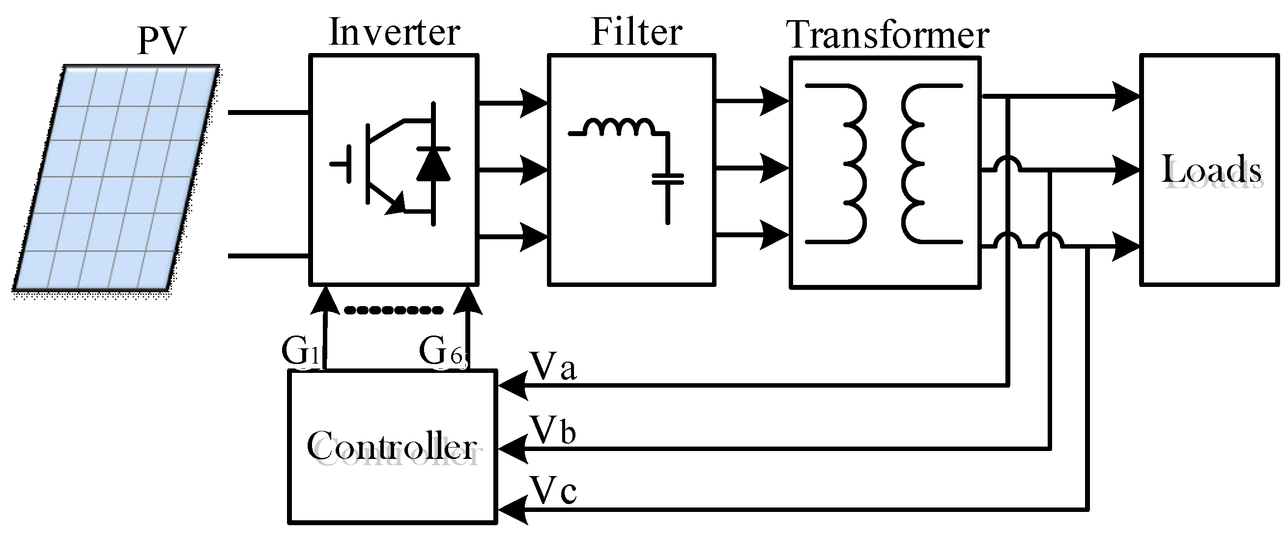
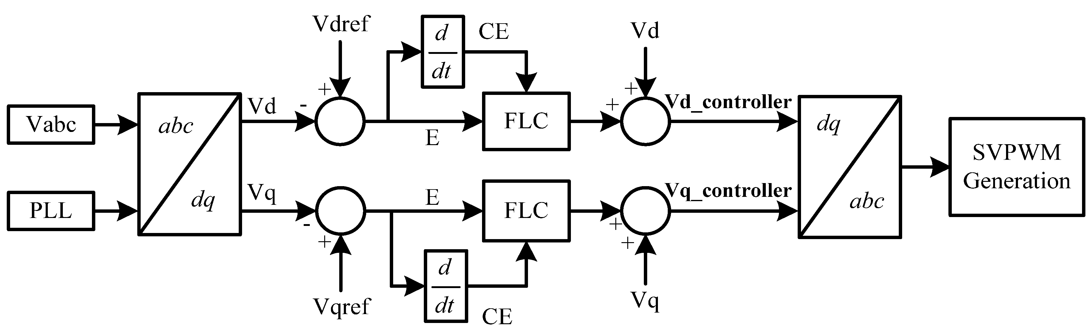
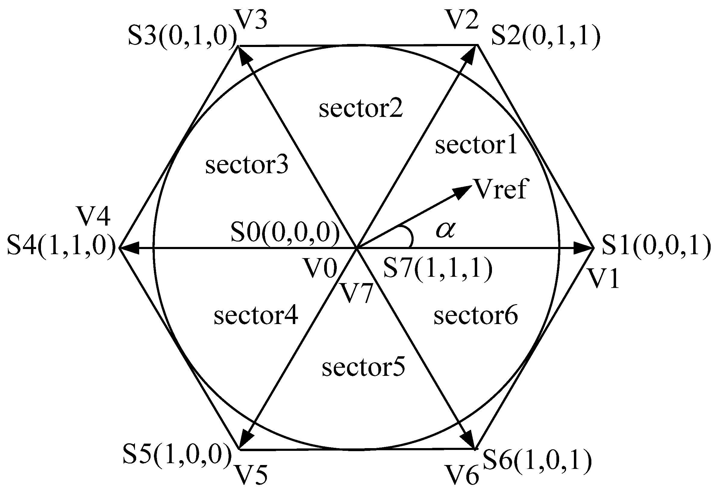
2. Inverter Control Algorithm

Inverter control aims to regulate the AC output voltage at a desired magnitude and frequency with low harmonic distortion. This regulation is performed by the controller by implementing a proper control algorithm to maintain the voltage at a set reference. The structure of the standalone PV inverter used in this study is shown in Figure 1 to illustrate the main control loops for achieving the aforementioned control objective. This inverter consists of a DC input from the PV source, DC–AC inverter, transformer, and load. This type of inverter with a DC input source is known as a VSI.
To apply the control algorithm in the inverter system, the three-phase output voltages in the synchronous reference frame must be sensed at the load terminals through the appropriate voltage sensors. The three-phase output voltages of the load terminal (Va, Vb, and Vc) can be represented as:
V a = V   sin   ω t
V b = V   sin   ( ω t 2 3 π )
V c = V   sin   ( ω t + 2 3 π )
where V is the voltage magnitude, and ω is the output frequency. These voltages (Va, Vb, and Vc) are then scaled and transformed into a d–q reference frame to simplify the calculations for controlling the three-phase inverter [23,24]. The two DC quantities, namely, Vd and Vq, can be obtained by applying Park’s transformation, as shown in Equation (4). This transformation employs a 50 Hz synchronization signal from a phase-locked loop block:
[ V d V q V o ] = 2 3 [ cos ( ω t ) cos ( ω t 2 π 3 ) cos ( ω t + 2 π 3 ) sin ( ω t ) sin ( ω t 2 π 3 ) sin ( ω t + 2 π 3 ) 1 2 1 2 1 2 ] × ( V a V b V c )
The error E between the measured voltages Vd and Vq and reference voltages Vdref and Vqref per unit can then be computed. Similarly, the change in error CE can be determined by taking the derivative of E. These signals (i.e., E and CE) are then sent to the controller at each sampling time Ts to compute the missing components in Vd and Vq and to generate the new Vd and Vq signals. The new Vd and Vq are again converted into the synchronous reference frame voltages Va, Vb, and Vc through the following equation:
[ V a V b V c ] = 2 3 [ cos ( ω t ) sin ( ω t ) 1 cos ( ω t 2 π 3 ) sin ( ω t 2 π 3 ) 1 cos ( ω t + 2 π 3 ) sin ( ω t + 2 π 3 ) 1 ] × ( V d V q V o )
These voltages can be applied in generating the pulse width modulation (PWM) to drive the insulated-gate bipolar transistor IGBT switches in the inverter block in Figure 1. As a result of inverter switching, a series of pulsating DC input voltage Vdc appears at the output terminals of the inverter. Given that the output voltages of the inverter are pulsating DC voltages, an appropriate low-pass filter must be used (Figure 1) before importing PV-generated electrical energy to the load. The design procedure of the filter circuits can be found in [25].

3. Inverter Control Using FLC Strategy
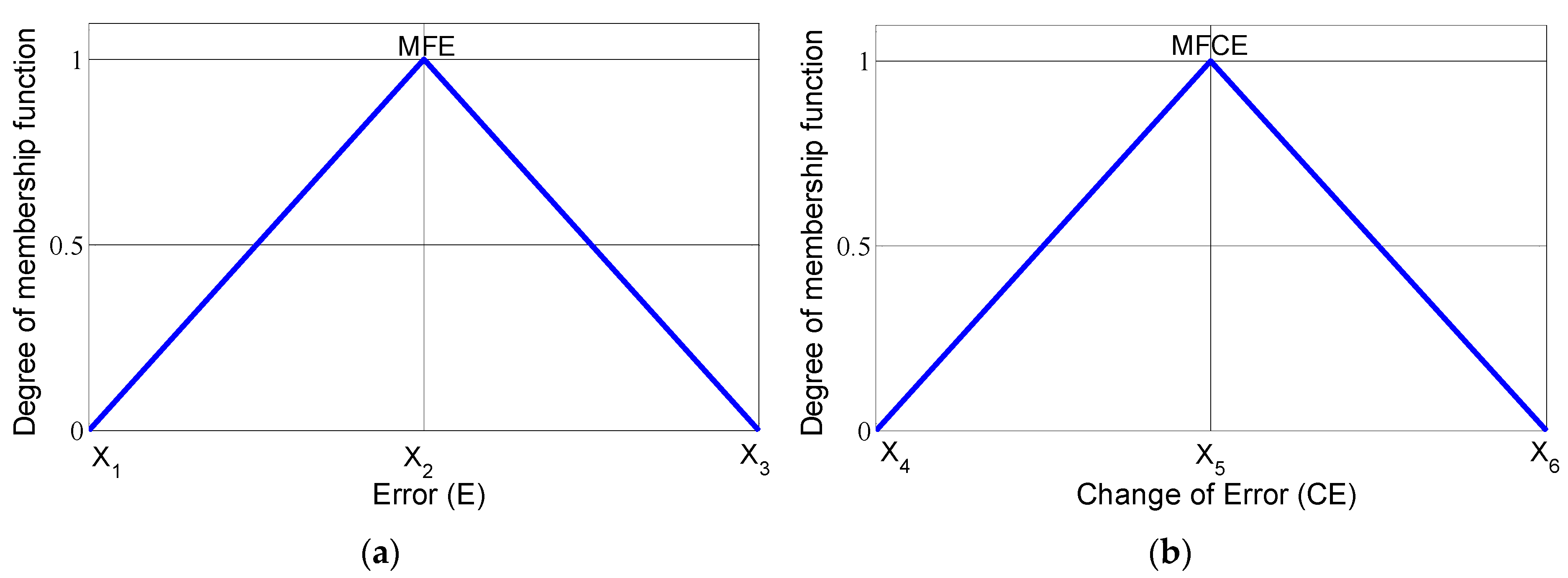
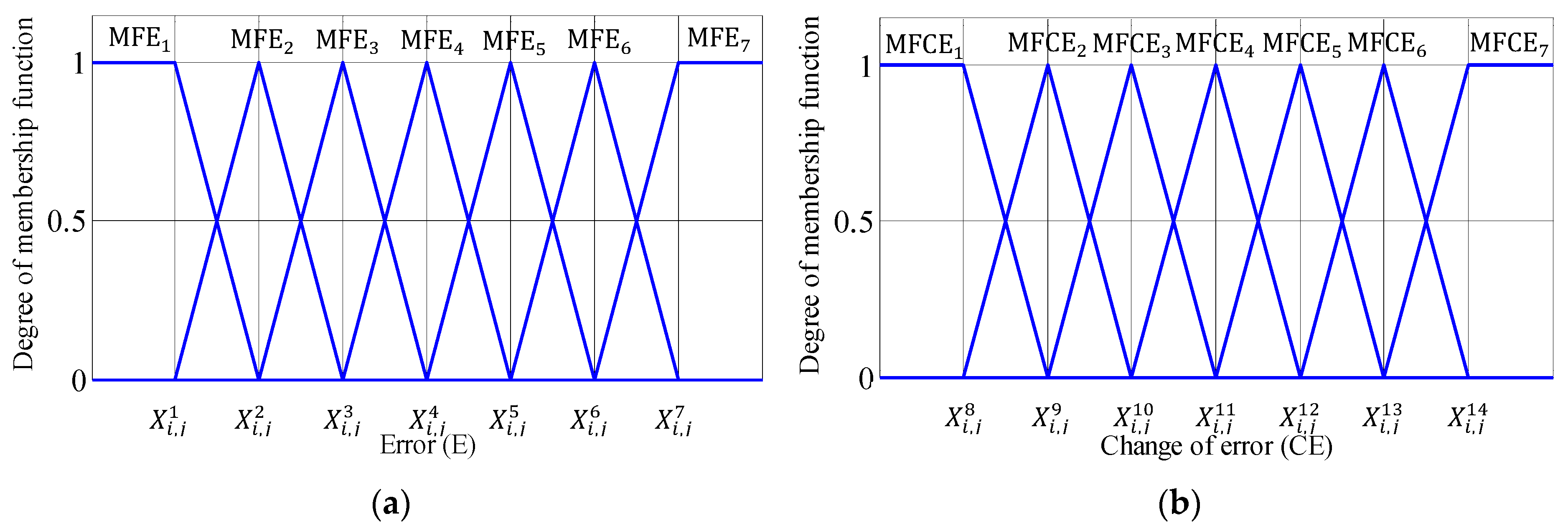
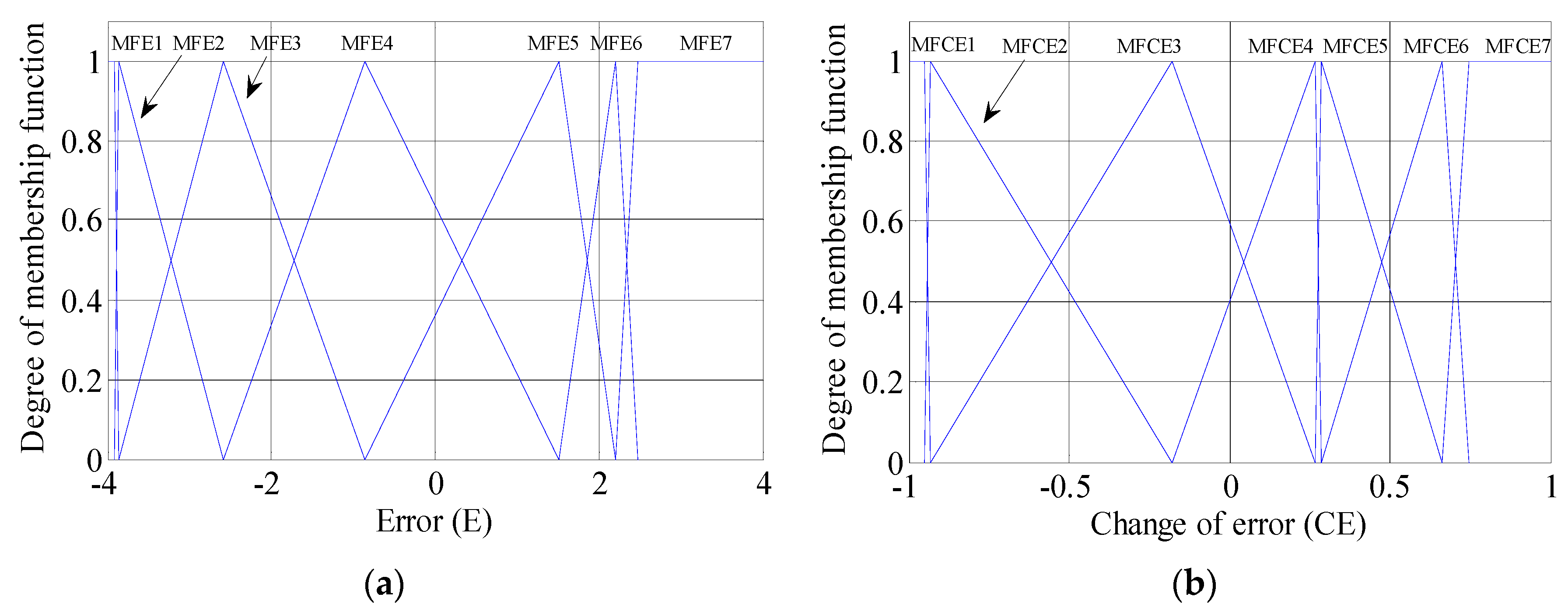
In consideration of the nonlinearity of the power conversion process in PV inverters, fuzzy logic is a convenient method to adopt in a PV inverter control system. An FLC represents the human expert decision in the problem solving mechanism. The main advantages of FLC are:
  • FLC can be used in many applications especially for control and modeling of non-linear systems [19].
  • FLC is less dependent on a mathematical model and system parameters [26].
  • FLC is based on linguistic rules with an if-then general structure, which is the basis of human logic [27].
Figure 2 shows the inverter control concept with FLC as a control strategy.
The first step in FLC is to select the number of inputs and outputs. In this work, where FLC serves as a PV inverter controller, E and CE are used as inputs, whereas the missing component of Vd or Vq defined as O is used as the output of the FLC. The two inputs for the FLC depicted in Figure 2, namely, E and CE, at the tth sampling step that corresponds to Vd can be described as follows:
E ( t ) = V d r e f V d ( t )
C E ( t ) = E ( t ) E ( t 1 )
The output O for this case can be obtained at the last stage of the FLC design, which is explained in the next section. The FLC design must pass through the following steps, namely, fuzzification, inference engine design, and defuzzification [28,29].

3.1. Fuzzification

After the inputs and outputs are defined, the next stage involves the fuzzification of inputs. This step represents the inputs with suitable linguistic value by decomposing every input into a set and by defining a unique MF label, such as “big” or “small”. Thus, the number of MFs used in the FLC depends on the linguistic label. The MFs of E and CE for the FLC can be defined as trapezoidal and triangular MFs. This process translates the crisp values of “E” and “CE” as the fuzzy set “e” and “ce”, respectively, through the MF degrees µe(E) and µce(CE), which range from 0 to 1, as shown in Figure 3 for triangular MFs. In Figure 3a, the MF of error (MFE) is defined by three elements, namely, X1, X2, and X3, whereas the MF of change of error (MFCE) in Figure 3b is defined by another three elements represented by X4, X5, and X6.
After defining the MFs, µe(E) and µce(CE) can be calculated with a basic straight line equation that consists of two points. For example, µe(E) and µce(CE) for the MFs in Figure 3 can be expressed as follows:
µ e ( E ) = { E X 1 X 2 X 1 X 1 E < X 2 1 + X 2 E X 3 X 2 X 2 E < X 3
µ c e ( C E ) = { C E X 4 X 5 X 4 X 4 C E < X 5 1 + X 5 C E X 6 X 5 X 5 C E < X 6
In a standard FLC design, the selection of the number of MFs and the boundary values of each MF must be adjusted by the designer by using the trial-and-error method until the FLC provides a satisfactory result. However, this process is time consuming and laborious. After the inputs are fuzzified, the fuzzy inputs are subjected to an inference engine to generate a fuzzy output.

3.2. Inference Engine Design

This stage represents the decision making process based on the information from a knowledge base, which contains linguistic labels and control rules. Two types of inference systems mainly exist, namely, Mamdani type and Sugeno type. The Mamdani-type inference system is adopted in this study because of its simple implementation steps. The rules with two inputs for the Mamdani type can be written as follows:
R: IF E is “label” AND CE is “label,” THEN u is “label.”
The quantity of rules depends on the number of inputs and MFs used in the FLC [28,29]. An FLC with a large rule base demands great computational effort in terms of memory and computation time.

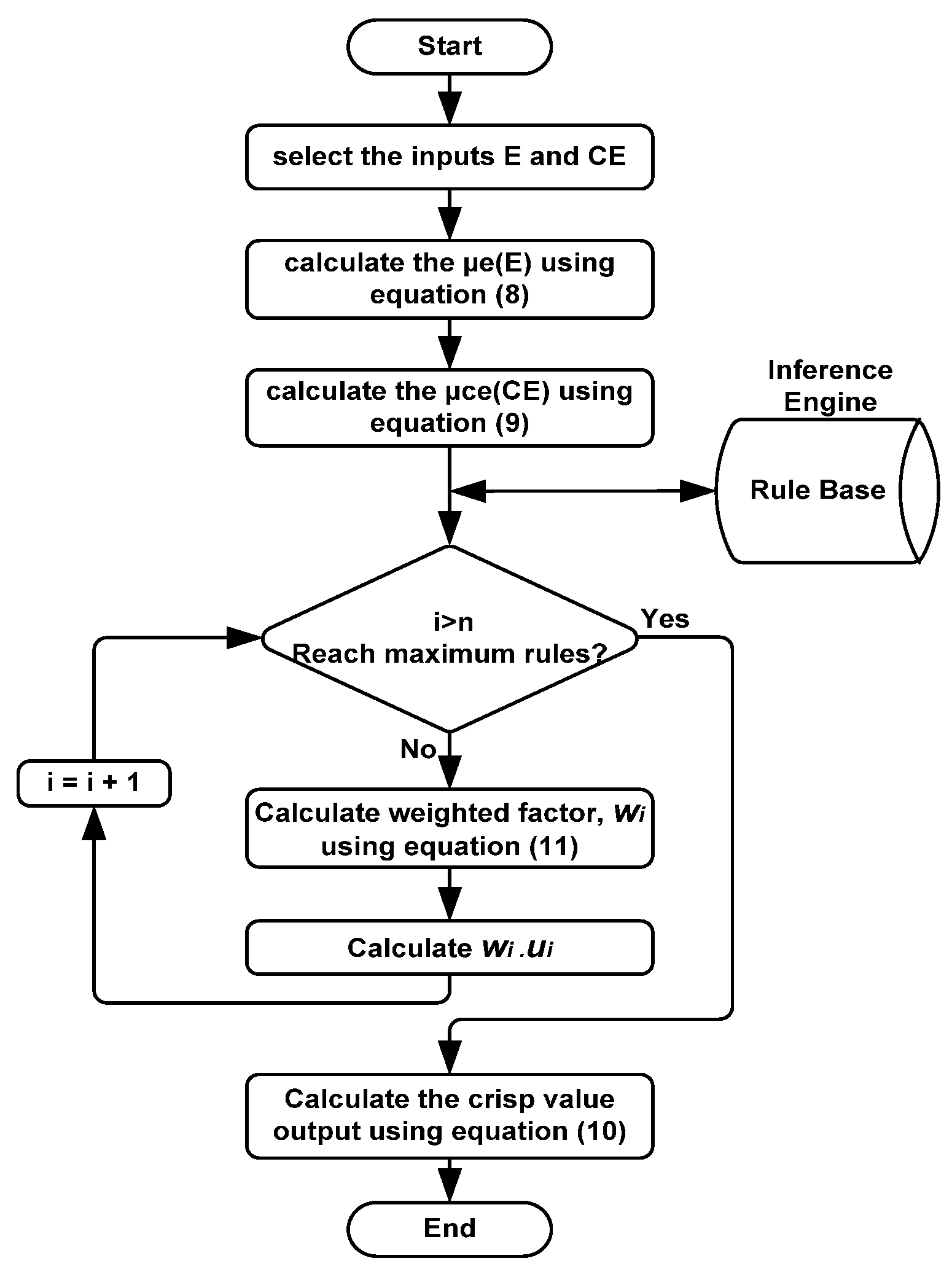
3.3. Defuzzification

The final step in the FLC is the selection of the defuzzification method. This process generates a fuzzy control action as a crisp value. Several methods can be used to generate the crisp value. The most common methods include the center of area (COA) and the mean of maximum (MOM) methods. The widely used COA method generates the center of gravity of the MFs. In this study, the COA method given in Equation (10) is used to generate the crisp value because it is more accurate than MOM method [28]:
C O A = i = 1 n w i · u i i = 1 n w i
where n is the number of rules, and wi is the weighted factor that can be calculated with Mamdani-MIN between µe(E) and µce(CE), as expressed by:
w i = M I N   [ µ e ( E ) , µ c e ( C E ) ]
The implementation steps of the standard FLC are illustrated in Figure 4.

4. Proposed Optimum FLC Design Procedure

As noted in the standard FLC design procedure, the main drawback of FLC design is the time-consuming trial-and-error process used to adjust the boundary values of MFs in the fuzzification process. Improper selection of MF boundaries may lead to the poor performance of the overall system. Therefore, this work presents a methodology to optimize MFs through a heuristic optimization algorithm. A heuristic optimization algorithm is used to solve complex and intricate problems that are otherwise difficult to solve with classical methods. It is a population-based method designed to solve a problem quickly or to determine an approximate solution when classic methods fail to determine a solution particularly with multimodal optimization problems. LSA has been developed as a heuristic optimization tool to adjust the boundary values of MFs adaptively because of its suitability for multimodal problems, such as the FLC design for PV inverter control.

4.1. Overview of LSA

LSA is a nature-inspired metaheuristic optimization algorithm [22]. LSA is based on the natural phenomenon of lightning. The probabilistic nature and tortuous characteristics of lightning discharges originate from a thunderstorm. The proposed optimization algorithm is generalized from the mechanism of step leader propagation. It considers the involvement of fast particles known as projectiles in the formation of the binary tree structure of a step leader. Three projectile types are used to represent the transition projectiles that create the first step leader population N, the space projectiles that attempt to become the leader, and the lead projectile that represents the best positioned projectile that originated among N number of step leaders. The details of the LSA, including its basic concepts and algorithms, can be found in [22].

4.2. Optimal FLC Problem Formulation

The three basic components that are considered in any optimization method are input vectors, objective function formulation, and constraints. Each component is developed and clarified to obtain the optimal MFs. The optimization technique searches the optimal solution as formulated in the objective function through manipulation of the input vector subject to the constraints in each generation of the iterative process.

4.2.1. Input Vector

As the first step in FLC design, the number of MFs must be defined to provide the solution from the optimization technique. Depending on the number of MFs, the input vector Z can be described by:
Z i , j = [ X i , j 1   X i , j 2 X i , j n ]
where Zi,j represents the jth solution in the population during the ith iteration, X i , j k is the kth element of Zi,j, and n is the total number of parameters. For example, the input vector Zi,j should contain six parameters indicating the boundaries of MFs that should be optimized to represent the MFs in Figure 3.

4.2.2. Objective Function

An objective function is required to determine and evaluate the performance of Zi,j for the MFs. Thus, the objective function to determine the optimal values is formulated in such a way that Zi,j generates the best fuzzy control action as a crisp value according to Equation (10) described in the defuzzification process. In the FLC design for the PV inverter control, E and CE at the tth sampling step that corresponds to Vd (which is the transformed inverter output voltage) indicate the goodness of the crisp value of the fuzzy control action. Therefore, the MSE (13) obtained from the reference values Vdref and the measured values Vd are used as the objective function:
M S E = i = 1 ( V d r e f V d ) 2
where Vdref is the reference value that is equal to (1 p.u.), Vd is the measured value, and is the number of the samples used to evaluate MSE. In the optimization process, Equation (13) needs to be minimized.

4.2.3. Optimization Constraints

The optimization algorithm must be implemented while satisfying all constraints used to determine the optimal values of MF parameters. The boundaries of these parameters should not overlap. In other words, the element X i , j k should be between X i , j k 1 and X i , j k + 1 . If the element X i , j k is greater than X i , j k + 1 or less than X i , j k 1 , this element should be regenerated within its boundaries. Therefore, the following restriction must be fulfilled to ensure that each MF parameter is within the prescribed boundaries:
X i , j k 1 < X i , j k < X i , j k + 1

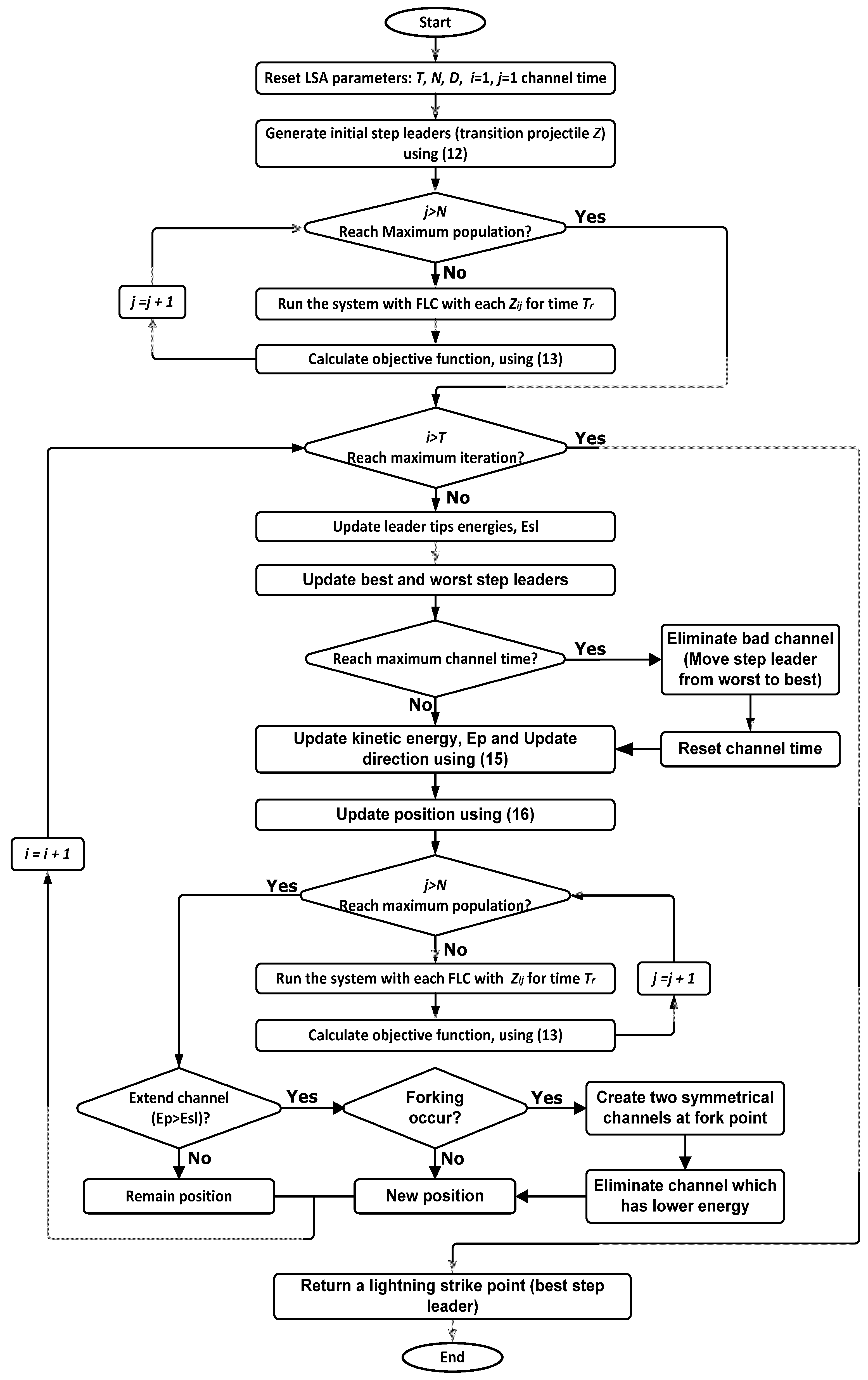
4.3. Implementation Steps of LSA to Obtain the Optimal FLC Design

The implementation starts by resetting the LSA parameters, namely, number of iterations (T), population size (N), problem dimension (D), and channel time. The initial populations for the MFs are then generated and encoded according to Equation (12). The next step involves the evaluation of the objective function through Equation (13). A suitable running time Tr is required to populate the FLC output for the evaluation of MSE in population N. After the initial population is evaluated, the direction and position are updated with Equations (15) and (16), respectively: After updating all the values of Zi,j in the population, the procedure re-evaluates the objective function, and the process continues to the next iteration. This updating and objective function reevaluation process is repeated until the maximum iteration count is reached, as explained in Figure 5.
p i _ n e w S = p i S ± e x p r a n d ( µ i )
p n e w L = p L + n o r m r a n d ( µ L , σ L )
where p i _ n e w S is the new space projectile, p i S is the old space projectile, and p n e w L is the new lead projectile. After updating all the values of Zi,j in the population, the procedure re-evaluates the objective function, and the process continues to the next iteration. This updating and objective function reevaluation process is repeated until the maximum iteration count is reached, as explained in Figure 5.

5. FLC Design for PV Inverter Control Using the Proposed Method

A 3 kW, 240 V, 50 Hz PV inverter system is modeled in the Matlab Simulink environment (Figure 6) to demonstrate the application of an optimum FLC design by supplying various types of loads continuously. As depicted in Figure 6, the output voltages (Va, Vb, and Vc) are measured and converted to Vd and Vq at each sampling time Ts = 2 µs. The controller block shown in the figure contains two FLCs that correspond to Vd and Vq in the d–q reference frame. The controllers require E and CE to generate new Vd and Vq and to convert to Va, Vb, and Vc. The converted signals are then utilized to create the PWM for driving the IGBT switches of the inverter.
As explained previously for each input, seven MFs defined as trapezoidal and triangular MFs are used according to the illustration in Figure 7. Seven parameters (i.e., X i , j 1   t o   X i , j 7 ) are used to define the first input (E), whereas the seven other parameters (i.e., X i , j 8   t o   X i , j 14 ) are used to define the second input (CE). Therefore, each controller input Z in the optimum FLC design contains 14 parameters. Thus, the FLC control rule for the PV inverter control system includes 49 rules (Table 1).
The input vector and control rules are then defined. The optimization process described in the previous section can be performed by evaluating the objective function given in Equation (13) with the Simulink model shown in Figure 6 for a suitable running time of Tr = 0.2 s. In this design illustration, the optimization process based on LSA is started by initializing the following parameters: the number of iterations (T) as 100, number of populations (N) as 20, dimension of the problem (D) as 14, and maximum channels as 10. After the creation of the initial population and the calculation of the corresponding objective function for each input vector in the population, LSA updates the population and initiates a new iteration. If LSA reaches the maximum iteration, then the FLC with the best MF is obtained (Figure 5). This result indicates that the proposed approach provides a systematic and easy way to design FLCs for PV inverter control systems.

6. Fuzzy Logic PV Inverter Controller Implementation Based eZdsp F28335

The implementation in the hardware of the developed optimized FLC for PV inverter using eZdsp F28335 control board is essential to appraise the performance of the controller in real time. Therefore, the implementation to test the optimized FLC-based PV inverter is performed in the laboratory.

6.1. eZdsp F28335 Controller

The eZdsp F28335 board is appropriate for the inverter control platform because of its ability to link the MATLAB/Simulink inverter model to the real-time hardware. It is an inexpensive standalone digital controller that contains an analog-to-digital converter (ADC), a digital input/output, and a TMS320F28335 floating-point DSP. In the controller, Code Composer Studio (CCS) and MATLAB/Simulink should be operated properly. The Simulink PV inverter model is compiled, converted to C-code, and then automatically linked to the real-time TMS320F28335 processor through MATLAB/Simulink. During the linking process, a user should include eZdsp input–output (I/O) interface blocks, such as ADC, and the enhanced PWM (ePWM) in the Simulink models. The behavior and performance of the inverter can be monitored in real time by applying the CCS software. The most important features of the eZdsp F28335 board include a TMS320F28335 digital signal controller, 150 MHz operating speed, 68 Kb on-chip RAM, 512 Kb on-chip flash memory, 256 Kb off-chip SRAM memory, and on-chip 12-bit ADC with 16 input channels. These components constitute the eZdsp F28335 board, which is suitable for prototype development and cost-sensitive, rapid-control prototyping.

6.2. Control Algorithm Implementation

The control algorithm described in Section 2 is implemented with the eZdsp F28335 board. This algorithm initially reads the measured voltages Va, Vb, and Vc through LEM LV25-P sensors. Therefore, three sensors are utilized to interface the output voltages of the inverter with the eZdsp F28335 board. These three sensors decrease the voltages to a level suitable for the eZdsp F28335 working voltages, and these voltages are fed to the ADC channels of the eZdsp F28335 for additional processing.
Va, Vb, and Vc are then transformed into the d–q reference frame, and E and CE are calculated in per unit according to Equations (6) and (7), respectively. The resulting E and CE are fed to the FLC to control the steady-state error and the output voltage.
Space vector PWM (SVPWM) is employed in the inverter control algorithm to produce sinusoidal AC waveforms from the three-phase voltage source inverter [30,31]. Each output signal cycle is divided into six sections that resemble a hexagon (Figure 8). Vref and α in each sector are the products of two adjacent nonzero and zero vectors, respectively. The hexagon consists of six nonzero vectors, namely, V1, V2, …, V6, and two zero vectors, particularly V0 and V7 [32]. The PWM control includes the modulation index (MI), which is necessary to improve the accuracy by decreasing the total harmonic distortion (THD) of the output signals from the inverter [33]. The MI is computed as follows:
M I = V p 1 V p 1 s i x
where Vp1 is the maximum fundamental voltage, and Vp1six is the maximum fundamental voltage through a six-step operation. Thus, V p 1 six = 2 π V dc , where Vdc is the DC-link voltage [30]. The remainder of Ts is filled with the zero space vectors V0 and V7. The time shares are calculated as follows [34]:
T 1 = 3 · T s · | V r e f | V d c sin ( n 3 π α )
T 2 = 3 · T s · | V r e f | V d c sin ( α n 1 3 π )
T 0 = T s ( T 1 + T 2 )
where n = 1 to 6 are the sectors at 0 ≤ α ≤ π/3; T1, T2, and T0 are the time vectors of the respective voltage vectors; Ts is the switching time; and α is the angle of the reference vector relative to the space vector.
The inverter uses the optocoupler in the driver circuit to establish the interface of the SVPWM to the IGBT. The voltage values of the produced SVPWM switching signals are appropriate for the IGBT working voltage to achieve an effective inverter switching operation.

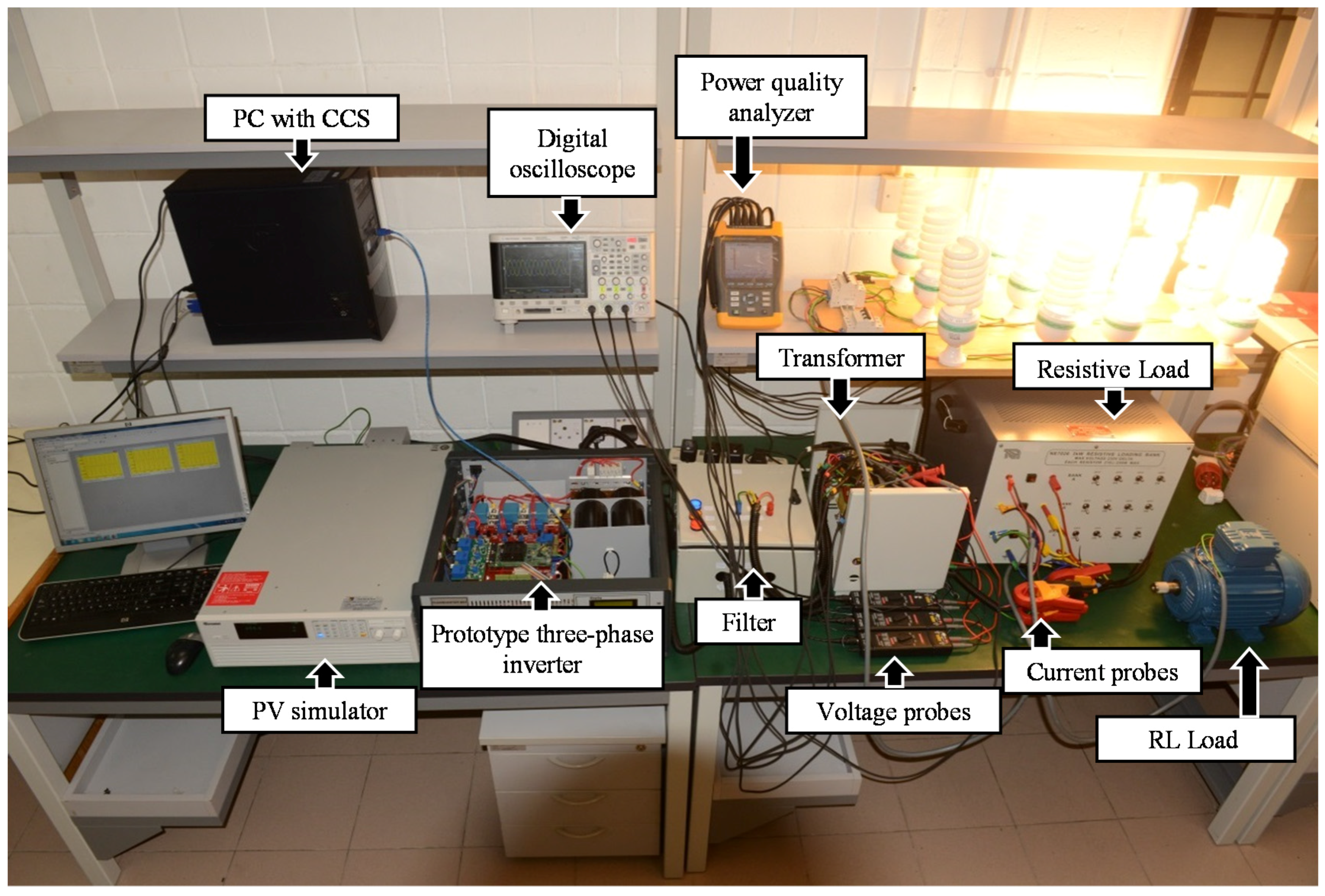
7. Experimental PV Inverter Control System

The real-time model shown in Figure 9 is utilized to implement the PV inverter control system through eZdsp F28335 board. In this model, the employed eZdsp F28335 I/O blocks include C280x/C28x3x ADC, unit16, and C280x/C28x2833x ePWM. The inverter output voltages, particularly Va, Vb, and Vc, are sampled via C280x/C28x3x ADC. These voltages are then converted to digital values for processing. The C280x/C28x2833x ePWM block produces the PWM switching signals for the IGBTs.
Referring to Figure 9, the first block is the ADC C280x/C28x3x. The ADC module which has 16 channels, is configurable as two independent 8-channel modules (module A and module B) to service the ePWM modules. The two independent 8-channel modules can be cascaded to form a 16-channel module. Multiple input channels and two sequencers are available with only one converter in the ADC module. The two 8-channel modules can auto sequence a series of conversions with each module having the choice of selecting any one of the respective eight channels available through an analog MUX. In the cascaded mode, the auto sequencer functions as a single 16-channel sequencer. On each sequencer, once the conversion is completed, the selected channel value is stored in its respective ADCRESULT register. Auto sequencing allows the system to convert the same channel multiple times. Functions of the ADC module include a 12-bit ADC core with built-in dual sample-and-hold (S/H), and analog input from 0 V to 3 V. The analog input for the ADC is in the range of 0 to 3 V. As the ADC is 12-bit, the digital value of the input analog voltage is calculated as:
D i g i t a l   V a l u e = { 0 i n p u t 0   V 4096 × I n p u t   A n a l o g   V o l t a g e 3 0   V < i n p u t < 3   V 4095 i n p u t 3   V
From Equation (21), the digital output is from 0 to the 4095. To remove the bias from the digital signal and get the actual signal, it must be subtracted from half of the highest value (4095). Experimentally, the half of the highest value is found to be 2058. As the control procedure is working in per unit (p.u.), therefore the actual signal should be converted to p.u. signal. The actual signal should be divided by the highest value for converting to p.u. signal. Therefore, the actual signal is dived by 1240 to get the p.u. signal.
The C280x/C28x2833x ePWM block is one of the most important blocks in the eZdsp F28335 control board for PV inverter control. As shown in Figure 9, three ePWM blocks are used. Each ePWM block is responsible to generate the switching for the switching devices (IGBTs) in each inverter leg. The dead-time which is the time delay between the upper switch (e.g. IGBT1) turning ON time and lower switch (e.g. IGBT4) turning OFF time should be taken into account. The dead-band sub-module supports independent values for rising-edge (RED) and falling-edge (FED) delays. The amount of delay is programmed using the dead-band RED (DBRED) and dead-band FED (DBFED) registers. Since the DBRED and DBFED are 10-bits, they can be set to values from 0 to 1023. The rising-edge-delay and falling-edge-delay can be calculated as:
R E D = D B R E D C P U   c l o c k
F E D = D B F E D C P U   c l o c k
where DBFED is the dead-band FED and DBRED is the dead-band RED.
In the experiment, 25 SolarTIFSTF-120P6 PV modules with a peak capacity of 3 kW are utilized to supply the load. The modules are subsequently arranged in a series-connected configuration; thus, a DC output voltage of 435 V is produced. The characteristics of the SolarTIFSTF-120P6 PV module are shown in Table 2. Solar irradiation and temperature are the two main parameters responsible for the output power of the solar cell. The mathematical model of the PV electrical circuit is represented by the output of the cell current, which is obtained as follows [35,36,37,38]:
I P V = I p h I o ( e ( q ( V + I .   R s n . K B . T ) 1 ) V + I . R s R s h
where IPV is cell output current (A), Iph is the light-generated current (A), Io is the cell reverse saturation current or dark current (A), q is the electronic charge (1.6 × 10⁻¹⁹ C), V is the cell output voltage (V), n is the ideality factor, KB is the Boltzmann’s constant (1.38 × 10⁻²³ J/K), T is the cell temperature (K), and RS is the internal resistance of the stack.
The short-circuit current Isc,n under the nominal condition and that at the short-circuit current temperature coefficient α are provided in Table 2. The PV characteristics are programmed in the PV simulator Chroma 62050H-600s to represent the actual variation of voltage and current.
In the inverter input stage, the configuration of the PV modules in series, parallel, or combination is responsible for the current IPV and voltage VPV of the PV system. In the proposed PV system, IPV and VPV are expressed as follows:
V P V = N S [ V r e f β ( T T n ) R s ( T T n ) ]
I P V = N P [ I r e f α ( T T n ) G G n + I S C ( G G n 1 ) ]
where NS is the series module number, Vref is the PV reference voltage, β is the voltage temperature coefficient, T is the stack temperature, Tn is the nominal temperature, NP is the parallel module number, Iref is the PV reference current, G is the irradiance, and Gn is the nominal irradiance. The inverter prototype is developed and verified on based on the experimental setup shown in Figure 10.

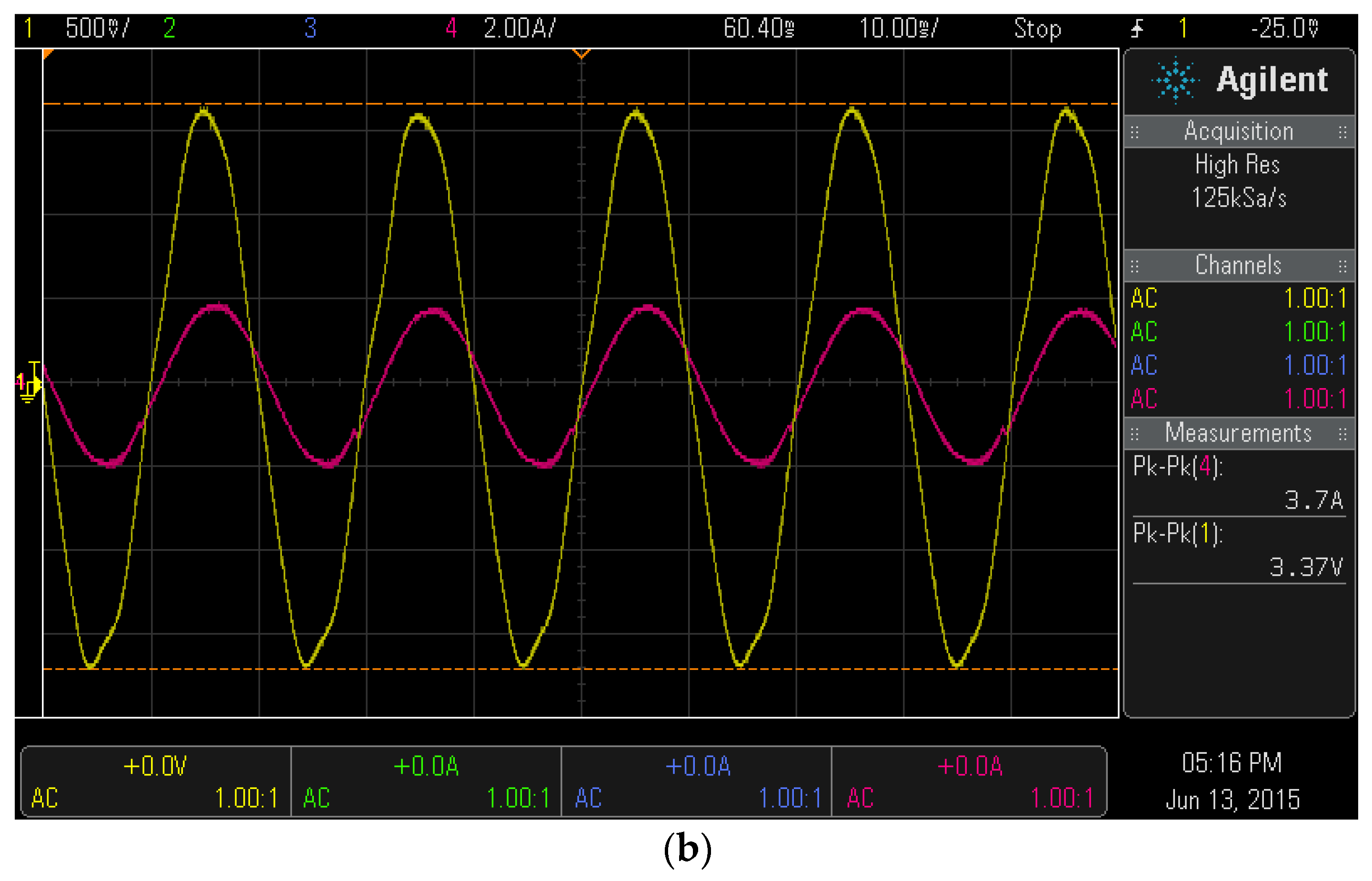
8. Results and Discussion

The PV inverter system depicted in Figure 6 is used to evaluate the proposed LSA-based FLC (LSA-FL) optimization method and the robustness of the overall system. Figure 11 shows the convergence characteristics of LSA-FL to determine the best optimal solution for the test system, along with the results obtained with DSA-based FLC (DSA-FL) and PSO-based FLC (PSO-FL) optimization methods. For a fair comparison, all optimization algorithms used the same parameters (i.e., problem dimension, population, and iteration). Figure 11 shows that LSA-FL converges faster than DSA-FL and PSO-FL. The optimal solution generated with LSA-FL is also better than those generated with DSA-FL and PSO-FL. The optimum performance of LSA-FL shown in Figure 11 is obtained when both FLCs that represent Vd and Vq accomplish the MFs shown in Figure 12. In consideration of its effectiveness, only FL-LSA is used to evaluate the performance of the overall PV inverter system when subjected to different types of loads.

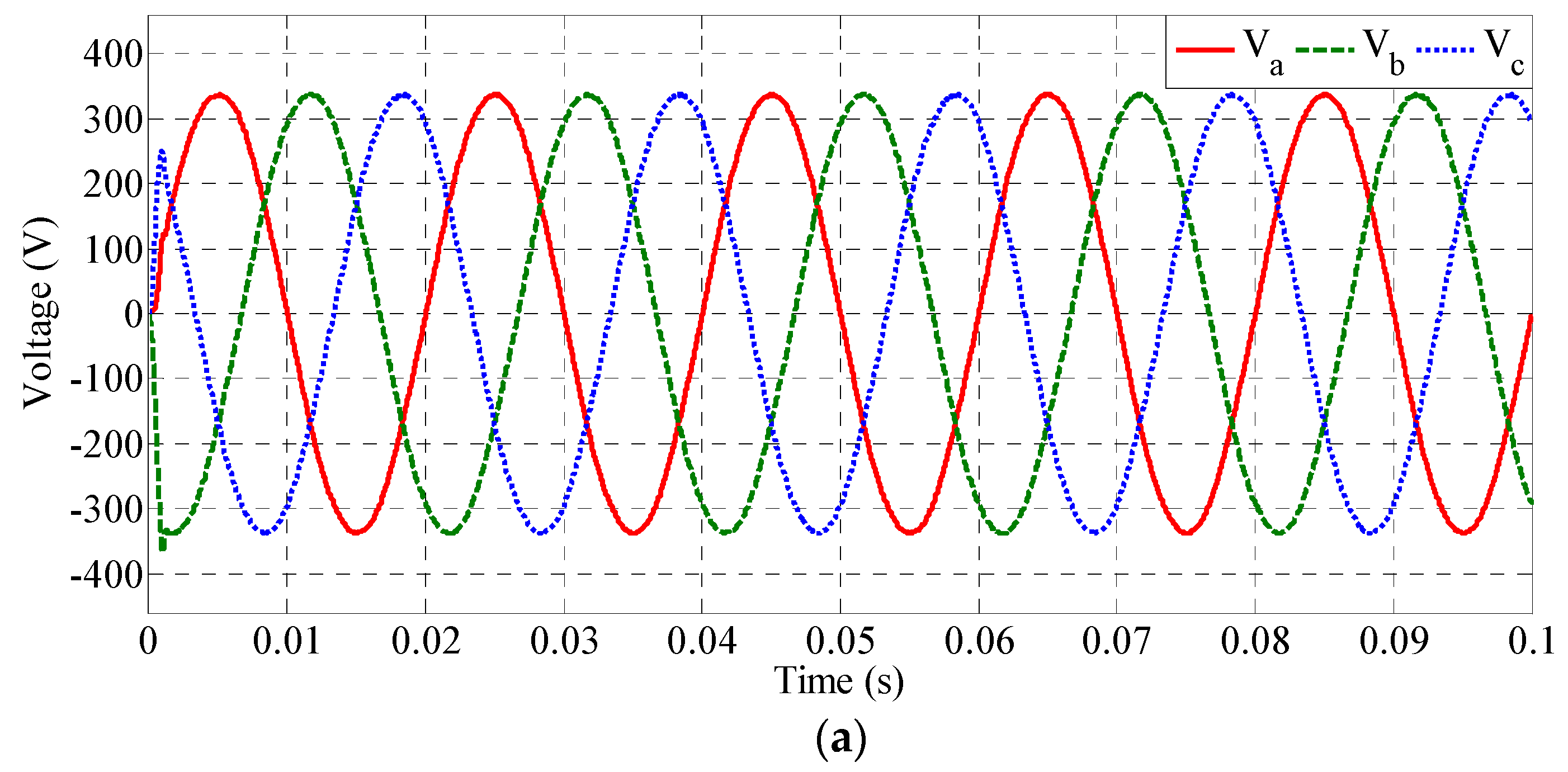
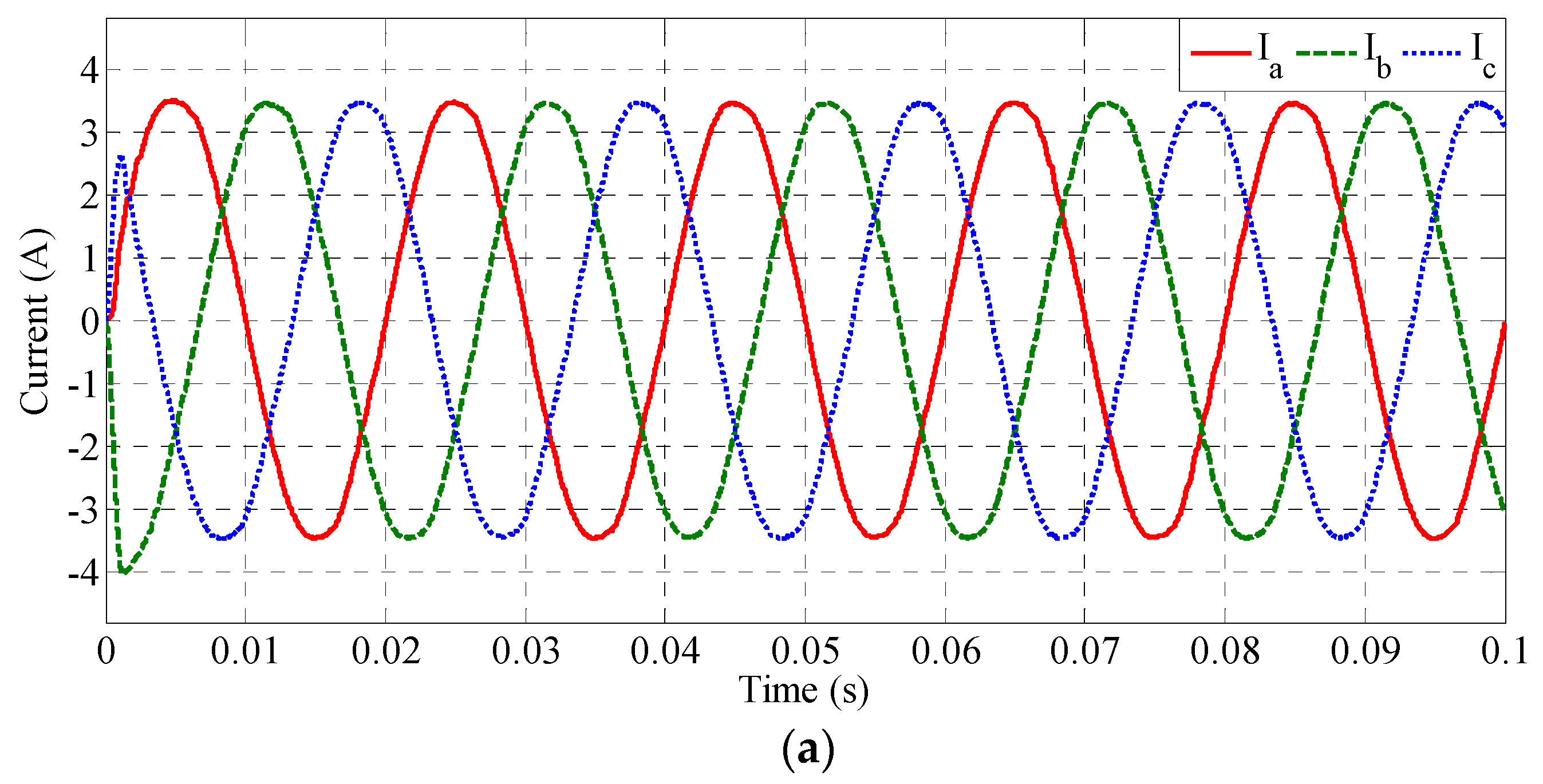
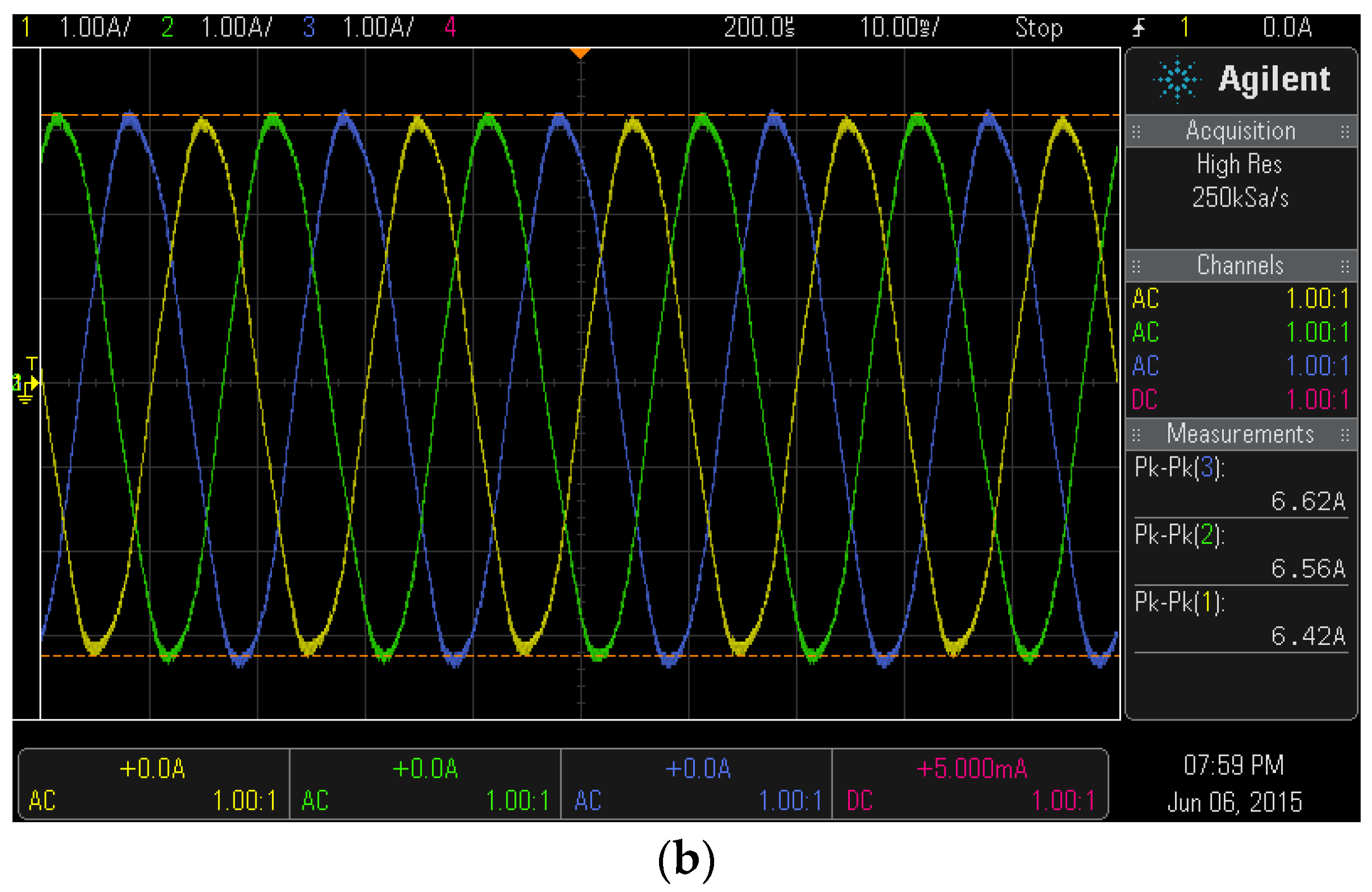
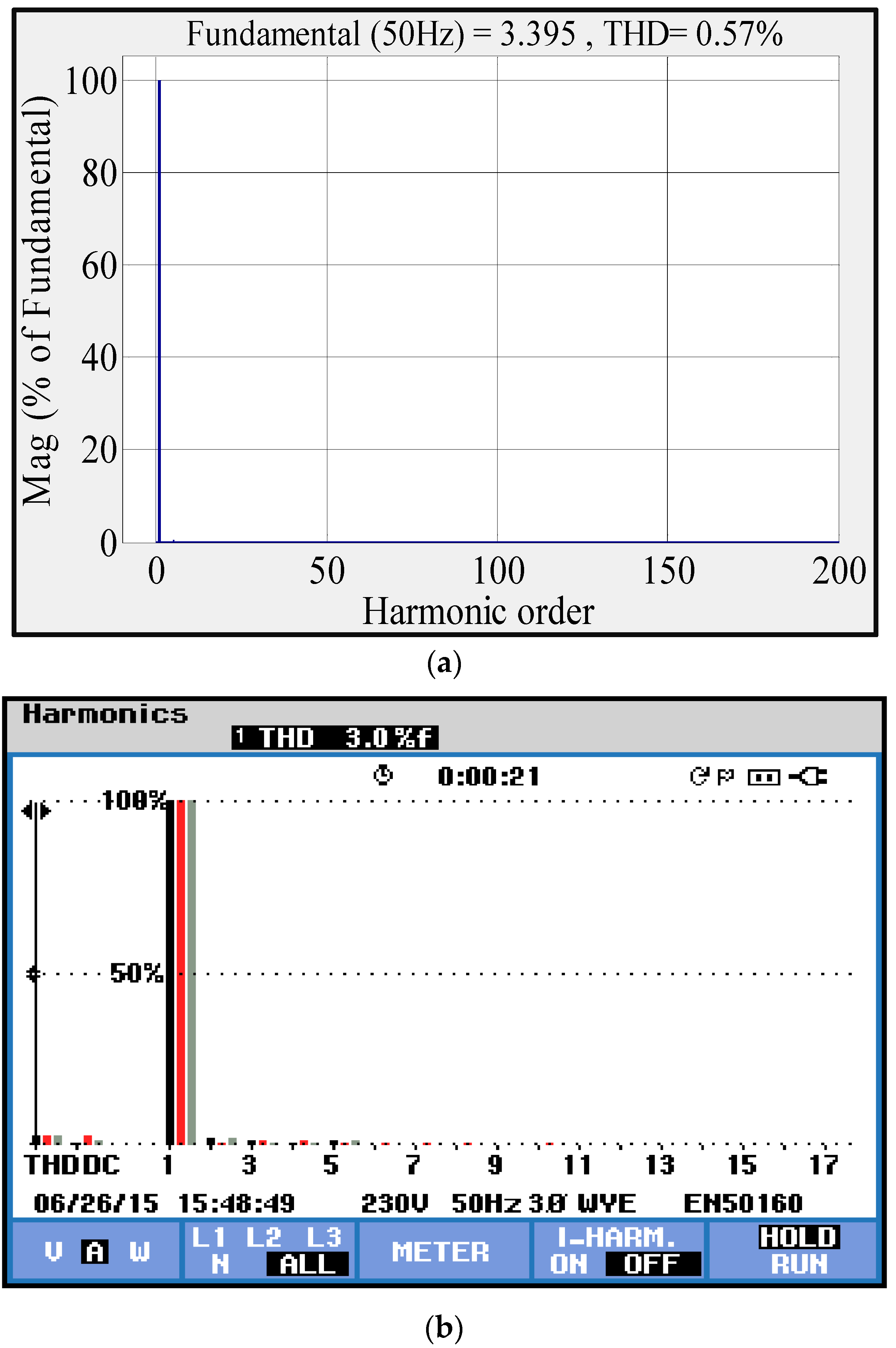
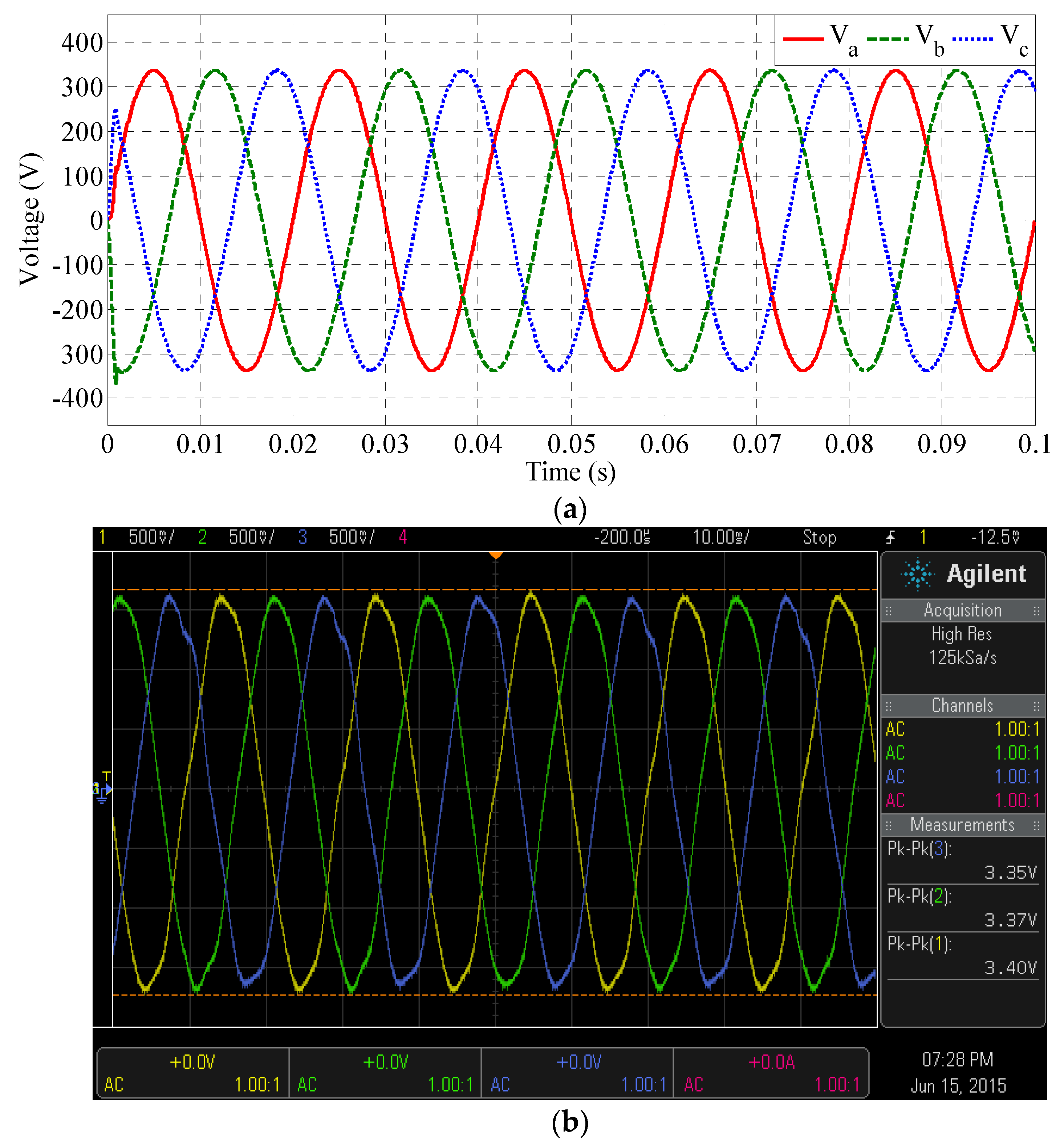
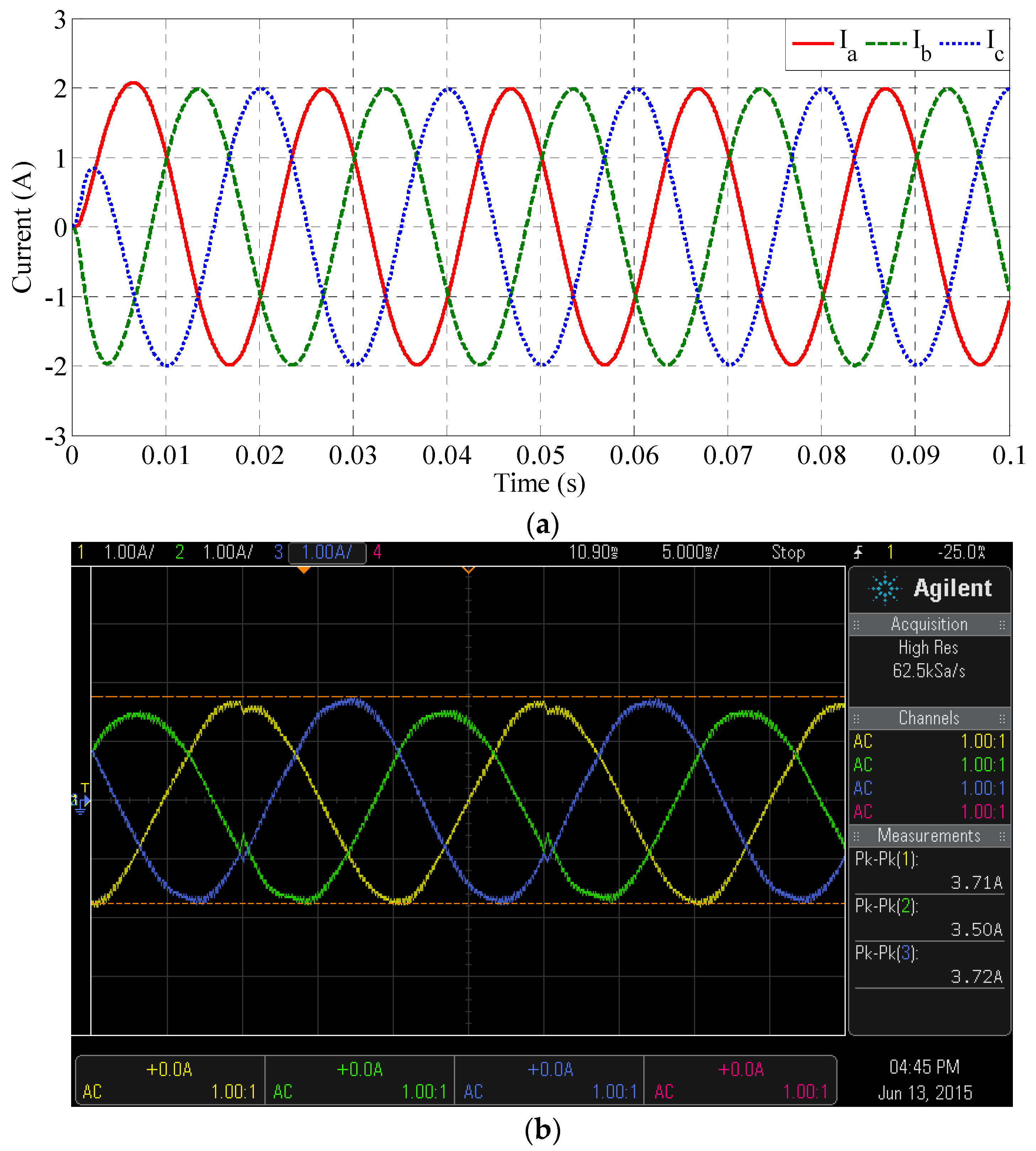
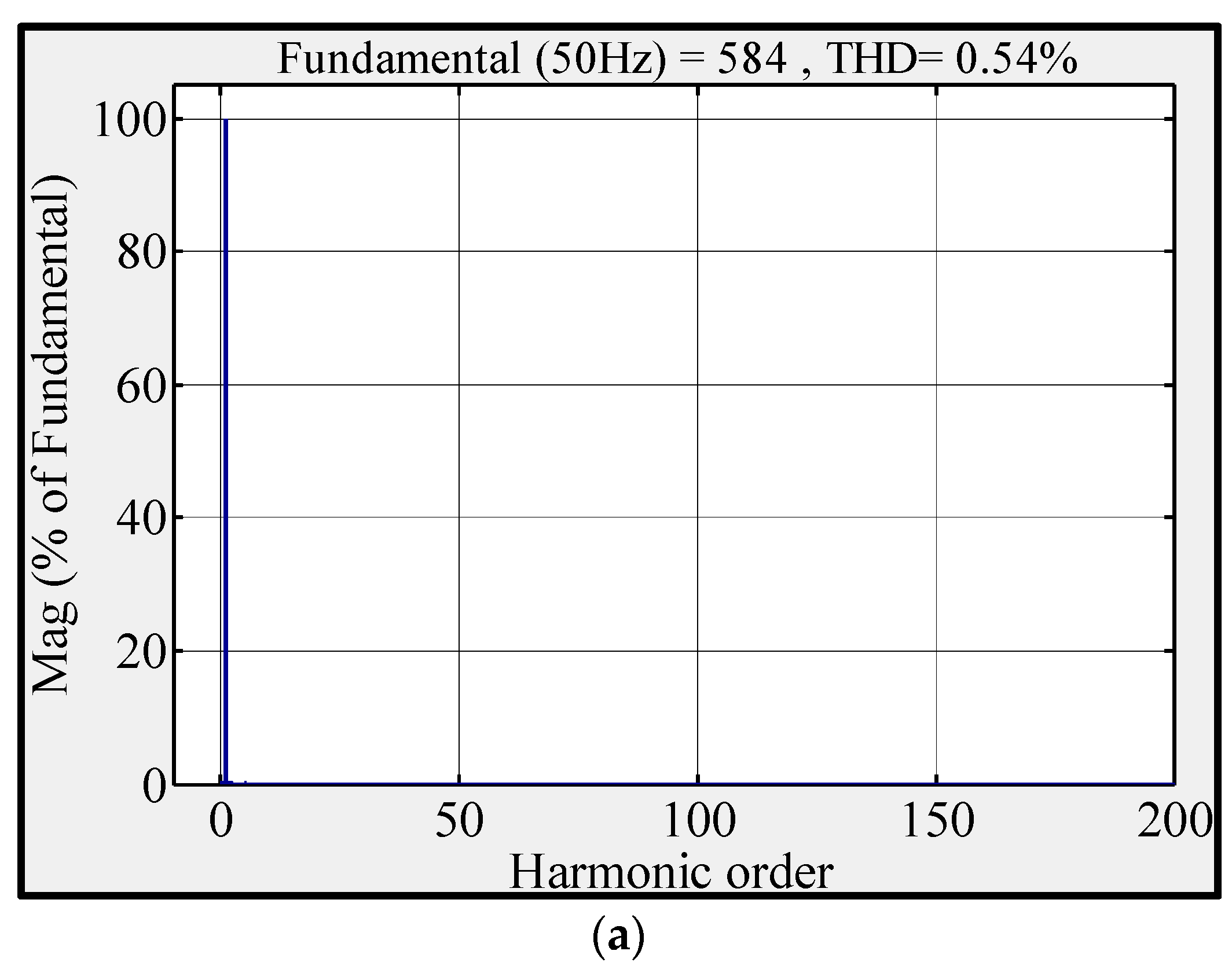
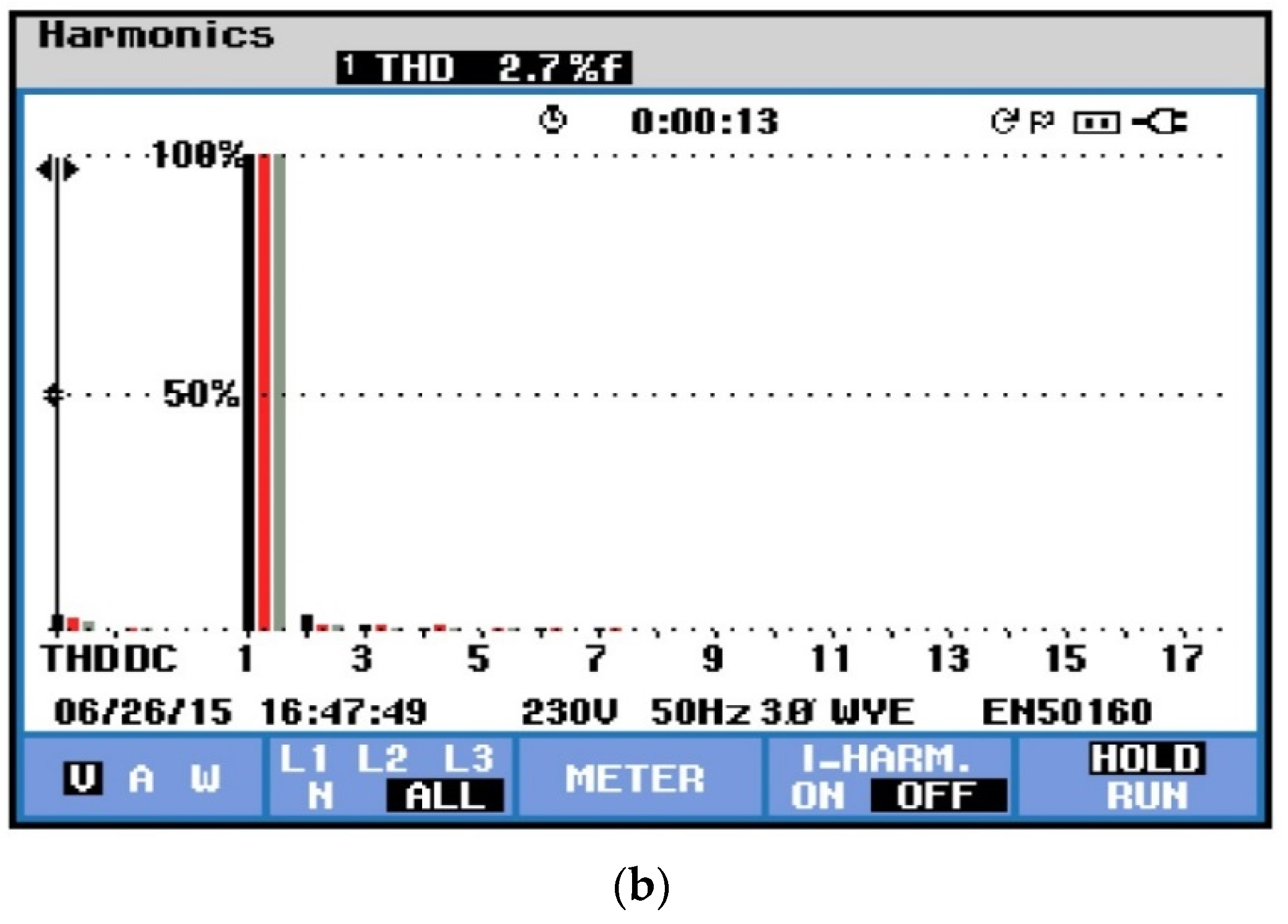
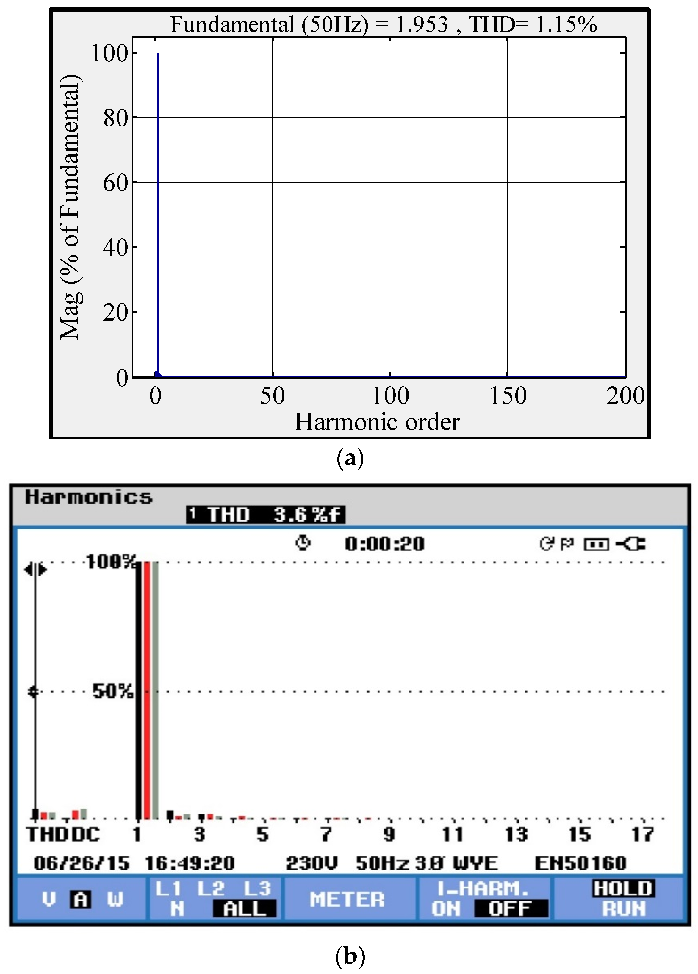
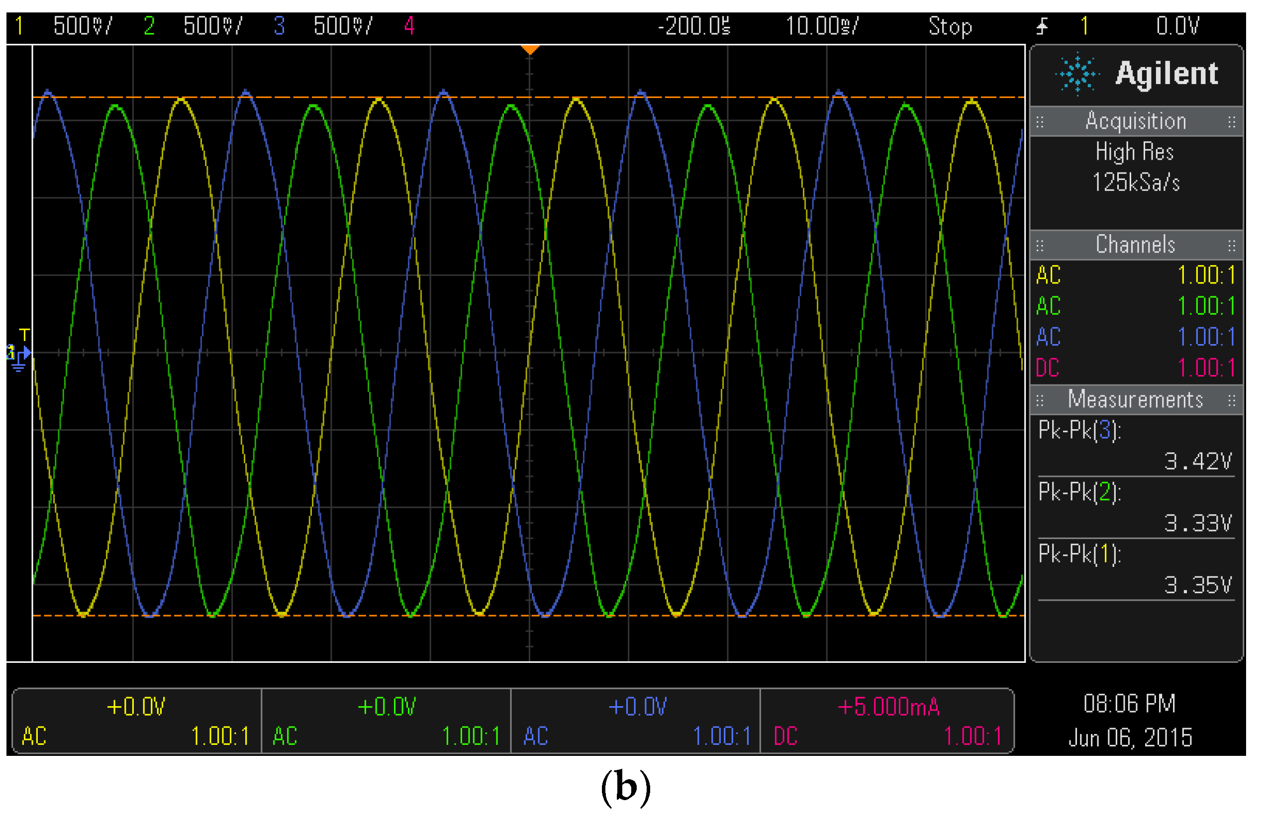
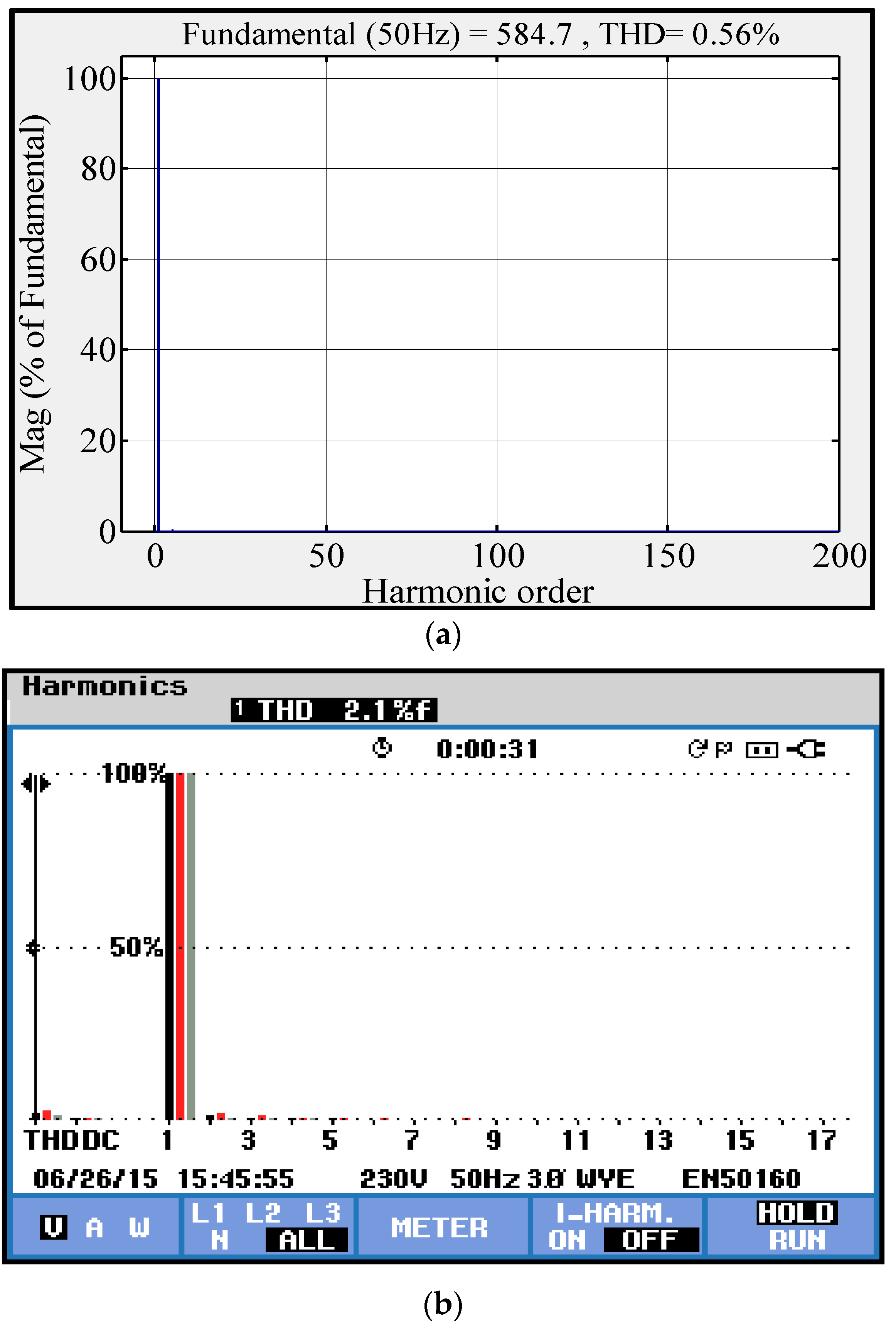
8.1. Results with Resistive Load (R)

A simulation is conducted with a resistive load of 1500 W for 0.1 s as can be shown in Figure 13a. Furthermore, the experiment is conducted in the laboratory to evaluate the overall performance of the proposed fuzzy logic PV inverter controller. Experimental voltage waveforms are measured with differential probes with a scale (X200), as depicted Figure 13b.
Both the simulation and experimental output voltage waveforms of the inverter, namely, Va, Vb, and Vc, are sinusoidal with 50 Hz, and no negative effect exists, such as overshoot or oscillation. The shift is 120° between each phase. The controller distinctly succeeds in regulating the magnitude of the phase voltage waveform at approximately 339 V and the rms voltage of 240 V. This result confirms that the proposed FLC is in accordance with the exact voltage reference; therefore, the proposed inverter control algorithm is efficient. The three-phase load current waveforms should also be recorded analysis. The load current waveforms are measured, as shown in Figure 14. Similar to the three-phase output voltage waveform, the phase load current waveforms in the simulation and the experimental are successfully regulated through the proposed controller within approximately 3.3 A. The load current waveforms are purely sinusoidal with 50 Hz, and a 120° shift is demonstrated between each phase.
Power factor is essential for the three-phase inverter design to indicate the efficiency of the proposed inverter and its control algorithm. The goal of the design is to obtain a unity power factor. Therefore, the voltage and the load current waveforms are measured simultaneously (Figure 15) to depict the phase difference between these signals. The voltage and the current waveforms exhibit the same phase angle, which is in accordance with the unity power factor operation, as expected. The phase relationship of load current and voltage signals in the simulation and the experimental indicates high efficiency (Figure 15).
The THD of the voltage and current signals are measured in the simulation and the experimental to verify the quality of the inverter output waveforms. The quality of the waveform is inversely proportional to the THD percentage. Figure 16 and Figure 17 show the THD percentages of the voltages and currents obtained for the R load analyzed in this study. Figure 16a,b shows that the THD of the voltage waveform is 0.56% and 2.1% for the simulation and the experimental, respectively, which satisfies the IEEE-929-2000 international standard [39].
Figure 17a,b shows that the THD of the current waveform is 0.57% and 3% for the simulation and the experimental, respectively, which complies with the IEEE-929-2000 international standard. The low THD in the voltage and current waveforms is mainly achieved with the robustness of the proposed FLC. Two tests are conducted to appraise the proposed fuzzy logic PV inverter controller. The robustness and efficiency of any controller are indicated prominently when perturbation occurs in DC input voltage or when a change in the value of load occurs. Therefore, two tests were performed, namely, changing R load and changing DC input voltage, to determine the validity and ability of the proposed fuzzy logic PV inverter controller.

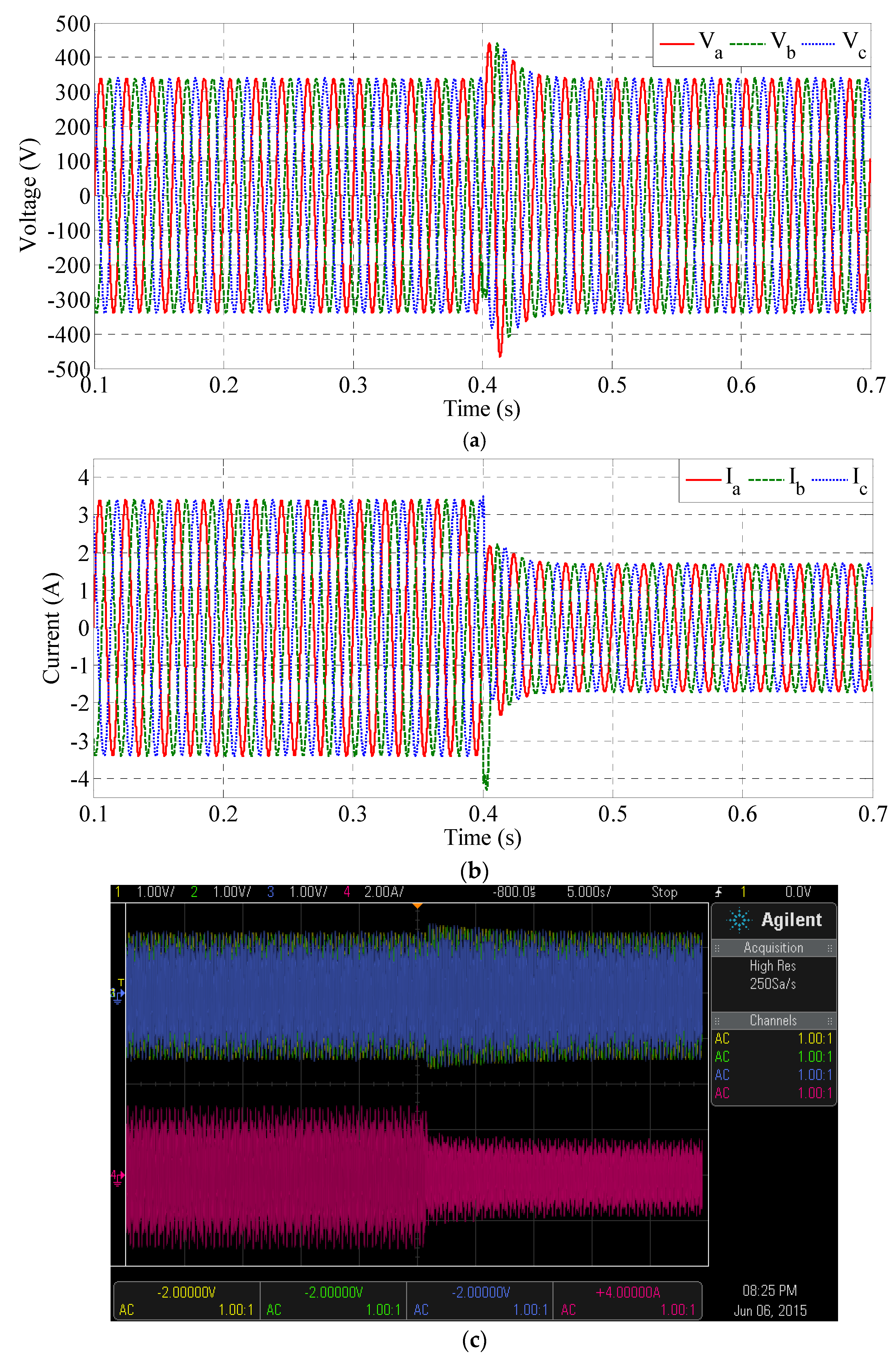
8.1.1. Step Change in R Load

The effect of a large step change in the load should also be investigated. A change in the load usually disturbs the voltage, and the controller regulates this disturbance by controlling the MI. The load decreases from 1500 W to 750 W at 0.4 s. Figure 18a,b illustrates the simulation voltage and current signals, respectively. Meanwhile, Figure 18c illustrates the experimental voltage and current signals. Figure 18 illustrates that the decrease in load results in an increase in output voltage waveform, which changes the E and CE signals. The controller possibly detects these signals, and suitable control signals are supplied to regulate the inverter output waveforms.
Figure 19a,b illustrates the simulation voltage and current, respectively, for load that increases from 750 W to 1500 W at 1 s. Figure 19c shows the experimental voltage and current signals. The change in the load disturbs the voltage and the current waveforms.
The controller regulates the inverter output waveforms successfully. Therefore, the inverter output responses indicate that the proposed controller is sufficiently robust to achieve a favorable response to a change in step load.

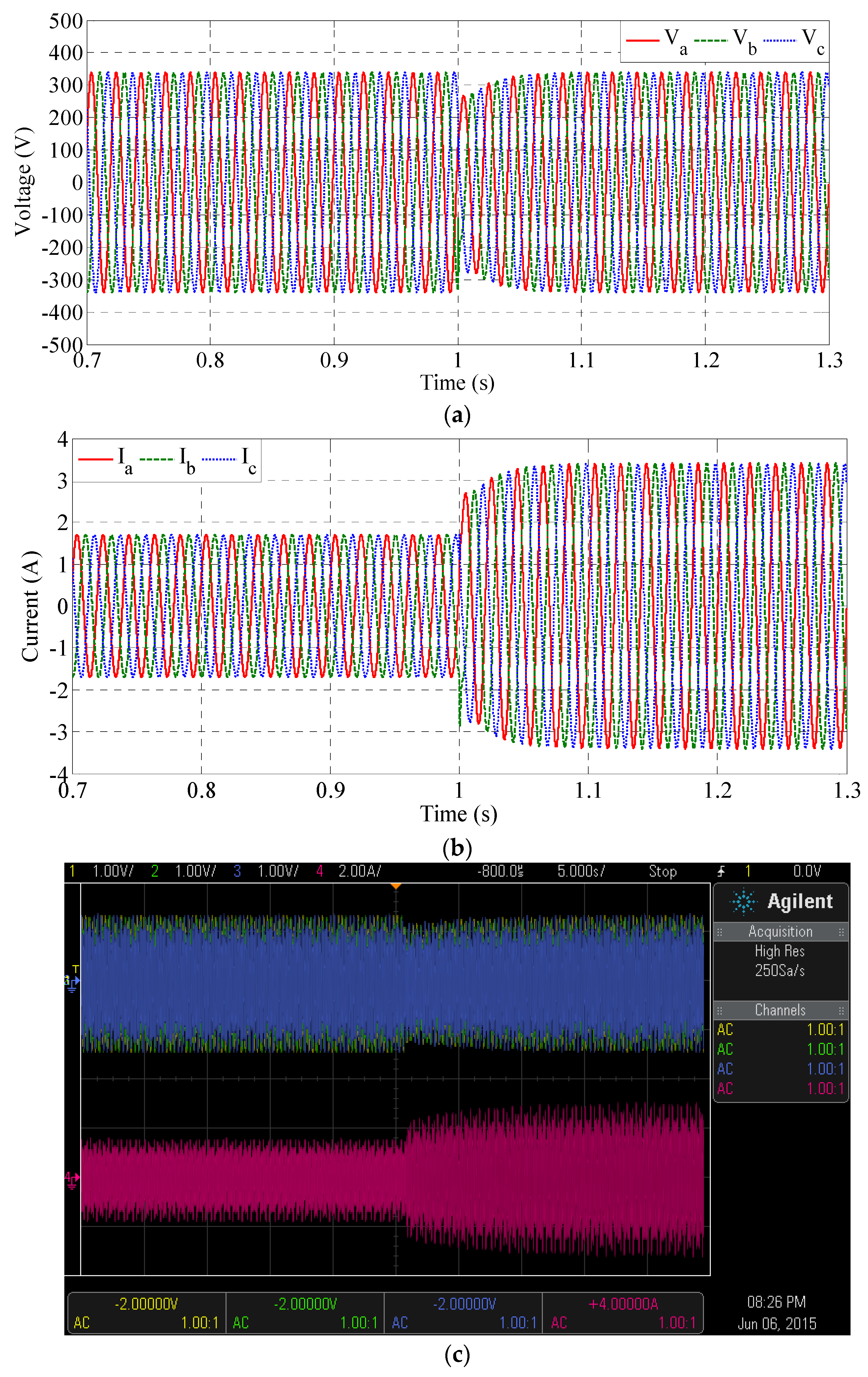
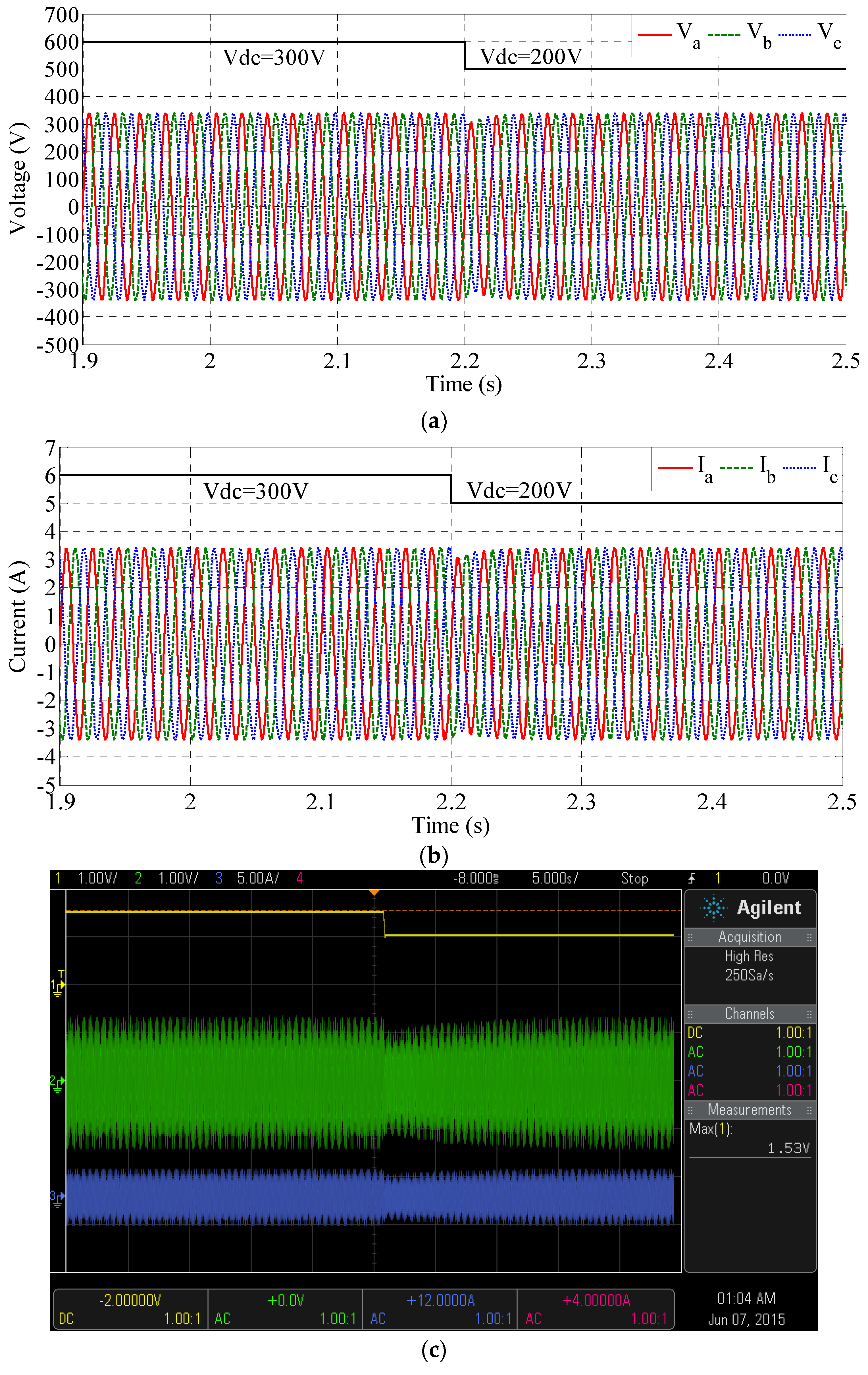
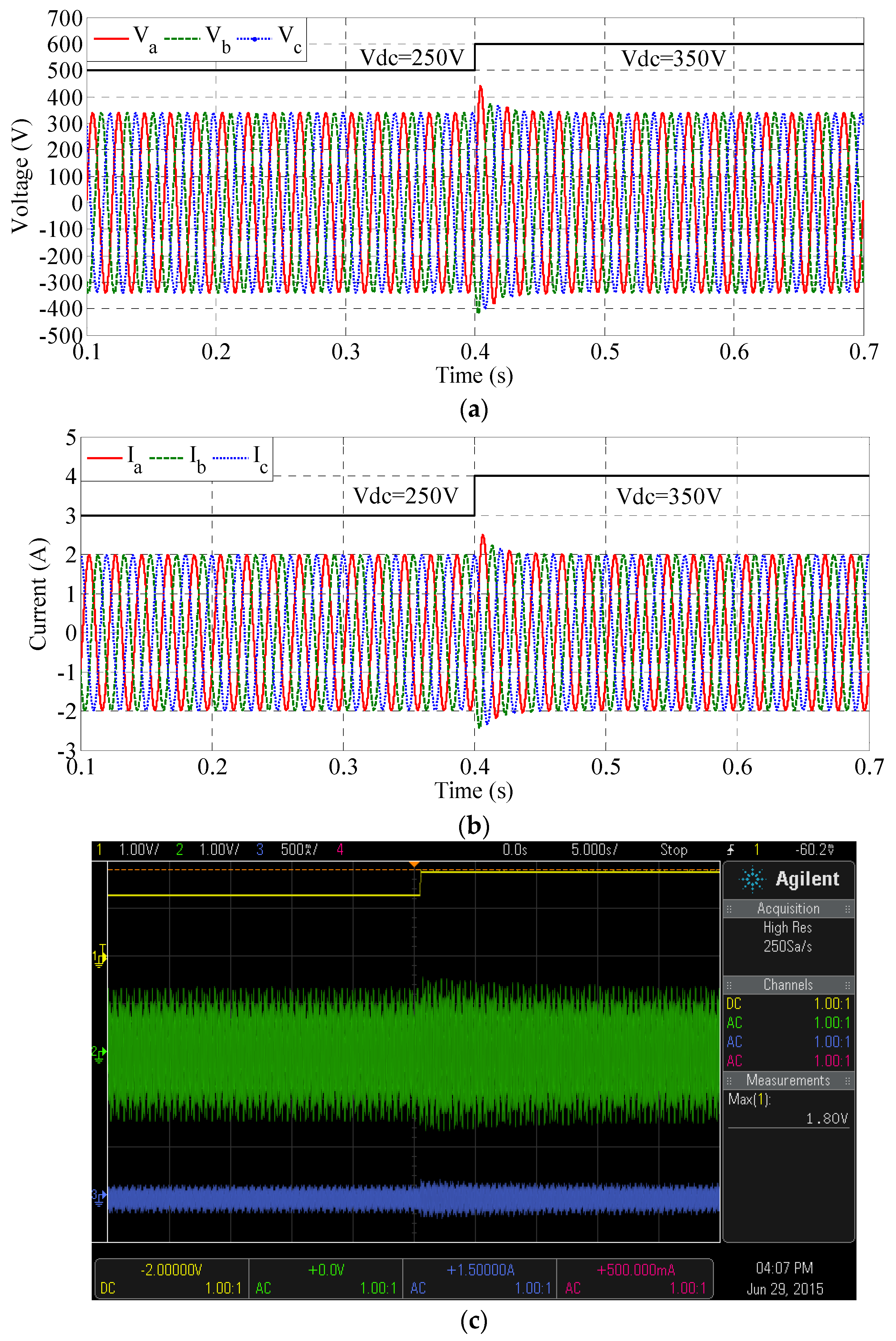
8.1.2. Step Change in Vdc

The intermittent PV characteristics should be appraised to determine the effectiveness of the proposed controller. The PV system suffers from a fluctuating DC voltage. Therefore, the change in the step DC voltage, Vdc, should also be examined to analyze the proposed controller. Vdc is increased from 200 V to 300 V at 1.6 s to test the proposed controller. Figure 20a,b illustrates the voltage and current waveforms, respectively. Meanwhile, Figure 20c illustrates the experimental voltage and current signals. An increase in Vdc also increases the voltage and current waveforms. Therefore, the proposed controller regulates the inverter output waveforms successfully; thus, the proposed controller is implemented successfully.
Vdc is decreased from 300 V to 200 V at 2.2 s to evaluate further the proposed controller. The voltage and current waveforms are illustrated in Figure 21a,b, respectively. Meanwhile, Figure 21c shows the experimental voltage and current waveforms. The decrease in Vdc decreases the inverter voltage and current output waveforms. The proposed FLC successfully regulates the voltage and current waveforms. This finding indicates that the proposed controller can deal with the change in Vdc with different loads, and it can be efficiently used in PV systems.

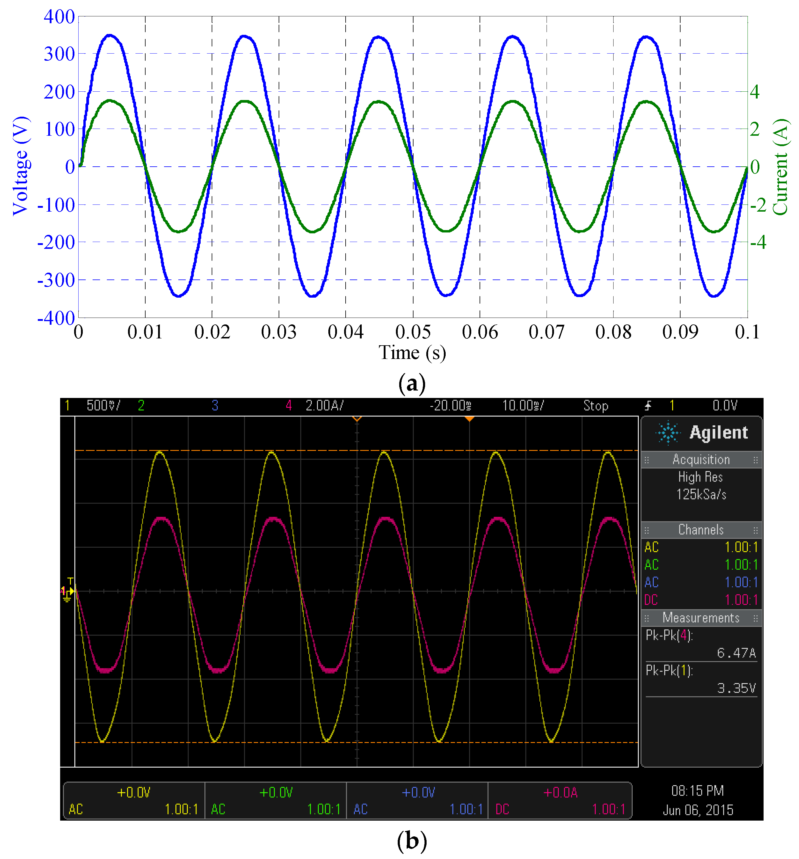
8.2. Results with Resistive and Inductive Load (RL)
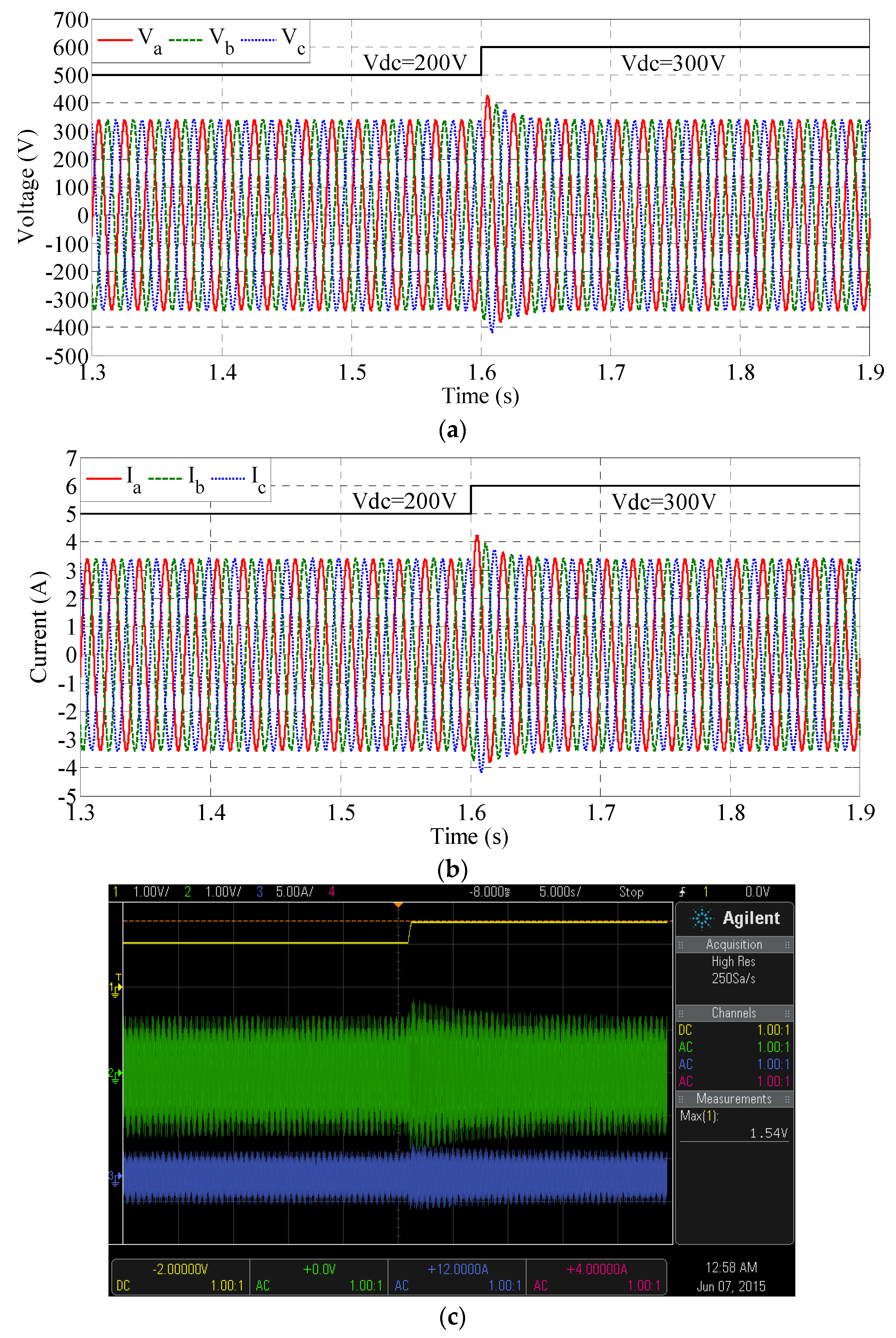
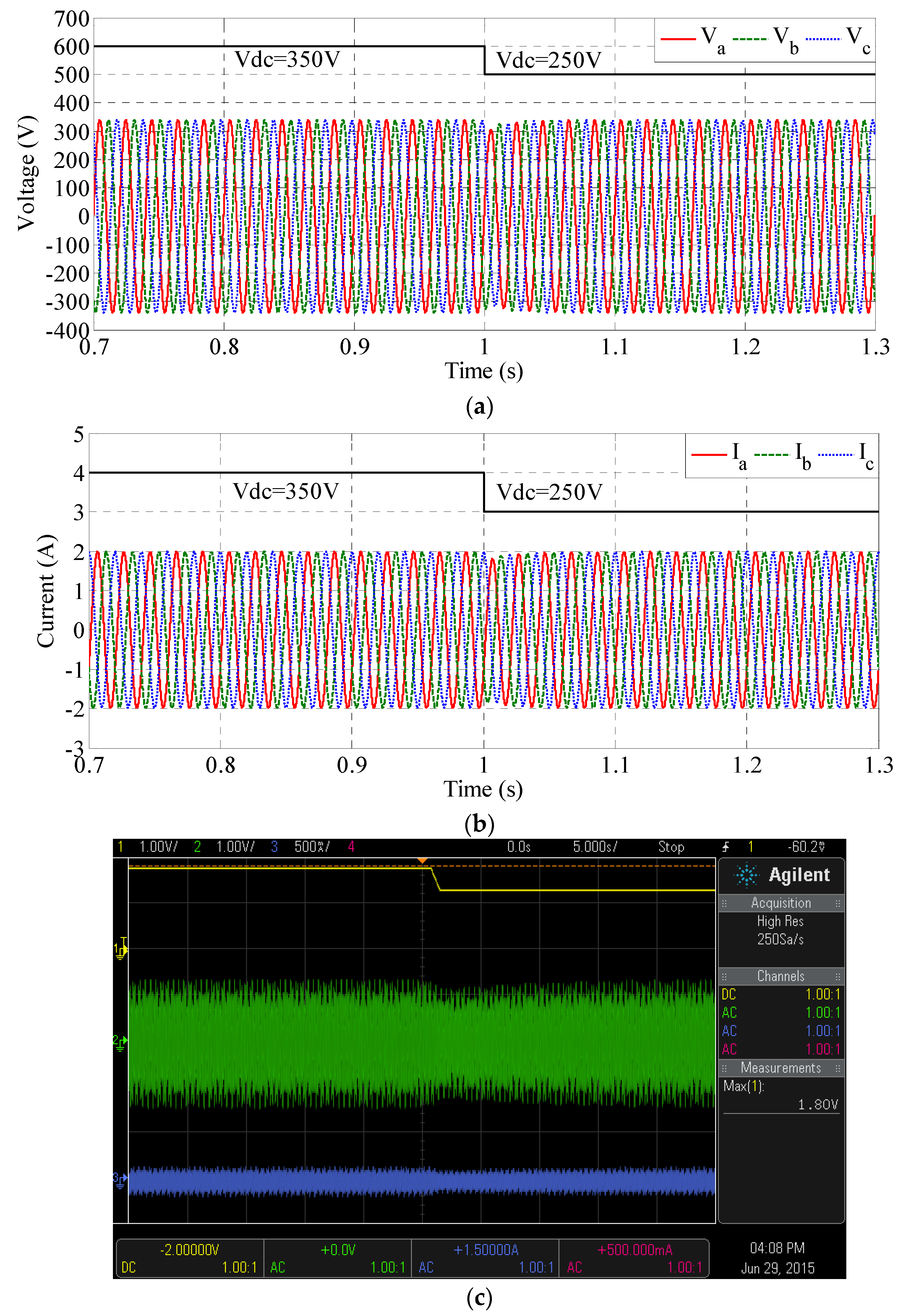
Another type of load is used to test the robustness of the controller. In this case, RL load represented by a motor with a capacity of 1 hp is used. The equivalent circuit for this motor is equal to (89.9161 + j57.509). Therefore, the values of the RL load are R = 89.9161 Ω and L = 183.1 mH. The simulation is performed for 0.1 s, as depicted in Figure 22a. Figure 22b shows the experimental voltage waveforms of the three-phase inverter, namely, Va, Vb, and Vc. The voltage waveforms are not affected by a change in the load type. The controller still succeeds in preserving the magnitude of the AC voltage signals for the three-phase inverter at approximately 339 V. The waveforms are stable, clean, and balanced at 50 Hz. The displacement between each two phase is 120°.
The simulation and experimental three-phase load current waveforms are presented in Figure 23a,b, respectively, to observe the effect of RL load on the current waveform. The change in load type does not affect the quality of the current waveforms. The waveforms remain stable, and the controller achieves a constant peak level with approximately 1.95 A and an approximately 1.37 A·rms. The waveforms remain balanced at 50 Hz, and they are displaced by 120° between each two phases.
The phase shift between the voltage and current with RL load is also measured to evaluate the controller further. Figure 24a,b illustrates the simulation and experimental output voltage (Va) and current load (Ia). The figure indicates that the power factor of the RL load is 84.2%, which means that the load current lags behind the voltage waveform by 32.6°.
The THD for the inverter output waveforms are also measured to verify the quality of the signals when the inverter is connected with RL load. Figure 25a,b shows the voltage THD for the simulation and the experimental. Figure 25 clearly shows that the controller succeeds in maintaining the voltage THD at a small percentage of 0.54% and 2.7% for the simulation and the experimental, respectively. The current THDs for the simulation and the experimental are shown in Figure 26. The controller also succeeds in maintaining the current THD of 1.15% and 3.6% for the simulation and the experimental, respectively. This finding indicates that the controller can successfully deal with RL load, and clean waveforms can be supplied, thereby meeting the IEEE-929-2000 international standard.

Step Change Vdc

The step change in Vdc is also implemented for RL load to appraise the robustness of the proposed FLC controller. Vdc is increased from 250 V to 350 V to determine the effect of a step change in the DC on the inverter output waveforms when the inverter is connected to an RL load. Figure 27 shows the inverter response with DC step change. Figure 27a,b illustrates the simulation voltage and current signals when Vdc increased from 250 V to 350 V at 0.4 s. Meanwhile, Figure 27c shows experimental voltage and current waveforms.
Figure 27 shows that the DC step change leads to an increase in voltage and current waveforms. In this case, the controller succeeds in regulating the inverter output waveforms, and the effect of the overshoot is limited with a short time. Figure 28a,b illustrates the voltage and current signals when Vdc changes from 350 V to 250 V at 1 s with RL load. Figure 28c shows the experimental voltage and current waveforms. Figure 28 clearly shows that the proposed FLC controller succeeds in regulating the voltage and current waveforms with a slight drop. Figure 28 indicates that the proposed FLC can also effectively deal with RL load with high efficiency.

9. Conclusions

This paper has presented a novel nature-inspired optimization technique called as the LSA to enhance the performance of the three-phase PV inverter and its practical implementation using the eZdsp F28335 controller board. The LSA is applied to optimally tune the MFs of the FLC based PV inverter instead of manual tuning. To optimize the MFs of the FLC, a suitable objective function is formulated by minimizing the MSE of the inverter output voltage. A comparative study with DSA and PSO techniques was performed to validate and compare the performance of the LSA. The simulations results showed that the FLC with optimally tuned MFs using the LSA performs well in tracking the reference value and regulating the output voltage waveforms at the desired amplitude for various loads. In addition, the LSA gives better results with high convergence rate compared to the DSA and PSO techniques.
To demonstrate the functionality of the proposed method, a hardware prototype of the optimal FLC based PV inverter is developed and compiled using the eZdsp F28335 controller board. The real-time model for the optimized FLC using LSA was first developed in the MATLAB environment to generate PWM switching signals for the IGBTs of the inverter. Thereafter, the developed controller was implemented in hardware using the eZdsp F28335 controller board in a prototype three-phase voltage source inverter. The developed PV inverter model was compiled, converted to the C-code, and automatically linked to the real-time TMS320F28335 processor board. The performance and behavior of the inverter was monitored in real-time by developing a GUI program in the CCS software. The experimental results with the prototype PV inverter showed that the proposed controller successfully regulated the inverter output waveform when connected to the resistive and combined resistive and inductive loads and also demonstrated the ability to handle changing DC input voltage and changing load. High quality inverter output voltage waveforms were obtained with low voltage THD values of 2.1% and 2.7% for the resistive and combined resistive and inductive loads, respectively. Furthermore, low current THD values of 3% and 3.6% are obtained for the resistive and resistive inductive loads, respectively. Therefore, the developed prototype optimum fuzzy logic based PV inverter controller implemented using the eZdsp F28335 control board is considered a useful device to be use in stand-alone and grid-connected PV systems.

Acknowledgments

The authors are grateful to Universiti Kebangsaan Malaysia for supporting this research financially under grant no. ETP-2013-044.

Author Contributions

Ammar Hussein Mutlag is a PhD student implementing the project and he is the corresponding author of the manuscript. Azah Mohamed is the main supervisor of the student who leads the project and edits the manuscript. Hussain Shareef is the co-supervisor of the student who has edited the manuscript and given valuable suggestions to improve the manuscript.

Conflicts of Interest

The authors declare no conflict of interest.

References

  1. Sperati, S.; Alessandrini, S.; Pinson, P.; Kariniotakis, G. The Weather Intelligence for Renewable Energies Benchmarking Exercise on Short-Term Forecasting of Wind and Solar Power Generation. Energies 2015, 8, 9594–9619. [Google Scholar] [CrossRef] [Green Version]
  2. Chel, A.; Tiwari, G.N.; Chandra, A. Simplified method of sizing and life cycle cost assessment of building integrated photovoltaic system. Energy Build. 2009, 41, 1172–1180. [Google Scholar] [CrossRef]
  3. Blaabjerg, F.; Chen, Z.; Kjaer, S. Power electronics as efficient interface in dispersed power generation systems. IEEE Trans. Power Electron. 2004, 19, 1184–1194. [Google Scholar] [CrossRef]
  4. Ortega, R.; Figueres, E.; Garcerá, G.; Trujillo, C.L.; Velasco, D. Control techniques for reduction of the total harmonic distortion in voltage applied to a single-phase inverter with nonlinear loads: Review. Renew. Sust. Energ. Rev. 2012, 16, 1754–1761. [Google Scholar] [CrossRef]
  5. Ryu, T. Development of Power Conditioner Using Digital Controls for Generating Solar Power. Oki Tech. Rev. 2009, 76, 40–43. [Google Scholar]
  6. Selvaraj, J.; Rahim, N.A. Multilevel Inverter for Grid-Connected PV System Employing Digital PI Controller. IEEE Trans. Ind. Electron. 2009, 56, 149–158. [Google Scholar] [CrossRef]
  7. Sanchis, P.; Ursaea, A.; Gubia, E.; Marroyo, L. Boost DC-AC Inverter: A New Control Strategy. IEEE Trans. Power Electron. 2005, 20, 343–353. [Google Scholar] [CrossRef]
  8. Ghani, Z.A.; Hannan, M.A.; Mohamed, A. Simulation model linked PV inverter implementation utilizing dSPACE DS1104 controller. Energy Build. 2013, 57, 65–73. [Google Scholar] [CrossRef]
  9. Daud, M.Z.; Mohamed, A.; Hannan, M.A. An Optimal Control Strategy for DC Bus Voltage Regulation in Photovoltaic System with Battery Energy Storage. Sci. World J. 2014, 2014, 271087. [Google Scholar] [CrossRef] [PubMed]
  10. Liserre, M.; Dell’Aquila, A.; Blaabjerg, F. Genetic Algorithm-Based Design of the Active Damping for an LCL-Filter Three-Phase Active Rectifier. IEEE Trans. Power Electron. 2004, 19, 76–86. [Google Scholar] [CrossRef]
  11. Li, W.; Man, Y.; Li, G. Optimal parameter design of input filters for general purpose inverter based on genetic algorithm. Appl. Math. Comput. 2008, 205, 697–705. [Google Scholar] [CrossRef]
  12. Sundareswaran, K.; Jayant, K.; Shanavas, T.N. Inverter Harmonic Elimination through a Colony of Continuously Exploring Ants. IEEE Trans. Ind. Electron. 2007, 54, 2558–2565. [Google Scholar] [CrossRef]
  13. Mohamed, Y.A.I.; El Saadany, E.F. Hybrid Variable-Structure Control with Evolutionary Optimum-Tuning Algorithm for Fast Grid-Voltage Regulation Using Inverter-Based Distributed Generation. IEEE Trans. Power Electron. 2008, 23, 1334–1341. [Google Scholar] [CrossRef]
  14. Rai, A.K.; Kaushika, N.D.; Singh, B.; Agarwal, N. Simulation model of ANN based maximum power point tracking controller for solar PV system. Sol. Energy Mater. Sol. Cells 2011, 95, 773–778. [Google Scholar] [CrossRef]
  15. Ali, J.A.; Hannan, M.A.; Mohamed, A. A Novel Quantum-Behaved Lightning Search Algorithm Approach to Improve the Fuzzy Logic Speed Controller for an Induction Motor Drive. Energies 2015, 8, 13112–13136. [Google Scholar] [CrossRef]
  16. Sakhar, A.; Davari, A.; Feliachi, A. Fuzzy logic control of fuel cell for stand-alone and grid connection. J. Power Sources 2004, 135, 165–176. [Google Scholar] [CrossRef]
  17. Thiagarajan, Y.; Sivakumaran, T.S.; Sanjeevikumar, P. Design and Simulation of FUZZY Controller for a Grid connected Stand Alone PV System. In Proceedings of the EEE Conference on Computing, Communication and Networking (ICCCn’08), St. Thomas, VI, USA, 18–20 December 2008; pp. 1–6.
  18. Hong, Y.-Y.; Hsieh, Y.-L. Interval Type-II Fuzzy Rule-Based STATCOM for Voltage Regulation in the Power System. Energies 2015, 8, 8908–8923. [Google Scholar] [CrossRef]
  19. Altin, N.; Sefa, I. dSPACE based adaptive neuro-fuzzy controller of grid interactive inverter. Energy Conv. Manag. 2012, 56, 130–139. [Google Scholar] [CrossRef]
  20. Collotta, M.; Messineo, A.; Nicolosi, G.; Pau, G. A Dynamic Fuzzy Controller to Meet Thermal Comfort by Using Neural Network Forecasted Parameters as the Input. Energies 2014, 7, 4727–4756. [Google Scholar] [CrossRef]
  21. Cheng, P.C.; Peng, B.R.; Liu, Y.H.; Cheng, Y.S.; Huang, J.W. Optimization of a Fuzzy-Logic-Control-Based MPPT Algorithm Using the Particle Swarm Optimization Technique. Energies 2015, 8, 8534–8561. [Google Scholar] [CrossRef]
  22. Shareef, H.; Mutlag, A.H.; Mohamed, A. A novel approach for fuzzy logic PV inverter controller optimization using lightning search algorithm. Neurocomputing 2015, 168, 435–453. [Google Scholar] [CrossRef]
  23. Nasiri, R.; Radan, A. Pole-placement control strategy for 4 leg voltage source inverters. In Proceedings of the IEEE Conference on Power Electronic & Drive Systems & Technologies (PEDSTC‘10), Tehran, Iran, 17–18 February 2010; pp. 74–82.
  24. Thandi, G.S.; Zhang, R.; Zhing, K.; Lee, F.C.; Boroyevich, D. Modeling, control and stability analysis of a PEBB based DC DPS. IEEE Trans. Power Deliv. 1999, 14, 497–505. [Google Scholar] [CrossRef]
  25. Mohan, N.; Undeland, T.M.; Robbins, W.P. Power Electronics: Converters, Applications, and Design, 3rd ed.; John Wiley and Sons: Hoboken, NJ, USA, 2003. [Google Scholar]
  26. Altin, N.; Ozdemir, S. Three-phase three-level grid interactive inverter with fuzzy logic based maximum power point tracking controller. Energy Conv. Manag. 2013, 69, 17–26. [Google Scholar] [CrossRef]
  27. Hazzab, A.; Bousserhane, I. K.; Zerbo, M.; Sicard, P. Real Time Implementation of Fuzzy Gain Scheduling of PI Controller for Induction Motor Machine Control. Neural Process. Lett. 2006, 24, 203–215. [Google Scholar] [CrossRef]
  28. Cheng, C.H. Design of output filter for inverters using fuzzy logic. Expert Syst. Appl. 2011, 38, 8639–8647. [Google Scholar] [CrossRef]
  29. Elmas, C.; Deperlioglu, O.; Sayan, H.H. Adaptive fuzzy logic controller for DC–DC converters. Expert Syst. Appl. 2009, 36, 1540–1548. [Google Scholar] [CrossRef]
  30. Rajkumar, M.V.; Manoharan, P.S.; Ravi, A. Simulation and an experimental investigation of SVPWM technique on a multilevel voltage source inverter for photovoltaic systems. Int. J. Electr. Power Energy Syst. 2013, 52, 116–131. [Google Scholar] [CrossRef]
  31. Rajkumar, M.V.; Manoharan, P.S. FPGA based multilevel cascaded inverters with SVPWM algorithm for photovoltaic system. Sol. Energy 2013, 87, 229–245. [Google Scholar] [CrossRef]
  32. Behera, S.; Das, S.P.; Doradla, S.R. Quasi-resonant inverter-fed direct torque controlled induction motor drive. Electr. Power Syst. Res. 2007, 77, 946–955. [Google Scholar] [CrossRef]
  33. Durgasukumar, G.; Pathak, M.K. Comparison of adaptive Neuro-Fuzzy-based space-vector modulation for two-level inverter. Int. J. Electr. Power Energy Syst 2012, 38, 9–19. [Google Scholar] [CrossRef]
  34. Saribulut, L.; Teke, A.; Tumay, M. Vector-based reference location estimating for space vector modulation technique. Electr. Power Syst. Res 2012, 86, 51–60. [Google Scholar] [CrossRef]
  35. Yazdani, A.; Fazio, A.R.D.; Ghoddami, H.; Russo, M.; Kazerani, M.; Jatskevich, J.; Strunz, K.; Leva, S.; Martinez, J.A. Modeling guidelines and a benchmark for power system simulation studies of three phase single stage photovoltaic systems. IEEE Trans. Power Deliv. 2011, 26, 1247–1264. [Google Scholar] [CrossRef]
  36. Lijun, G.; Roger, A.; Shengyi, D.L.; Albena, P.I. Parallel-connected solar PV system to address partial and rapidly fluctuating shadow conditions. IEEE Trans. Ind. Electron. 2012, 56, 1548–1556. [Google Scholar] [CrossRef]
  37. El Amrani, A.; Mahrane, A.; Moussa, F.Y.; Boukennous, Y. Solar module fabrication. Int. J. Photoenergy 2007, 2007, 27610. [Google Scholar] [CrossRef]
  38. Young-Hyok, J.; Doo-Yong, J.; Jun-Gu, K.; Jae-Hyung, K.; Tae-Won, L.; Chung-Yuen, W. A real maximum power point tracking method for mismatching compensation in PV array under partially shaded conditions. IEEE Trans. Power Electron. 2011, 26, 1001–1009. [Google Scholar]
  39. IEEE Std 929-2000. Recommended Practices for Utility Interface of Photovoltaic System. The Institute of Electrical and Electronics Engineers: New York, NY, USA, 2000.
Figure 1. Structure circuit of the three-phase inverter system.
Energies 09 00120 g001
Figure 2. Inverter voltage control with FLC.
Energies 09 00120 g002
Figure 3. Membership functions for (a) E and (b) CE.
Energies 09 00120 g003
Figure 4. Encoding of the FLC.
Energies 09 00120 g004
Figure 5. Proposed LSA-based optimum FLC design procedure.
Energies 09 00120 g005
Figure 6. Simulation model for the three-phase inverter.
Energies 09 00120 g006
Figure 7. FLC with seven MFs for (a) E and (b) CE.
Energies 09 00120 g007
Figure 8. Space vector PWM diagram.
Energies 09 00120 g008
Figure 9. Real-time implementation of the eZdsp F28335 inverter system algorithm.
Energies 09 00120 g009
Figure 10. Experimental setup for the proposed PV inverter control system.
Energies 09 00120 g010
Figure 11. Performance comparisons based on LSA-FL, DSA-FL, and PSO-FL.
Energies 09 00120 g011
Figure 12. Optimized MFs of (a) E and (b) CE using LSA.
Energies 09 00120 g012
Figure 13. Output voltage waveforms (i.e., Va, Vb, and Vc) of the three-phase inverter with R load for (a) simulation and (b) experimental.
Energies 09 00120 g013aEnergies 09 00120 g013b
Figure 14. Output current waveforms (i.e., Ia, Ib, and Ic) of the three-phase inverter with R load for (a) simulation and (b) experimental.
Energies 09 00120 g014aEnergies 09 00120 g014b
Figure 15. Output voltage (Va) and current load (Ia) of the inverter with R load for (a) simulation and (b) experimental.
Energies 09 00120 g015
Figure 16. THD for the phase voltage of the three-phase inverter with R load for (a) simulation and (b) experimental.
Energies 09 00120 g016
Figure 17. THD for the phase current of the three-phase inverter with R load for (a) simulation and (b) experimental.
Energies 09 00120 g017
Figure 18. Output waveforms with R load decreasing from 1500 W to 750 W. (a) Simulation voltage waveforms; (b) simulation current waveforms; and (c) experimental voltage and current waveforms (Ch. 1, Ch. 2, Ch. 3, and Ch. 4 for Va, Vb, Vc, and Ia, respectively).
Energies 09 00120 g018
Figure 19. Output waveforms with R load increasing from 750 W to 1500 W. (a) Simulation voltage waveforms; (b) simulation current waveforms; and (c) experimental voltage and current waveforms (Ch. 1, Ch. 2, Ch. 3, and Ch. 4 for Va, Vb, Vc, and Ia, respectively).
Energies 09 00120 g019
Figure 20. Output waveforms with Vdc increasing from 200 V to 300 V with R load. (a) Simulation voltage waveforms; (b) simulation current waveforms; and (c) experimental voltage and current waveforms (Ch. 1, Ch. 2, and Ch. 3 for Vdc, Va, and Ia, respectively).
Energies 09 00120 g020
Figure 21. Waveforms with Vdc decreasing from 300 V to 200 V with R load. (a) Simulation voltage waveforms; (b) simulation current waveforms; and (c) experimental voltage and current waveforms (Ch. 1, Ch. 2, and Ch. 3 for Vdc, Va, and Ia, respectively).
Energies 09 00120 g021
Figure 22. Output voltage waveforms (i.e., Va, Vb, and Vc) of the three-phase inverter with RL load for (a) simulation and (b) experimental.
Energies 09 00120 g022
Figure 23. Output current waveforms (i.e., Ia, Ib, and Ic) of the three-phase inverter with RL load for (a) simulation and (b) experimental.
Energies 09 00120 g023
Figure 24. Output voltage (Va) and current load (Ia) of the inverter with RL load for (a) simulation and (b) experimental.
Energies 09 00120 g024aEnergies 09 00120 g024b
Figure 25. THD for the phase voltage of the three-phase inverter with RL load for (a) simulation and (b) experimental.
Energies 09 00120 g025aEnergies 09 00120 g025b
Figure 26. THD for the phase current of the three-phase inverter with RL load for (a) simulation and (b) experimental.
Energies 09 00120 g026
Figure 27. Output waveforms with Vdc increasing from 250 V to 350 V with RL load. (a) Simulation voltage waveforms; (b) simulation current waveforms; and (c) experimental voltage and current waveforms (Ch. 1, Ch. 2, and Ch. 3 for Vdc, Va, and Ia, respectively).
Energies 09 00120 g027
Figure 28. Waveforms with Vdc decreasing from 250 V to 350 V with RL load. (a) Simulation voltage waveforms; (b) simulation current waveforms; and (c) experimental voltage and current waveforms (Ch. 1, Ch. 2, and Ch. 3 for Vdc, Va, and Ia, respectively).
Energies 09 00120 g028
Table 1. Fuzzy control rules based on seven MFs.
Error (E)Change of Error (CE)
MFCE1MFCE2MFCE3MFCE4MFCE5MFCE6MFCE7
MFE1ONBONBONBONBONMONSOZ
MFE2ONBONBONBONMONSOZOPS
MFE3ONBONBONMONSOZOOPSOPM
MFE4ONBONMONSOZOPSOPMOPB
MFE5ONMONSOZOPSOPMOPBOPB
MFE6ONSOZOPSOPMOPBOPBOPB
MFE7OZOPSOPMOPBOPBOPBOPB
ONB = output negative big, ONM = output negative medium, ONS = output negative small, OZ = output zero, OPS = output positive small, OPM = output positive medium, and OPB = output positive big.
Table 2. PV module characteristics.
PV Module Type: SolarTIFSTF-120P6Values
No. of modules in series (NS)25
No. of modules in parallel (NP)1
Maximum Power (PMPP)3 kW
Open circuit voltage (Voc)537.5 V
Short circuit current (Isc)7.63 A
Voltage at maximum power (VMPP)435 V
Current At maximum power (IMPP)6.89 A
Current temperature coefficient (α)6.928 mA/°C
Voltage temperature coefficient (β)−0.068 V/°C

