1. Introduction
In last decades, multilevel inverters have been widely used for medium- and high-voltage/power applications [
1,
2,
3,
4]. There are many papers on this subject concerning the evaluation of either voltage or current total harmonic distortion (
THD), typically based on voltage/current frequency spectra calculations or measurements (FFT).
In particular, the power electronics research community has recently increased its interest in voltage and current
THD analysis for both multilevel pulse-width modulation (PWM) and staircase modulation. The analytical calculations for voltage
THD of multilevel PWM single- and three-phase inverters have been obtained in [
5] in the case of a high ratio between switching and fundamental frequencies (i.e., the so-called asymptotic approximation).
Considering pure inductive load, current
THD actually becomes voltage frequency weighted
THD (
WTHD). This approximation is practically very accurate for inductively dominant RL-loads, meaning that the load time constant (
L/
R) is much larger than switching interval durations (in the order of half fundamental period divided by the number of levels) [
6].
Much work has been done on selective harmonics elimination (SHE) techniques, described in [
7,
8,
9,
10]. However, although SHE techniques can totally eliminate certain low-order harmonics, they do not have a minimization impact on either voltage or current
THD, taking into account all harmonics.
To evaluate and optimize multilevel voltage/current quality, the research community typically uses a limited harmonics count (51, as recommended by Institute of Electrical and Electronics Engineers (IEEE) Standard 519 [
11] or others, like 101) that causes the underestimation of
THD [
12,
13].
Recently, there have not been so many developments where the infinite harmonic content is taken into account for the voltage and current quality estimation in multilevel inverters. One reason might be a generally high complexity of a possible mathematical approach or the fact that sometimes there is no practical need to consider infinitely many harmonics. Recent publications have shown that it is quite feasible to consider an infinite harmonic content for the voltage
THD when making multilevel voltage waveform analysis in the time domain [
14,
15,
16]. Optimal switching angles that minimize single-phase multilevel inverter voltage
THD for a given level count are presented in [
15] and [
16] without explicitly indicating the corresponding modulation index.
This paper presents the analysis and experimental verification of voltage and current
THD minimization problems for a single-phase multilevel inverter over the whole modulation index range, using the time-domain problem formulations preliminarily introduced in [
17]. Voltage
THD optimization results of [
15,
16] are included as a special case. Based on the authors’ knowledge, the breakthrough of the proposed method is a current quality optimization and minimization for multilevel single-phase inverters using the time-domain
WTHD taking into consideration all possible switching harmonics.
Comparing the proposed time-domain (W)THD method with the standard frequency-domain THD minimization for voltage and current brings some advantages, such as results equivalent to unlimited harmonics content, avoiding Fourier trigonometric calculation of large number of harmonic magnitudes, reduced processor time, and reduced accumulated numerical errors. In this case, the only calculation based on the frequency domain is the Fourier calculation to determine the amplitude of a fundamental component (i.e., the modulation index), which is unavoidable.
The paper is organized as follows. In
Section 2, general expressions for fundamental voltage and current mean square approximation errors and
THD are derived. Voltage and current
THD minimization problems are formulated as time-domain constrained optimization ones. In
Section 3, minimal voltage and current
THD solutions by numerically constrained optimization are presented and discussed. While
Section 3 considers current
THD for inductively dominant RL-load, current
THD calculation in the case of the grid connection is discussed in
Section 4. The verification of theoretical results, carried out by Matlab–Simulink simulations and laboratory experiments, is presented in
Section 5. Conclusions are given in
Section 6.
2. Optimal Voltage and Current Quality Time-Domain Problem Formulation
In order to obtain minimal voltage and current
THDs, it is necessary to find optimal switching angles that minimize mean square approximation error. The problem formulation in a frequency domain, as a general optimization which considers a limited harmonic count, is a possible source of inaccuracy [
12,
13,
18]. To find an optimal solution which considers all harmonics, the optimization problem must be formulated in a time domain, and as a constrained optimization one.
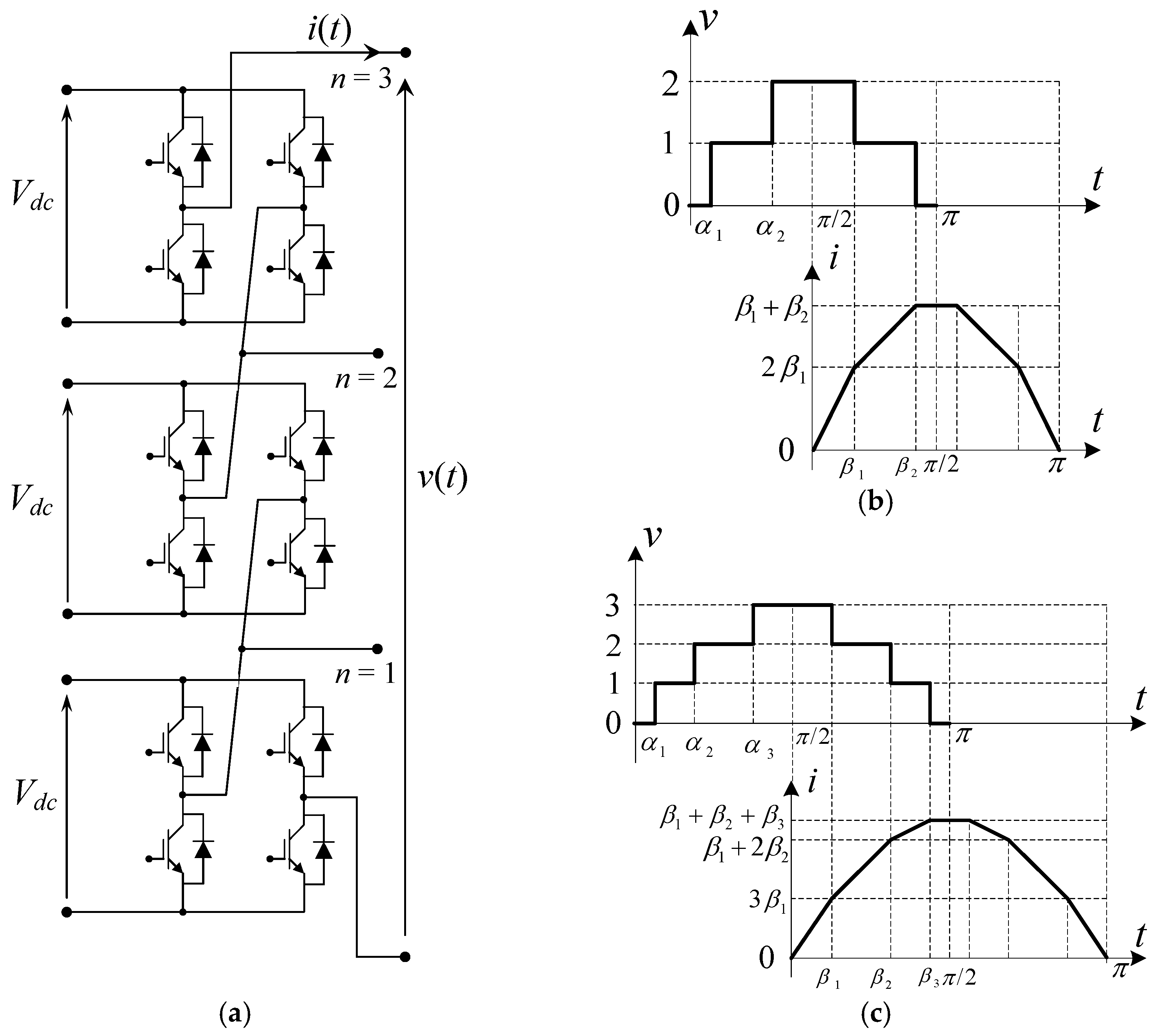
Figure 1 gives an example of cascaded H-bridge single-phase inverter with
n = 1, 2, and 3 cells, and the output voltage waveforms (half-waves) in the case of staircase modulation with five and seven output voltage levels. Due to quarter-wave symmetry, there are two and three independent switching angles, respectively. Current waveforms (half-waves) are obtained by time integration of the voltage waveforms that assumes pure inductive (or inductively dominant) load.
A precise closed-form expression for voltage (current) approximation error normalized mean square (voltage ripple
NMS [
5]) may be obtained by integrating the squared (normalized) voltage waveform average following a quarter-wave symmetry, as Equation (1):
For a two-cell inverter (
n = 2) with five-level voltage waveform (
Figure 1b), the modulation index
m, using the direct Fourier series fundamental term calculation, is Equation (2):
The expression for the voltage approximation mean square error to be minimized becomes Equation (3):
Additionally, the switching angles limitations are Equation (4):
For a three-cell inverter (
n = 3) with seven-level voltage waveform (
Figure 1c), the modulation index
m and mean square error are Equations (5) and (6):
In this case, switching angle limitations are similar to Equation (4).
For an arbitrary cell count
n (
n switching angles and 2
n + 1 voltage levels), modulation index becomes Equation (7):
and voltage ripple
NMS is Equation (8):
Using the frequency domain definition, voltage
THD expression is determined using Equation (9):
The relationship between voltage ripple
NMS and voltage
THD, due to Parseval’s theorem (Rayleigh energy theorem), can be written as Equation (10):
For a given modulation index m, the voltage THD optimization problem is formulated as a constrained optimization one with THD in Equation (10) (NMS in Equation (8)) as a target function to be minimized, modulation index in Equation (7) as an equality constraint, and staircase modulation-imposed limitations on switching angles similar to Equation (4) as inequality constraints.
The challenge of a time-domain current
THD analysis in pure inductive load approximation (voltage
WTHD), as Equation (11):
is finding closed-form expressions for current approximation mean square error for piecewise linear (normalized) current waveforms obtained by time integration of their respective voltage waveforms (
Figure 1b,c).
For
Figure 1, the normalized current analysis for the pure inductive load, which assumes both normalized fundamental angular frequency and load inductance equal unity, fundamental current harmonic magnitude equals voltage modulation index
m.
Then, current ripple NMS may be calculated, similar to Equation (1), by calculating the (normalized) squared current waveform average on a quarter-wave interval.
For two and three angles, by direct current mean square value computation, current ripple
NMS is found using Equation (12):
For an arbitrary cell count
n (
n = switching angles, and 2
n + 1 = voltage levels), the general current
NMS formula becomes Equation (14):
To derive NMS in Equations (12)–(14), Matlab symbolic calculations were used because manual computations become too burdensome starting from three cells (three angles).
3. Optimal Voltage and Current Total Harmonic Distortion Solutions
The constrained
THD (
NMS) minimization problems with modulation index equality and switching angles inequality constraints described in the previous section are effectively solved by means of Matlab function
fmincon. Voltage and current optimization solutions for a single-phase five-cell multilevel inverter (up to 5 angles and 11 voltage levels) are shown in
Figure 2,
Figure 3,
Figure 4 and
Figure 5.
Over the interlevel modulation index intervals 1–2, 2–3, 3–4, 4–5, voltage and current quadratic approximation error (
NMS/
THD) local minima and maxima appear. Global voltage
THD minima found in [
15,
16] for up to 6–7 angles without explicitly indicating the modulation indices are, in fact, local minima of voltage
THD curve in
Figure 2.
Voltage and current optimal switching angles might be considerably different (
Figure 4 and
Figure 5), and current angles’ curves are much smoother. Over each interlevel interval, there are two working points at which voltage
THD optimal angles and current
THD (voltage
WTHD) optimal angles are identical, having the same modulation index. Regarding the aforesaid, for the selected modulation indexes the voltage and current
THDs are minimal.
Sensitivity study shows that optimal current
THD is much more susceptible to switching angles variations compared with optimal voltage
THD. The low susceptibility to angles variations of optimal voltage
THD is known from the previous research [
12,
13]. On the whole, a coarse piecewise constant optimal approximation is very robust from possible disturbances point of view, such as angle/level variations and rounding errors.
Comparing the optimal voltage and current THDs, the current THD is much more susceptible to switching-angles variations. This happens due to the fact that a supposed fine piecewise linear optimal approximation (compared to a coarse piecewise constant one) is more susceptible in terms of possibly being affected by some disturbances.
Making a comparison between optimal voltage and current
THD (
Figure 2 and
Figure 3), it might be seen that current
THD curve ripple is much larger considering the noticeable difference between adjacent maxima and minima in the order of 100%. This leads to the fact that current
THD may be essentially reduced just by selecting a proper converter working point (modulation index) selection. On the contrary, there might be a significant current
THD increase as a penalty for a detuned operation.
Regarding
Figure 2 and
Figure 3, note that the curve of
THD average trend can be approximated by simple hyperbolic approximations [
17].
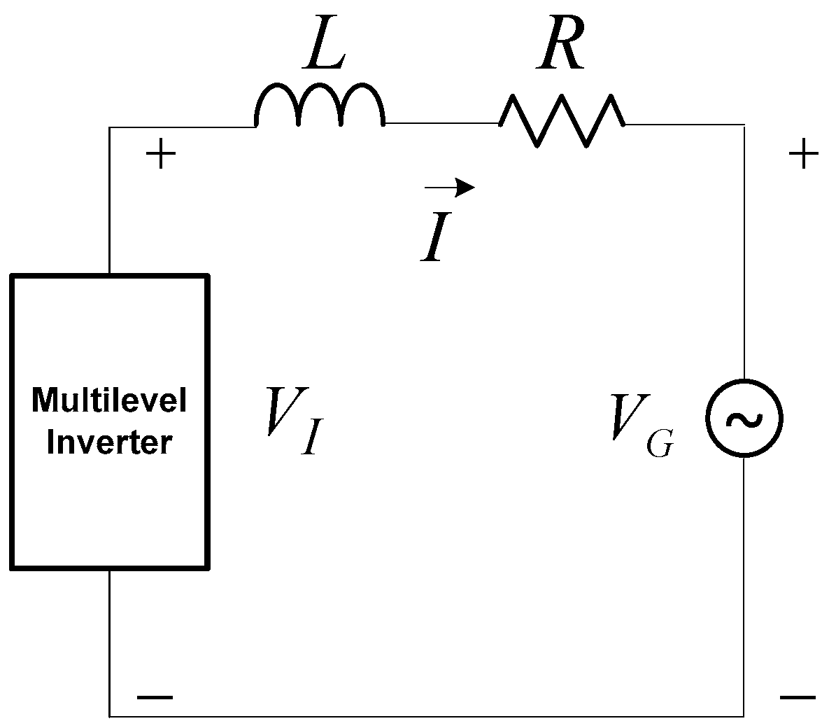
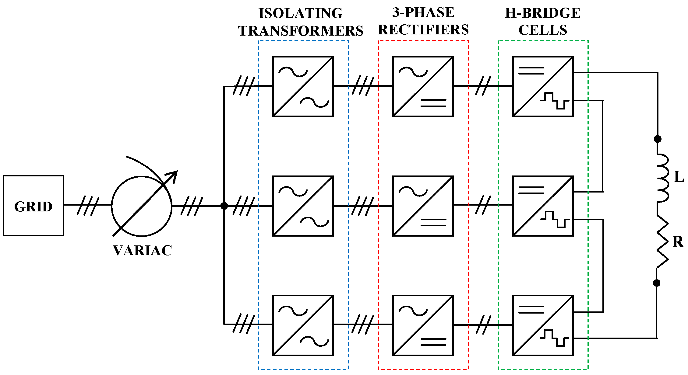
5. Laboratory Verification
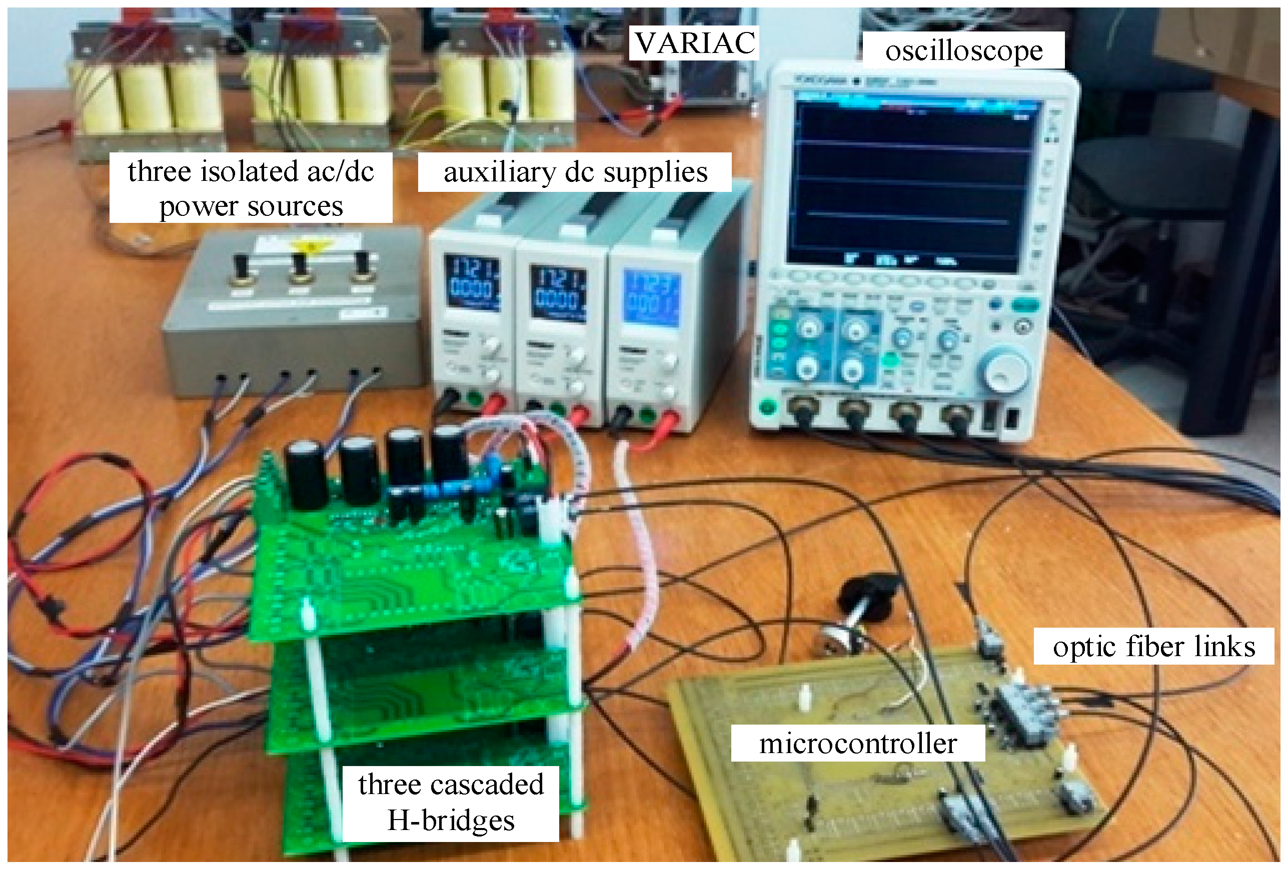
Experimental verifications were performed for a single-phase cascaded H-bridge inverter having three properly connected H-bridge cells (
n = 3), each one with the individual dc bus voltage
Vdc = 200 V, according to
Figure 1a,c. The circuit scheme of the experimental setup and the workbench are shown in
Figure 8 and
Figure 9.
It consists of three 3x Mitsubishi power IGBT modules IPM PS22A76 (1200 V, 25 A, Mitsubishi Electric Corporation, Tokyo, Japan), controlled by “Arduino Due” microcontroller board (84 MHz Atmel, SAM3X83 Cortex-M3 CPU, Somerville, MA, USA). The signal measuring equipment includes the PICO TA057 differential voltage probe (25 MHz, ±1400 V, ±2%, Pico Technology, Tyler, TX, USA) and LEM PR30 current probe (dc to 20 kHz, ±20 A, ±1%, LEM Europe GmbH, Fribourg, Switzerland) connected to the Yokogawa DLM 2024 oscilloscope (Yokogawa Electric Corporation, Tokyo, Japan). The LCR meter Agilent 4263B (Santa Rosa, CA, USA) was used to obtain the passive RL-load parameters, L = 481 mH, R = 24.7 Ω, measured at 100 Hz.
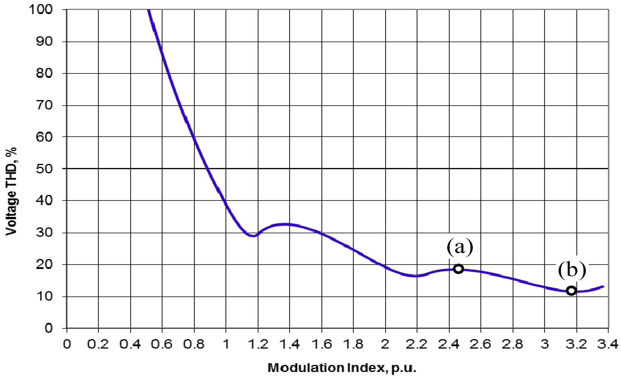
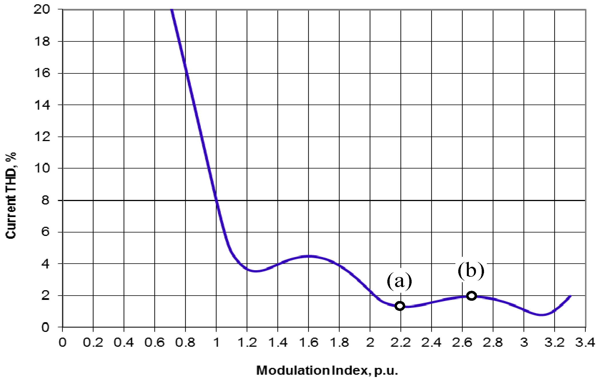
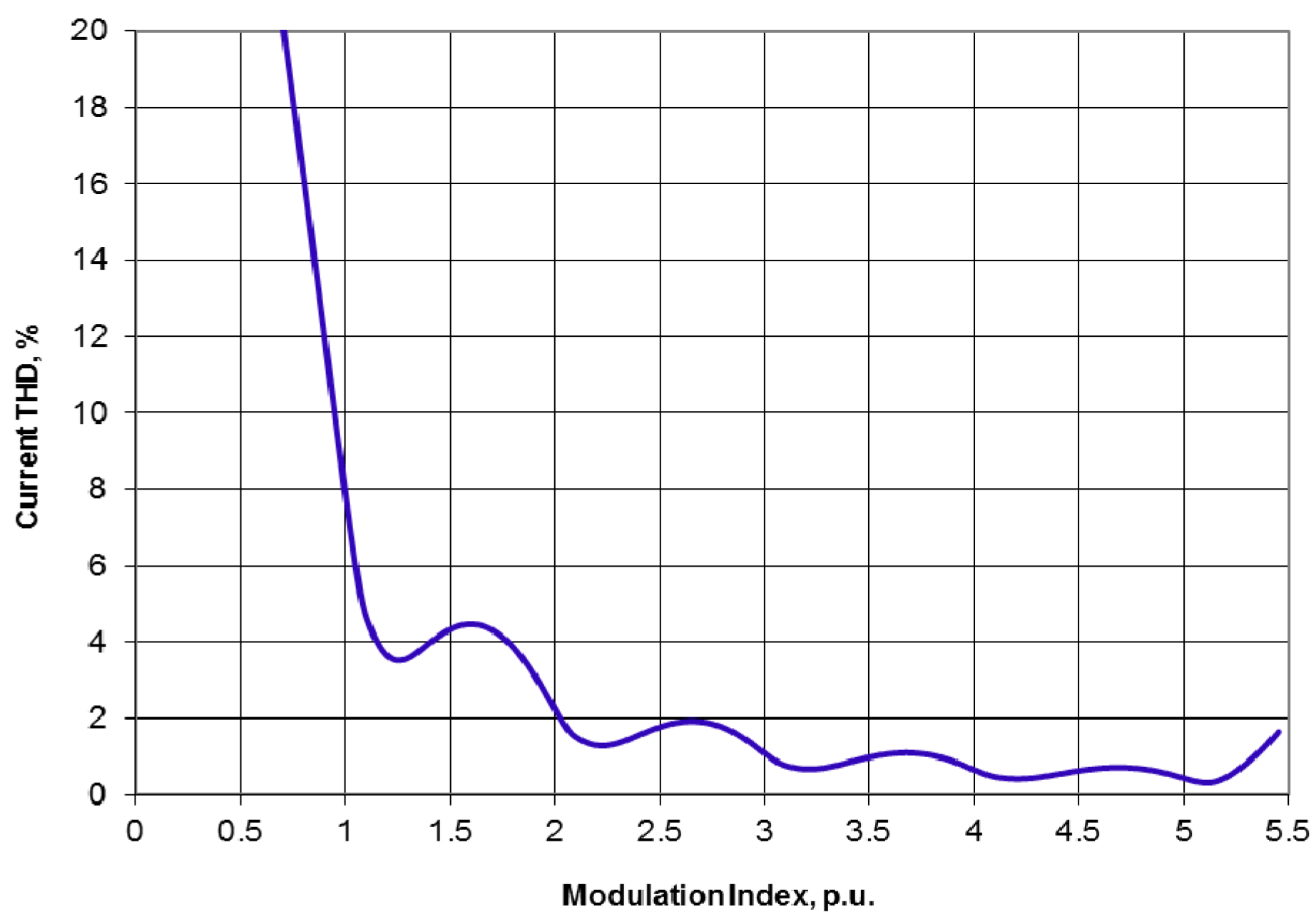
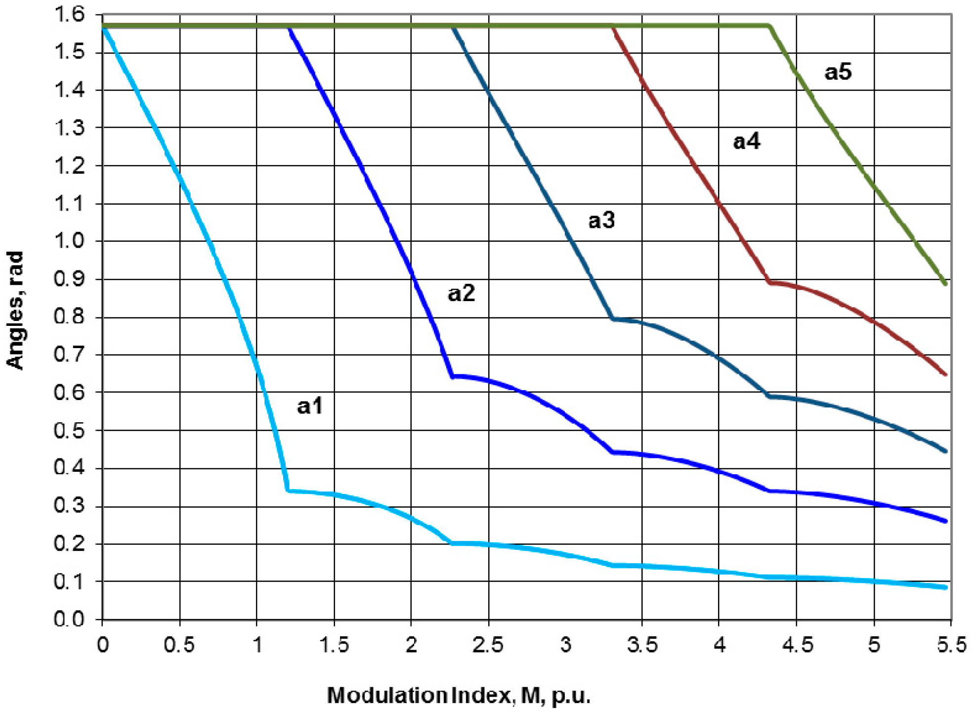
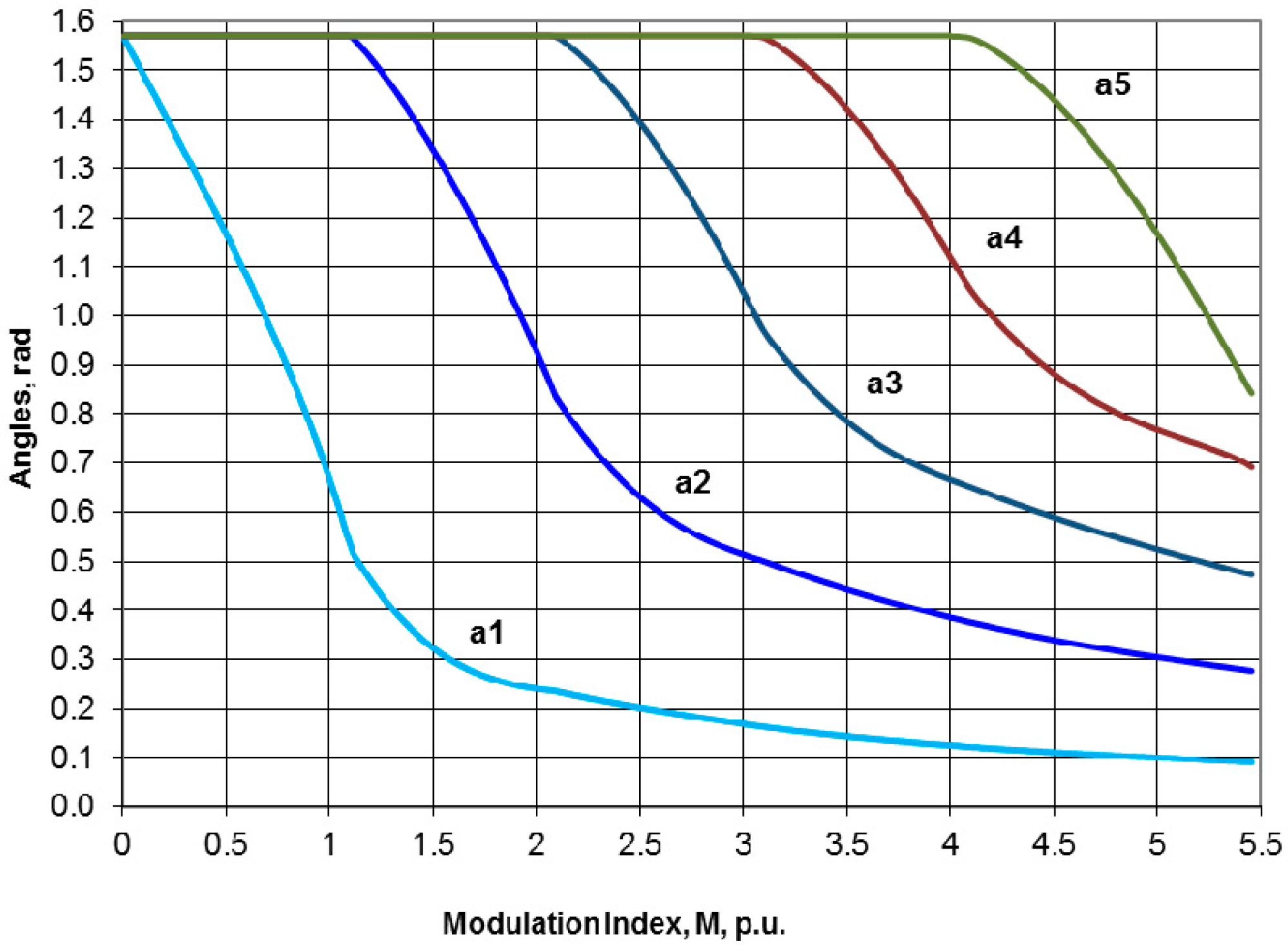
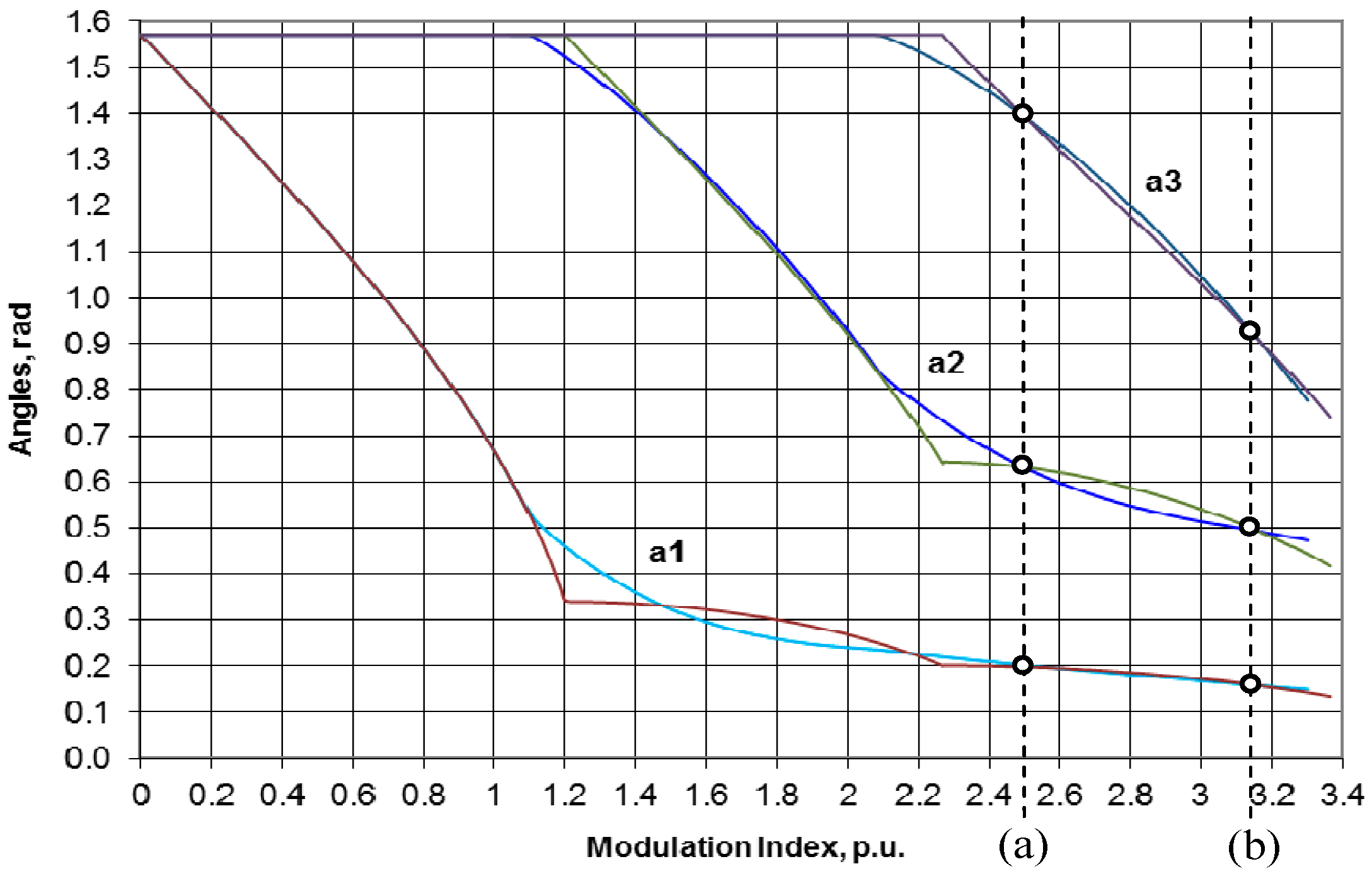
Minimal voltage and current
THD curves within the modulation index range for such inverter configuration (
n = 3, up to 7 voltage levels) are shown in
Figure 10 and
Figure 11. Voltage and current optimal switching angles are given in
Figure 12 (current angle curves are the smoother ones). Considering these figures, the six working conditions indicated by dots were chosen for the experimental tests. In particular, two test points (a) and (b) have been selected for minimum and maximum values of voltage and current
THDs over the modulation index range corresponding to seven levels, respectively (
Figure 10 and
Figure 11). Furthermore, two test points (a) and (b) have been selected corresponding to the modulation index
m when both voltage and current have the optimal values of
THD for the same three switching angles (
Figure 12).
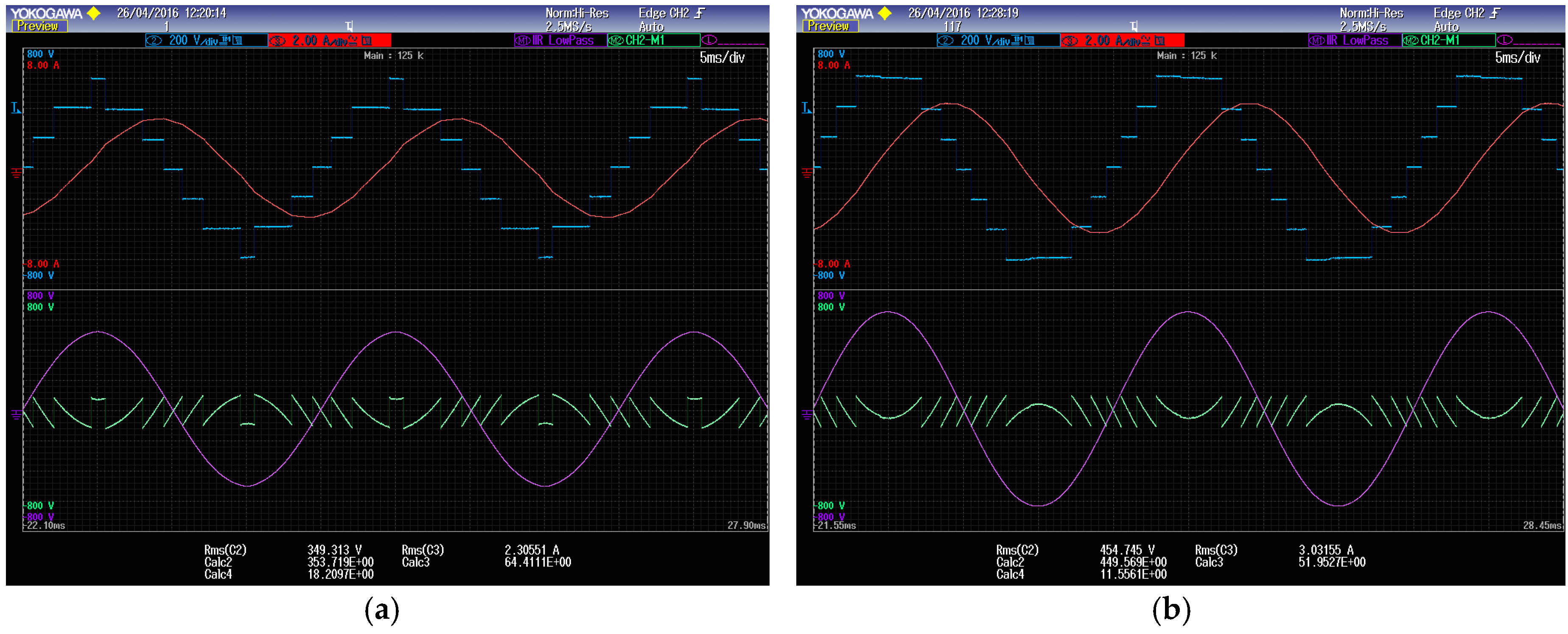
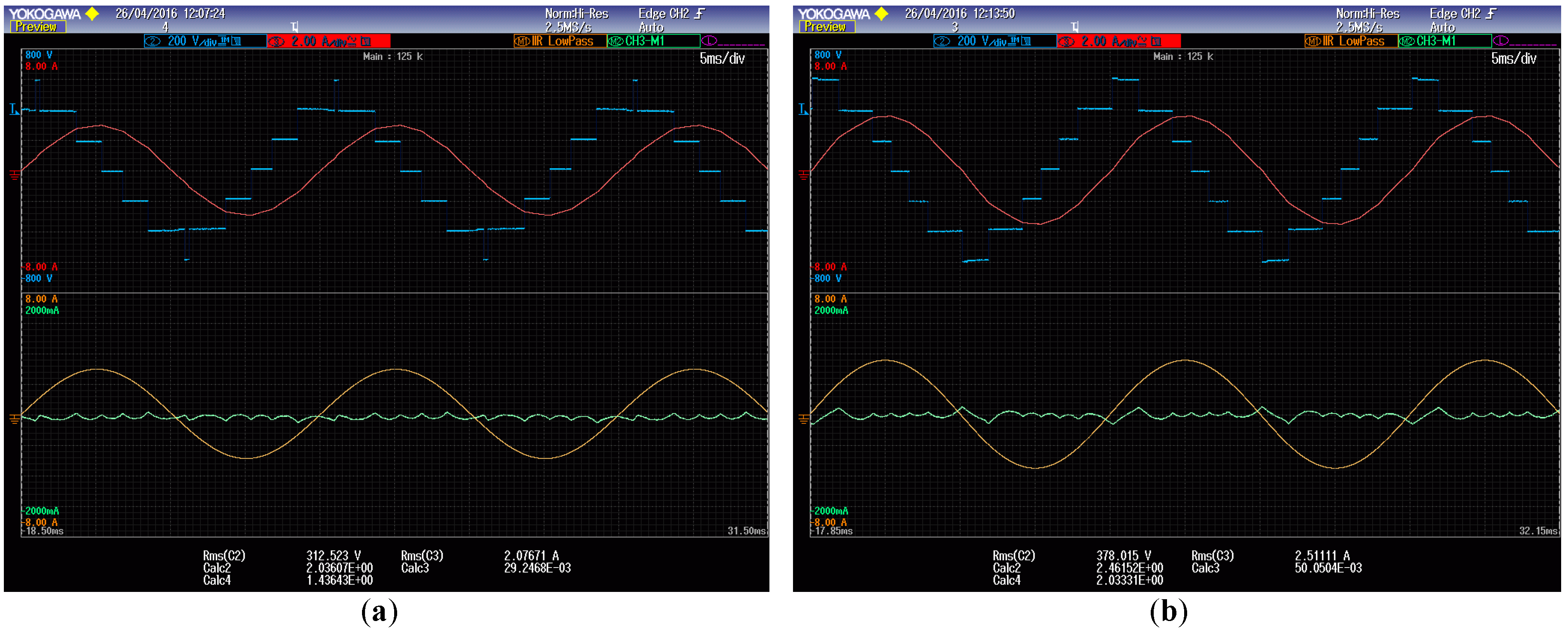
In
Figure 13,
Figure 14 and
Figure 15, the corresponding experimental results are presented, showing the test points (a) and (b). All figures depict the waveforms over the 2.5 fundamental periods. Due to limited scope functions, it is not possible to directly display full legends on screenshots. What can be noticed is that on the top of each screenshot the scales of waveforms are displayed with the colors which correspond to the waveform colors. Also, on the left side of all screenshots there are full-range scales with the same colors. The description of those waveforms is given in the first half of
Table 1: load voltage (blue trace)—scope channel 2, labeled C2 (CH2), load current (red trace)—scope channel 3, labeled C3 (CH3), the top half screen; fundamental of load voltage (purple trace), labeled M1, and voltage ripple (green trace), labeled M2: CH2 − M1, are depicted in the bottom half screen of
Figure 13 and
Figure 15; fundamental of load current (orange trace), labeled M1 and current ripple (green trace, magnified by 4), labeled M2: CH3 − M1, are depicted in the bottom half screen of
Figure 14 and
Figure 15. It should be noted that while calculating the voltage
THD, mathematical functions M1 and M2 are applied the load voltage waveform, and while calculating the current
THD they are applied to the load current waveform.
Fundamental components have been determined by built-in scope infinite impulse response (IIR) filter function (M1), and ripple components have been calculated as the difference between the actual waveforms and the corresponding fundamental components (M2 = CH2(3) − M1).
THDs have been determined as the ratio between ripple root mean square (
RMS) and fundamental
RMS. Specific calculation of
RMS and
THD for all voltage and current waveforms have been carried out by the scope built-in advanced mathematical functions in real time and displayed on the bottom lines of the scope screen. Corresponding designations with the calculation of voltage (current)
THD are presented in the last part of
Table 1.
Figure 13 presents two cases for local maximum and minimum values of the voltage
THD over the considered modulation index range.
Figure 13a corresponds to the case of local max
VTHD for
m = 2.459 (α
1 = 0.119, α
2 = 0.635, α
3 = 1.424), while
Figure 13b corresponds to the case of local min
VTHD for
m = 3.194 (α
1 = 0.155, α
2 = 0.482, α
3 = 0.884).
Figure 14 presents two cases for local minimum and maximum values of the current
THD over the considered modulation index range.
Figure 14a corresponds to the case of local min
ITHD for
m = 2.221 (α
1 = 0.224, α
2 = 0.758, α
3 = 1.527), while
Figure 14b corresponds to the case of local max
ITHD for
m = 2.663 (α
1 = 0.190, α
2 = 0.580, α
3 = 1.294).
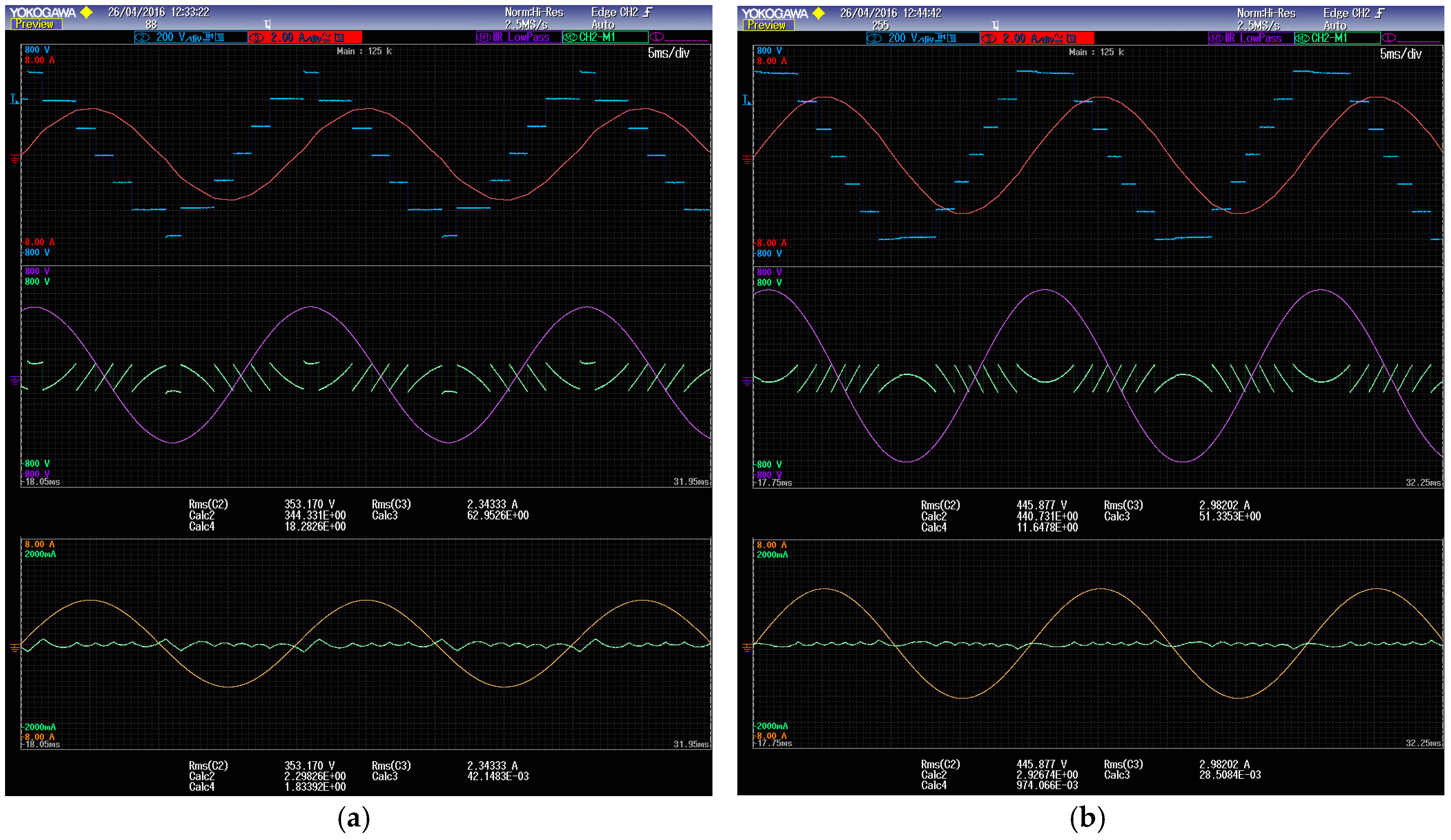
Figure 15 considers the cases of two modulation indices where optimal voltage
THD and optimal current
THD occur for the same switching angles, over the considered modulation index range.
Figure 15a corresponds to the case
m = 2.494 (α
1 = 0.202, α
2 = 0.633, α
3 = 1.397), while
Figure 15b corresponds to the case
m = 3.144 (α
1 = 0.160, α
2 = 0.495, α
3 = 0.925).
The experimental results (
Exp.) are summarized in
Table 2 and
Table 3, and compared with both theoretical calculations (
Calc.) and simulation results (
Sim., obtained by Matlab–Simulink).
Table 2 presents the four cases corresponding to
Figure 13a,b and
Figure 14a,b. It can be noticed that calculated, simulated, and experimental
THD% values have a really good matching in the case of minimized voltage
THD (left table side). In the case of current
THD (right table side), calculated values match the simulation ones, and the experimental values are slightly higher due to the really small values of the current ripple, which emphasize the measuring errors such as current probe errors and inverter nonlinearities (switching losses, dead-times, etc). Corresponding slight errors have been observed introducing similar nonidealities in the simulation tests.
Table 3 presents two cases (a) and (b) of
Figure 15, where the same three switching angles result for optimizing both the voltage and the current
THDs, corresponding to the same modulation index, as shown in
Figure 12. As expected, the experimental voltage
THD results match almost perfectly both theoretical and simulated results, while the current
THD results have slightly higher values, due to similar aforementioned reasons.
In general, the very slight difference between (ideal) simulations and calculated theoretical results in case of current THD can be justified, considering that the considered load is not pure inductive. In the specific test cases, the load impedance angle is about 81°, a bit lower than the theoretical angle of 90°. This is introducing a more than acceptably small error due to the high current THD sensitivity, proving the effectiveness of the assumption of inductively dominant load. On the whole, simulation and experimental results match the supposed ones in a satisfactory way.
6. Conclusions
Minimal voltage and current THD for a single-phase multilevel inverter with uniformly distributed voltage levels are formulated as constrained optimization ones in a time domain, considering all switching harmonics. Current THD is considered in a pure inductive load approximation (corresponding to voltage frequency weighted THD, WTHD). Comparing with minimal voltage THD time-domain problem formulations which have been reported previously, the minimal current THD time-domain problem formulation is a novel one. It becomes feasible due to analytical closed-form symbolic calculations of piecewise linear current waveform mean squares.
The numerical solutions establish theoretical calculation of voltage and current THD lower bounds for a single-phase multilevel inverter with a staircase modulation. Optimal switching angles and minimal voltage and current THDs are reported for different multilevel inverter cell numbers (different voltage level counts) and overall modulation index dynamic range. All calculations for optimal switching angles are quite simple and require a negligible processor time due to the fact that they can be easily calculated offline and called from the microcontroller memory. Also, every microcontroller can perform a simple linear interpolation, so high accuracy of the modulation index is not needed and, therefore, neither is its real-time calculation.
Over every interlevel modulation index interval, there are two working points which present the set of switching angles where the optimal voltage and current THD are achieved. Modulation indexes which correspond to those two working points are so-called twice optimal modulation indices.
It is shown that optimal voltage THD solutions have relatively low sensitivity to switching angles variations and other disturbances. On the other hand, sensitivity of current optimal solutions is relatively high due to a fine piecewise linear optimal approximation which is much more susceptible to possible disturbances compared with a coarse piecewise constant optimal one.
In the case of grid-connected applications, normalized current fundamental harmonic is typically about 10 times smaller than the voltage modulation index. Following this, the THD value of the grid-connected current increases in the same proportion, due to the direct proportion between the current THD and the normalized current magnitude, compared with the case when there is an inductively dominant load. This comparison is valid for the same modulation indexes for both practical cases. It is shown that only about 10% modulation index variations might cause around 100% of current THD changes. Considering this, there is a space for examining the optimal working point from the point of view of the minimal current THD values, and controlling in parallel the dc bus and grid voltage variations.
Theoretical findings are solidified by computer simulations and a wide set of laboratory verification. Experimental results confirm the correctness of the proposed mathematical approach for pure inductively dominant load for voltage and current THD calculations.


